Fabrication and optoelectronic properties of core–shell biomimetic ZnO/Si nanoball arrays
Yuan-Ming
Chang
*a,
Pin-Hsu
Kao
b,
Mao-Chen
Liu
c,
Chih-Ming
Lin
d,
Hsin-Yi
Lee
ef and
Jenh-Yih
Juang
*a
aDepartment of Electrophysics, National Chiao Tung University, Hsinchu 300, Taiwan. E-mail: ymchang7@gmail.com; jyjuang@g2.nctu.edu.tw; Fax: +886-3-5725230; Tel: +886-3-5712121 ext. 56116.
bCenter for Measurement Standards, Industrial Technology Research Institute, Hsinchu 300, Taiwan
cNational Nano Device Laboratory, Tainan 741, Taiwan
dDepartment of Applied Science, National Hsinchu University of Education, Hsinchu 300, Taiwan
eProgram for Science and Technology of Accelerator Light Source, National Chiao Tung University, Hsinchu 300, Taiwan
fDepartment of Materials Science and Engineering, National Chiao Tung University, Hsinchu 300, Taiwan
First published on 19th September 2012
Abstract
We report an effective process scheme comprising a single-step Ag sputtering with subsequent dry etching and atomic layer deposition (ALD) process for fabricating biomimetic ZnO/Si nanoball (ZnO/Si-NB) core–shell nanostructures directly on Si substrates. The obtained ZnO/Si-NB core–shell nanostructures consist of ∼30 nm thick ZnO films grown on Si frustums produced by means of dry etching masked by the self-assembled silver nanodots created by single-step sputtering. The ZnO films were deposited using atomic layer deposition under an ambient temperature of 200 °C. The photoluminescence (PL) measurements on these ZnO/Si-NB core–shell nanostructures showed that the visible range emission was almost completely absent and only the ultraviolet emission (3.28 eV peak) resulting from the free excitons was observed, indicating that the films indeed have high crystalline quality. Moreover, a dramatic improvement of the field emission performance was observed for ZnO/Si-NB core–shell nanostructures as compared to the bare Si frustum arrays. The detailed analyses on the field enhancement factor (β value) based on the Fowler–Nordheim field emission model indicate that the effective work function of the ZnO/Si-NB core–shell nanostructures might be significantly different from that of either ZnO or Si.
1. Introduction
Semiconductor nanomaterials have been attracting substantial experimental interest in recent years, in part due to their practical importance in manufacturing high-performance optoelectronic micro/nano devices.1–3 Among the wide array of nanomaterials being explored, ZnO has received exceptionally extensive attention owing to its unique physical characteristics, such as wide bandgap (∼3.37 eV) and large exciton binding energy (∼60 meV), as well as chemical robustness and thermal stabilities. In addition to the fundamental scientific interest, these competitive advantages further make various ZnO-derived nanostructures promising candidates in a wide spectrum of practical applications. In particular, it has been pointed out recently that ZnO is also a bio-safe, bio-compatible material.4 Thus, investigations toward developments of biomimetic nanostructures to serve as novel platforms and templates for creating new material forms have become topics of extensive interest. In this regard, a more comprehensive investigation in establishing simple and reliable fabrication processes, as well as understanding the optoelectronic features unique to the obtained biomimetic nanostructures is crucial. To date, direct fabrication of complex ZnO nanostructures with controlled morphologies remains challenging. Over the last decade or so, vapor-phase transport process carried out in a furnace5,6 and hydrothermal solution synthesis7 have been among the most popular methods utilized to produce oriented ZnO nanostructures. However, the above-mentioned methods either require high growth temperature or are time consuming. Thus, developing alternatives capable of lowering the process temperature, shortening the process time and, in particular, incorporating with existing Si technologies, for producing desired ZnO nanostructures is highly demanded.In this paper, we report an effective fabrication scheme for obtaining core–shell frog-egg-like biomimetic ZnO/Si-nanoballs (ZnO/Si-NBs) on a Si substrate. The biomimetic nanostructure comprises a layer of polycrystalline ZnO film grown on well-aligned Si-frustums, which were created by a self-assembled silver nanomask and subsequent dry etching process. After the formation of the aligned Si-frustums, a layer of ZnO film was then deposited by atomic layer deposition (ALD) at a growth temperature of 200 °C to form the core–shell Si-NBs array. To the best of our knowledge, both the low growth temperature (∼200 °C) and tremendous time-saving accomplished have made the present fabrication method by far the most effective one in obtaining ZnO/Si-NB core–shell nanostructures. Furthermore, the optoelectronic properties manifested in these ZnO/Si-NB core–shell nanostructures exhibit not only highly effective intrinsic ultraviolet (UV) emission in photoluminescence (PL) measurements, but also very competitive field emission characteristics, which is attributed primarily to electronic band structure modifications originating from the sharp interface between the ZnO layer and underneath Si frustums.
2. Experimental
The Ag-nanodots dispersed on the Si substrate were obtained by rf-sputtering from an Ag target (Eastern Sharp EPS01) for 5 s with an input power of 150 W and 25 sccm argon gas at room temperature. The Ag nanodots then served as natural metal-nanomasks for subsequent dry etching performed on the Ag-coated Si substrate to create well-aligned Si frustum arrays. Prior to etching, the chamber was evacuated to a base pressure of 3 × 10⁻⁵ Torr and the system temperature was kept at 60 °C. After the Ag-coated Si substrate was loaded, flowing gas consisting of 90 sccm Cl2 and 10 sccm N2 was introduced into the chamber. The system was operated at a fixed input power of 3000 W with an etching time of 1 min.A layer of ZnO film was then deposited by ALD on the etched Si substrate at 200 °C. The ALD process is essentially a film growth technique comprising a series of self-limiting vapor-phase chemisorptions, the efficiency of which depends primarily on consecutive surface reactions. In practice, critical purge steps are applied to prevent the reactive precursors from interacting with each other. In this study, the pulse durations of water and diethylzinc (DEZn) were fixed at 100 ms and 50 ms, respectively. The purge and pumping periods were both kept at 15 s and N2 was used as the purge gas with the pressure being set at 3 × 10⁻³ Torr. With this practice scheme, the films are expected to grow in a monolayer-by-monolayer fashion. Moreover, it has been demonstrated previously that the ZnO films with very smooth surface could be obtained by incorporating the ALD process with an interrupted flow.8 In this work, a similar technique was adopted to deposit ZnO films on the surface of the etched Si substrates. With 150 ALD cycles the thickness of the obtained ZnO films was estimated to be about 30 nm.
The characteristics of surface morphology and film cross-section was examined by using a field-emission SEM (JEOL JSM-6700F), and the compositions of the films were analyzed by EDS. The structural characteristics of the ZnO/Si-NBs were investigated by a high-resolution X-ray diffractometer operated at 45 kV and 40 mA using Cu-Kα radiation (λ = 1.54 Å) with grazing angle scan. AFM was used to reveal the surface morphology of the ZnO/Si-NBs in more detail. Cross-sectional TEM (JEOL JEM-2010F) with an operating voltage of 200 kV was used to examine the microstructures of the ZnO/Si-NBs, especially the details of individual ZnO/Si-NB core–shell nanostructures. PL was measured at room temperature using a He–Cd laser (325 nm) for excitation and a CCD with a monochromator for detection to delineate the crystalline quality of the ALD-derived ZnO layer. For field emission measurements, the samples were loaded into a vacuum chamber (2 × 10⁻⁶ torr). A transparent conductive oxide (indium-tin-oxide) coated with a layer of phosphor (P22) served as the anode electrode of the vacuum system and the field emission current was measured as a function of the cathode voltage applied to the ZnO/Si-NBs samples (1 × 1 cm2).
3. Results and discussion
As shown in Fig. 1a, the Ag nanodots obtained by extremely short time (∼5 s) rf-sputtering has a rather uneven size distribution, ranging from 5–30 nm in diameter, over the entire Si substrate. It is noted that these self-assembled Ag nanodots are generated as a direct consequence of single-step rf-sputtering and no further heat treatment was introduced. Since the Ag nanodots are rather isolated from each other with a wide range of size distribution, it is indicative that the Ag layer may have followed the Volmer–Weber growth mode.9–11 Moreover, as will be shown below, these Ag-nanodots serve very well as natural nanoscale metal-masks for subsequent anisotropic etching to be performed on Si substrates. Indeed, as shown in Fig. 1b, oriented Si-nanostructures are obtained on the Si substrate partially covered with the Ag-nanodots shown in Fig. 1a after 1 min dry etching. The nano-sized Si frustums obtained under these conditions have an average aspect ratio of ∼1–1.5 and there is no residual masking Ag-nanodot on top of the nano-sized Si frustums. The obtained nano-sized Si frustums appear to be preferentially vertically oriented, indicating the effectiveness of Ag nanomasks for anisotropic etching. Thus, from a practical point of view, the simplicity of the present fabrication method can be advantageous in several aspects. First, the fabrication process is very effective because it took only 5 s to obtain the self-assembled Ag-nanomask by sputtering. Second, the lithography-free anisotropic dry etching can further reduce the fabrication cost significantly.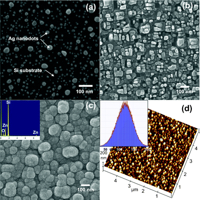 | ||
| Fig. 1 The SEM images of (a) Ag nanodots array; (b) the Si-substrate covered with Ag nanodots after being dry ecthed for 1 min; (c) the biomimetic surface with ZnO/Si-NBs core–shell nanostructures. (d) is the three-dimensional AFM image of (c), and the inset in (d) is the height distribution of ZnO/Si-NBs. | ||
In order to utilize the obtained nano-sized Si frustums to fabricate the biomimetic core–shell semiconductor heterostructures, ALD was chosen because of its capability to form an extremely thin layer conformable to surfaces with complex morphologies. As mentioned above, ALD comprises a series of self-limiting vapor-phase chemisorption processes with intermittent critical purge steps to prevent reactive precursors from interacting with each other. The exact control of layer-by-layer growth inherently gives rise to excellent substrate morphology conformability and step-coverage, even when the ALD-derived films are only a few nanometers thick. As shown in Fig. 1c, the morphology of the obtained film has a unique frog-egg-like biomimetic appearance with an average diameter of ∼100 nm. The inset of Fig. 1c shows the results of energy-dispersive X-ray spectroscopy (EDS) analysis on these biomimetic ZnO/Si-NBs, which clearly demonstrates the existence of both ZnO and Si, thus confirmsing the core–shell characteristics of the present ZnO/Si-NBs. Fig. 1d illustrates the typical three-dimensional (5 × 5 μm2) atomic force microscopy (AFM) image of the ZnO/Si-NBs, indicating that indeed the ZnO/Si-NBs resemble biomimetic frog eggs even more. Moreover, the inset in Fig. 1d reveals the height distribution of the ZnO/Si-NBs extracted from three-dimensional AFM measurements, which ranges mainly around 100–150 nm and gives rise to an aspect ratio of 1–1.5.
In order to further examine the crystalline structure of the ZnO films obtained by the current ALD process, grazing incidence X-ray diffractometry (XRD) was carried out. Fig. 2 shows the XRD spectra obtained for the ZnO/Si-NBs grown at 200 °C. It is evident that, with the grazing incidence experiment, the diffraction from the underneath Si substrate does not show up and there are only six distinctive diffraction peaks corresponding to (002), (101), (102), (110), (103) and (112) crystallographic orientations of the ZnO films observed. Moreover, the full-width at half-maximum (FWHM) of the (002) diffraction peak of ZnO/Si-NBs shown in the inset of Fig. 2 is ∼0.36°. The results suggest that although the ZnO layer remains largely polycrystalline, its crystalline quality is excellent. This is further confirmed by the more detailed structural information obtained from transmission electron microscopy (XTEM) examinations. Fig. 3a displays the TEM image of a typical section of the ZnO/Si-NBs. It is evident that the deposition of the ZnO layer does result in dramatic changes on the morphological features of the original Si frustums (Fig. 1b). The inset in Fig. 3a displays the electron diffraction pattern taken along the [110] zone-axis of Si. It is noted that, in addition to brighter ordered diffraction spots originating from single crystalline Si frustums, there are many randomly distributed diffraction spots with much weaker intensities in the diffraction pattern. Those presumably originate from the polycrystalline ZnO layer. The HRTEM image displayed in Fig. 3b clearly shows that every individual ZnO/Si-NB is composed of a layer of polycrystalline ZnO conformably covering the nano-sized Si frustum. It is evident that the randomly oriented ZnO nano-crystals consisting of the 30-nm-thick ZnO layer appear to have very good crystalline quality. Moreover, the crystallinity of the Si frustum remains essentially intact up to the very top surface layer, although it has been subjected to etching processes and subsequent ALD at 200 °C. In particular, although there is an apparent feature in the vicinity of the interface region between the Si frustum and ZnO layer, the ∼1-nm-thick interface region, however, is unlikely to be the amorphous native Si-oxides frequently seen in similar structures obtained with other manufacturing methods. The interface between the Si frustum and ZnO layer appears to be atomically sharp, except for the lower-left corner where the interface is blurred and the resulting ZnO grain has relatively poor crystallinity. Thus, the present ZnO/Si core–shell structures may be largely regarded as a heterojunction of two semiconductors without insulating oxides inbetween. As will be described later, this may have significant effects on the optoelectronic properties of the present ZnO/Si-NBs.
 | ||
| Fig. 2 The XRD spectra of ZnO/Si-NBs. The inset is the FWHM of the ZnO (002) peak. | ||
![The (a) TEM and (b) HRTEM images of ZnO/Si-NBs. The inset in (a) shows the diffraction pattern of the ZnO/Si-NBs taken with [110] zone-axis.](/image/article/2012/RA/c2ra21817h/c2ra21817h-f3.gif) | ||
| Fig. 3 The (a) TEM and (b) HRTEM images of ZnO/Si-NBs. The inset in (a) shows the diffraction pattern of the ZnO/Si-NBs taken with [110] zone-axis. | ||
Due to its non-destructive and informative features, PL has been ubiquitously used to reveal the intimate correlations between the optical properties and crystalline characteristics in various ZnO nanostructures.10–16 With respect to this, in Fig. 4 we compare the room-temperature PL spectra of the ZnO films deposited on Si frustums and on polished Si substrates. It can be observed from the PL spectra that both of the ZnO/Si-NBs (red solid circles) and ZnO/Si (blue solid triangles) exhibit a strong UV emission peak positioning around 3.28 eV with a FWHM approximately equal to 133 meV (see the inset of Fig. 4). The relatively narrow FWHM is indicative of the high crystalline quality of the ZnO layer. The high crystallinity of the ZnO films obtained at a growth temperature of 200 °C apparently have eliminated most of the structural defects, which not only blocked the self-compensation processes thermodynamically, but also removed most of the nonradiative recombination channels.15 As a consequence, it is conceivable that the strong UV emission (3.28 eV peak) results primarily from the intrinsic near-band-edge (NBE) emission.17,18 Moreover, we also noted that the intensity of the 3.28 eV emission peak for the ZnO/Si-NBs is about 2 times larger than that obtained from ZnO/Si, although both were deposited under exactly the same conditions. This is attributed to the higher surface area offered by the Si frustums for growing ZnO/Si-NBs, which has allowed more ZnO material to be grown on the template and led to markedly more efficient free exciton emission.15,16 Finally, the PL spectra evidently displays a nearly complete suppression of emissions in the visible range, which has been identified to be intimately associated with the existence of massive defects, such as oxygen vacancies and Zn interstitials.10–16 This is, in fact, in very good agreement with the HRTEM results displayed in Fig. 3b, where the lattice image evidently exhibits excellent crystallinity of individual ZnO crystallites throughout the entire ZnO/Si-NB core–shell structure.
 | ||
| Fig. 4 The room temperature PL spectrum of ZnO/Si-NBs and ZnO films directly deposited on polished Si. The inset is the FWHM of the UV peak for ZnO/Si-NBs. | ||
To further explore how the ZnO/Si-NB core–shell structure may possibly modify the electronic properties of the original Si frustum structure, field emission measurements were performed on both structures. Fig. 5a shows the results of emission current density versus applied electrical field (J–E) curves obtained from both structures. Here, the electric field was calculated by dividing the applied voltage with the spacing between the cathode and the anode, thus this should be taken as an average value. Steady field emission was obtained by keeping the distance between the electrodes at 150 μm and the chamber pressure at 2 × 10⁻⁶ Torr during measurements.
 | ||
| Fig. 5 The field emission J–E curve from the Si frustums (blue triangles) and ZnO/Si-NBs (red circles) at a working distance of 150 μm over an effective emitting area of 1 cm2. The inset shows the corresponding F–N plot (ln (J/E2) vs. (1/E)) reveals the two-slope characteristic of ZnO/Si-NBs. (b) The emission current as a function of time operated at 5.1 V μm−1, showing the robustness of the ZnO/Si-NB nanostructures. | ||
It is evident from Fig. 5a that, for the pristine Si frustums, field emission current was hardly detected up the maximum applied field (∼5.3 V μm−1) of the current setup. This is presumably due to the existence of the native oxide layer, which forms an insurmountable barrier for electron emission. On the other hand, for the ZnO/Si-NB core–shell structures, the turn-on field (defined as the applied field to draw an emission current of 1 μA cm−2) is about 3.13 V μm−1. The observed turn-on field is not only lower than those reported for various pure ZnO nanostructures, such as nanorods,19 nanowires20 and nanoneedle arrays,21 but, even more importantly, demonstrates the drastic modification in the electronic properties of original Si frustums induced by merely depositing a shell layer of ZnO. Moreover, it is noted that the emission current density reaches ∼150 μA cm−2 at the maximum bias field of our current setup (∼5.3 V μm−1), which also outperforms most of the previously reported ZnO nanostructures, such as ZnO nanowire and microcalabashe,22 nanopillars23 and nanowalls arrays.24
In order to delineate the emission behavior in a more quantitative manner, the J-E results are analyzed by the Fowler–Nordheim (F–N) equation (eqn (1)):10,11
 | (1) |
| β = −(6.83 × 10³ × ϕ3/2)/slope | (2) |
The inset in Fig. 5a shows the F–N plot for the core–shell ZnO/Si-NBs, which evidently exhibits the two-slope behavior, suggesting that the field emission behavior of these ZnO/Si-NBs may have deviated from the F–N description. The two-slope behavior in the F–N plot has been observed in a wide variety of semiconductor nanostructures18,25,26 and even carbon nanotubes. It was explained on the basis of electron emission from the conduction band (CB) and valence band (VB) of the semiconductor.18 However, although ϕZnO = 5.3 eV has been the most cited value for ZnO,10,11 when emission from the bottom of the conduction band is considered, it should be taken as 3.8–4.2 eV27–29 and the valence band is about 3.37 eV below the conduction band. In such cases, according to eqn (2), a substantial slope change of 2–2.5 times is expected assuming β remains constant. Here, a slope change of about 3.2 times is observed. Since in the present case, the emission structure comprises two different semiconductors, thus the simple scenario of emission from CB and VB of the same semiconductor may not be applicable. Alternatively, the two-stage emission phenomenon was attributed to the space charge effect, localized state, adsorbate-enhanced tunneling states and/or variation of the local field.
Very recently, Kale et al.4 prepared a high aspect ratio ZnO/Si-nanowire (ZnO/Si-NW) core–shell array and indicated that, by considering the respective work function and electron affinity (the energy difference between the vacuum level and the bottom of the conduction band for Si and ZnO), the conduction band of ZnO should be about 0.45 eV below that of Si. As a result, electrons would transfer easily from Si to ZnO and the ZnO layer would act as an electron reservoir. Furthermore, their core–shell structure appeared to have substantial amount of defects, as revealed in the PL spectra. Thus, interfacial charge accumulation due to the Maxwell–Wagner effect30 may also play a role in the field emission properties exhibited in their ZnO/Si-NW arrays. In our case, since both the XTEM and PL analyses showed that the interface of the ZnO/Si-NBs and the ZnO layer are all of high crystalline qualities, thus the latter effect might not be as significant. A rough estimation on the corresponding β values for the present ZnO/Si-NBs can be made from the F–N plot by assuming ϕZnO ∼ 5.3 eV for ZnO and the obtained β values are 6242 and 1993 for low-field and high-field regimes, respectively. However, if we consider the accumulated electrons on the ZnO layer level and the conduction bottom of Si and take the electron affinity of Si (ϕSi ∼ 4.1 eV) as the effective work function of the ZnO/Si-NB core–shells, the obtained β values become 4247 and 1356 for low-field and high-field regimes, respectively. In either case, the obtained field enhancement factor values in high-field regime (where the emission current reaches the practical values) are larger than that of a ZnO nanoneedle array,31 nanotube array32 and nanowires,33 indicating that the aspect ratio (only about 1–1.5 in the present case) of the emitter might not be the most critical parameter for obtaining decent emission properties. This is of particular significance when the robustness of the emission structures is considered. To demonstrate the robustness of the current ZnO/Si-NB core–shells, Fig. 5b shows the emission current density as a function of time operated at 5.1 V μm−1. It is evident from the results that, although it appears to be fluctuating (presumably due to the simple circuitry of our measuring setup), the current density does not show any sign of diminishing over the 2 h period of continuous testing. Together with the low turn-on field described above, the current ZnO/Si-NB core–shells can be regarded as excellent field emitters and should be of great potential for various field emission-associated applications.
4. Conclusions
In summary, we have demonstrated an effective low-temperature process scheme comprising a single-step Ag sputtering with subsequent dry etching and ALD process for obtaining oriented ZnO/Si-NB core–shell biomimetic nanostructures. The ZnO/Si-NB core–shell structures obtained by the present simple and lithography-free process scheme not only have excellent crystalline quality over the entire structure, but also exhibit field emission performance superior to most of the ZnO nanostructures reported previously. The enhancement of the field emission properties is more relevant to the modification of effective work function in these core–shell semiconductor heterostructures, rather than interface charge accumulation induced by the Maxwell–Wagner effect or defect trapping. The robustness and effectiveness in field emission demonstrated by the current ZnO/Si-NB core–shell structures evidently indicate the tremendous potential of using them in various field-emission-derived applications.Acknowledgements
This work was partially supported by the National Science Council of Taiwan, under Grant No.: NSC 101-2811-M-009-044. Prof. J.-Y. Juang is supported in part by the National Science Council of Taiwan and the MOE-ATP program operated at NCTU. The authors would also like to thank Prof. Hsi-Fu Shih (NCHU), Prof. Ching-Liang Dai (NCHU) and Jyun-Hao Wu (NCHU) for sputtering, and Dr Yu-Hwa Shih, Dr Jheng-Ming Huang (NCTU), Dr Shang-Jui Chiu (NCHU), Dr Yen-Ting Liu (NCTU) and Che-Hsieh Chiu (NCTU) for useful discussion.References
- J. Guan, J. Zhang, T. Yu, G. Xue, X. Yu, Z. Tang, Y. Wei, J. Yang, Z. Li and Z. Zou, RSC Adv., 2012, 2, 7708 RSC.
- R. Li, Y. Luan, H. Zou, J. Du, T. Mu and Z. Li, RSC Adv., 2012, 2, 3049 RSC.
- K. K. Wong, A. Ng, X. Y. Chen, Y. H. Ng, Y. H. Leung, K. H. Ho, A. B. Djurisic, A. M. C. Ng, W. K. Chan, L. Yu and D. L. Phillips, ACS Appl. Mater. Interfaces, 2012, 4, 1254 CAS.
- V. S. Kale, R. R. Prabhakar, S. S. Pramana, M. Rao, C.-H. Sow, K. B. Jinesh and S. G. Mhaisalkar, Phys. Chem. Chem. Phys., 2012, 14, 4614 RSC.
- C. Li, G. Fang, J. Li, L. Ai, B. Dong and X. Zhao, J. Phys. Chem. C, 2008, 112, 990 CAS.
- Z. Zhang, S. J. Wang, T. Yu and T. Wu, J. Phys. Chem. C, 2007, 111, 17500 CAS.
- Y. Sun, N. A. Fox, D. J. Riley and M. N. R. Ashfold, J. Phys. Chem. C, 2008, 112, 9234 CAS.
- C.-S. Ku, J.-M. Huang, C.-M. Lin and H.-Y. Lee, Thin Solid Films, 2009, 518, 1373 CrossRef CAS.
- Y.-M. Chang, J. Shieh and J.-Y. Juang, J. Phys. Chem. C, 2011, 115, 8983 CAS.
- Y.-M. Chang, M.-C. Liu, P.-H. Kao, C.-M. Lin, H.-Y. Lee and J.-Y. Juang, ACS Appl. Mater. Interfaces, 2012, 4, 1411 CAS.
- Y.-M. Chang, J.-M. Huang, C.-M. Lin, H.-Y. Lee, S.-Y. Chen and J.-Y. Juang, J. Phys. Chem. C, 2012, 116, 8332 CAS.
- V. A. Fonoberov and A. A. Balandin, Phys. Rev. B, 2004, 70, 195410–1 CrossRef.
- V. A. Fonoberov and A. A. Balandin, Appl. Phys. Lett., 2007, 85, 5971 CrossRef.
- T.-Y. Chiang, C.-L. Dai and D.-M. Lian, J. Alloys Compd., 2011, 509, 5623 CrossRef CAS.
- Y.-M. Chang, J. Shieh, P.-Y. Chu, H.-Y. Lee, C.-M. Lin and J.-Y. Juang, ACS Appl. Mater. Interfaces, 2011, 3, 4415 CAS.
- Y.-M. Chang, S.-R. Jian, H.-Y. Lee, C.-M. Lin and J.-Y. Juang, Nanotechnology, 2010, 21, 385705–1 CrossRef.
- Y. Zhang, F. Lu, Z. Wang and L. Zhang, J. Phys. Chem. C, 2007, 111, 4519 CAS.
- T. Premkumar, Y. S. Zhou, Y. F. Lu and K. Baskar, ACS Appl. Mater. Interfaces, 2010, 2, 2863 CAS.
- R. T. R. Kumar, E. McGlynn, C. McLoughlin, S. Chakrabarti, R. CSmith, J. D. Carey, J. P. Mosnier and M. O. Henry, Nanotechnology, 2007, 18, 215704–1 CrossRef.
- X. Wang, J. Zhou, C. i. Lao, J. Song, N. Xu and Z. L. Wang, Adv. Mater., 2007, 19, 1627 CrossRef CAS.
- Y.-K. Tseng, C.-J. Huang, H.-M. Cheng, I.-N. Lin, K.-S. Liu and I.-C. Chen, Adv. Funct. Mater., 2003, 13, 811 CrossRef CAS.
- B. Cao, X. Teng, S. H. Heo, Y. Li, S. O. Cho, G. Li and W. Cai, J. Phys. Chem. C, 2007, 111, 2470 CAS.
- D. Pradhan, M. Kumar, Y. Ando and K. T. Leung, ACS Appl. Mater. Interfaces, 2009, 1, 789 CAS.
- D. Pradhan, M. Kumar, Y. Ando and K. T. Leung, Nanotechnology, 2008, 19, 035603–1 CrossRef CAS.
- C. X. Xu, X. W. Sun, S. N. Fang, X. H. Yang, M. B. Yu, G. P. Zhu and Y. P. Cui, Appl. Phys. Lett., 2006, 88, 161921–1 CrossRef.
- N. S. Ramgir, D. J. Late, A. B. Bhise, I. S. Mulla, M. A. More, D. S. Joag and V. K. Pillai, Nanotechnology, 2006, 17, 2730 CrossRef CAS.
- C. Ye, Y. Bando, X. Fang, G. Shen and D. Golberg, J. Phys. Chem. C, 2007, 111, 12673 CAS.
- X. Wang, X. Kong, Y. Yu and H. Zhang, J. Phys. Chem. C, 2007, 111, 3836 CAS.
- J. Im, J. Singh, J. W. Soares, D. M. Steeves and J. E. Whitten, J. Phys. Chem. C, 2011, 115, 10518 CAS.
- K. B. Jinesh, Y. Lamy, J. H. Klootwijk and W. F. A. Besling, Appl. Phys. Lett., 2009, 95, 122903–1 CrossRef.
- H. Y. Yang, S. P. Lau, S. F. Yu, L. Huang, M. Tanemura, J. Tanaka, T. Okita and H. H. Hng, Nanotechnology, 2005, 16, 1300 CrossRef CAS.
- X.-P. Shen, A.-H. Yuan, Y.-M. Hu, Y. Jiang, Z. Xu and Z. Hu, Nanotechnology, 2005, 16, 2039 CrossRef CAS.
- C. J. Lee, T. J. Lee, S. C. Lyu, Y. Zhang, H. Ruh and H. J. Lee, Appl. Phys. Lett., 2002, 81, 3648 CrossRef CAS.
| This journal is © The Royal Society of Chemistry 2012 |