
Charge transfer excitons in unfunctionalized graphite-wrapped MAPbBr3 nanocrystal composites with different morphologies†
Gaurav Kumar
Nim
a,
Sukanya
Ghosh
a,
Saurabh Kumar
Saini
b,
Mahesh
Kumar
 *b and
Prasenjit
Kar
*a
*b and
Prasenjit
Kar
*a
aDepartment of Chemistry, Indian Institute of Technology Roorkee, Roorkee, Uttarakhand 247667, India. E-mail: kar.prasen@gmail.com
bAdvanced Materials & Device Metrology division, National Physical Laboratory, New Delhi 110012, India. E-mail: Mkumar@nplindia.org
First published on 7th April 2022
Abstract
Highly luminescent methylammonium lead halide perovskite nanocrystals (PNCs) have attracted considerable research interest due to their alluring properties that can be tuned as per the morphological variations. Charge transfer excitons (CTEs) are a good representation of the capacity of semiconductor materials to tune their properties. We report here that CTEs may be generated successfully in graphite:PNC composites functioning as host–guest components. These hybrid perovskite nanocrystals are embedded in graphite sheets that are unfunctionalized. The PL spectrum demonstrated that graphite significantly reduces the luminescence intensity of the perovskite nanocrystals. The morphologies of the perovskite nanocrystals are developed in such a manner that they may be readily incorporated onto the surface of graphite sheets to facilitate effective charge transfer.
Introduction
Hybrid lead halide perovskite nanocrystals have been identified as a promising alternative for semiconducting materials in the optoelectronics field due to their outstanding properties, such as high PLQY, narrowband emission, high tunability, long carrier diffusion length, and tunable absorption and emission.1–9 The most significant accomplishment of these materials is the rapid increase in power conversion efficiency (PCE) in solar cell applications, from 3.8% to 25.5%.10–13 Perovskite materials will play an important part in the development of solar energy in the future since solar energy is a key component of the world's most important and limitless source of energy. As a result of the quantum confinement effect, the properties of these materials may be tuned based on the size and shape of the nanocrystals. The CTEs, on the other hand, are artificially engineered excitons that have been introduced in order to produce high-efficiency optoelectronic functions.14,15 CTEs may be created in heterostructures when charge transfer between distinct local structures results in the formation of electron–hole pairs. Heterostructures are generated when distinct donor accepter components are mixed. Additionally, CTEs have been discovered between 2D perovskites and organic molecules where charge transfer is facilitated by orbital overlap.16 Perovskites are utilized in optoelectronic devices as an active layer or a transport layer (either hole or electron).Carbon compounds with adequate electrical and electronic characteristics are employed as electrodes in LEDs and solar cells. The efficiency of the device is governed by the degree to which the charge-collection and charge-injection characteristics of the materials are affected.17–23 Carbon allotropes such as carbon nanotubes, graphene, graphene oxide, and graphite are utilized in combination with metal halide perovskites to perform a variety of functions.24 Petra J. Cameron and coworkers demonstrated the stability of lead halide perovskite (CsPbBr3) encapsulated in graphite sheets and mesoporous carbon scaffolds. Not only do they exhibit stability, but they also illustrate the employment of photoanodes as a carrier and protective layer.25 Surendra K. Yadav employed a compressed carbon/graphite nanocomposite as a hydrophobic cathode in a metal halide perovskite.26 Andreas Hinsch and his group investigated the influence of natural and grown graphite particles on the optoelectronic characteristics of carbon-based perovskite cells (c-PSCs).27 Apart from this, carbon derivatives are extensively employed for charge transfer owing to their adequate energy levels, low cost, and abundance on the planet.28–30
Mangalaraja et al.31 reported the charge transfer of graphene with the perovskite materials through the electro-optic (E-O) switching modulation. Time-resolved luminescence and dielectric spectroscopy were used to study the carrier dynamics and transfer mechanisms in the nanocomposite. Loh et al.32 reported the charge transfer and van der Waals interaction between graphene and Ruddlesden Popper perovskite. Zhang et al. reported the charge transfer of CsPbBr3 nanowires with MoS2.33 Yu and his group reported the charge transfer of layered perovskites with MoS2 through the chemical vapor deposition technique.34 Gan et al. reported the charge transfer of CsPb(BrxI1−x)3 nanocrystals35 with C4N3, which was confirmed through temperature-dependent PL and time-resolved PL studies.
Motivated by the remarkable progress made in optoelectronic applications,36–39 our group has recently reported the use of perovskite nanocrystals and carbon nanotube composites for efficient charge transfer studies.40 Apart from the aforementioned specific system, semiconductor nanomaterials are used in photoelectrodes to conduct charge transfer experiments, which have a plethora of appealing features.25,26
In this work, we primarily employed the chemical technique to modify the emission range of MAPbBr3 by monitoring the ratio of used passivated ligands and preparing MAPbBr3 perovskite nanostructures of diverse morphologies. The heterostructures are prepared by mixing these perovskite nanostructures with graphite sheets. The wide emission band with an extended lifetime is the first evidence of the creation of CTEs at the interfaces. The investigation has been done using steady-state photoluminescence, time-correlated single-photon counting (TCSPC), and absolute photoluminescence quantum yield (PLQY). This work presents a simple yet efficient approach for charge transfer investigations in halide hybrid perovskite materials along with focusing attention on its prospective applications in the future.
Experimental section
Materials and methods
All the chemicals were purchased from commercial sources and were used as received without further purification. Lead(II) bromide (99%), methylamine solution (33 wt% in absolute ethanol), oleic acid (OA), and oleyl amine (OAm) were purchased from Sigma-Aldrich. Other reagents like DMF (SRL), ethanol, hydrobromic acid (Rankem) (48 wt% in water), and graphite synthetic (type 2) (SRL) were obtained from a local vendor.60 mg of graphite was dissolved in 10 mL of chloroform (0.6% w/v in chloroform) to synthesize the perovskite NC/graphite nanocomposite. It was sonicated for 5 mins so that graphite can disperse in chloroform. Then 30 μL of the precursor P35 was mixed with the graphite solution to form the desired nanocomposite and named P35@G.
Synthesis details of other samples have been incorporated into the ESI.†
Results and discussion
MAPbBr3 NCs are synthesized by using the procedure developed in our laboratory. Briefly, the precursor complex is synthesized by taking a 1![[thin space (1/6-em)]](https://www.rsc.org/images/entities/char_2009.gif) :1 ratio of MABr and PbBr2 dissolved in DMF. While the oleic acid is kept constant, the amount of oleyl amine is increased gradually to get different morphologies. The effect of ligand concentration plays a vital role in the growth of perovskite particles. As the concentration of the ligand increases the passivation takes place very effectively on the precursors and slows the growth rate of perovskite particles. The growth of nanoparticles slows down with the increase of the amount of oleyl amine and the particle size decreases, which affects the optical and morphological properties of the PNCs.41–43 Various morphologies of PNCs are obtained using different ratios of oleic acid and oleyl amine, as shown in Scheme 1. The synthesized perovskite nanocrystals are integrated into unfunctionalized graphite sheets for the preparation of a nanocomposite. The optical absorption studies revealed that the PNC has a substantial effect on the absorption characteristics of the nanocomposite structures as shown in Fig. S1 (ESI†). Bare perovskite NCs synthesized using 35–150 μL of oleyl amine exhibit a strong excitonic band at around 400–480 nm. The excitonic band is shifted to a higher wavelength after graphite integration. The same excitonic band appears around 400–450 nm with a minute redshift upon addition of graphite when 200–300 μL of oleyl amine is used. The redshift of the excitonic band of the perovskite NCs is attributed to the efficient composite formation. The emission spectra of P35 to P300 are shown in Fig. 1a, and daylight and UV light images of P35 to P300 are shown in Fig. 1b and c. Interestingly, a broad emission is observed between 440 and 510 nm, while the peak position is located at 451, 449, and 441 nm for the composites of P200, P250, and P300, respectively. P35, P100, and P150 show a redshift of the luminescence band, which is in accordance with their morphologies.
:1 ratio of MABr and PbBr2 dissolved in DMF. While the oleic acid is kept constant, the amount of oleyl amine is increased gradually to get different morphologies. The effect of ligand concentration plays a vital role in the growth of perovskite particles. As the concentration of the ligand increases the passivation takes place very effectively on the precursors and slows the growth rate of perovskite particles. The growth of nanoparticles slows down with the increase of the amount of oleyl amine and the particle size decreases, which affects the optical and morphological properties of the PNCs.41–43 Various morphologies of PNCs are obtained using different ratios of oleic acid and oleyl amine, as shown in Scheme 1. The synthesized perovskite nanocrystals are integrated into unfunctionalized graphite sheets for the preparation of a nanocomposite. The optical absorption studies revealed that the PNC has a substantial effect on the absorption characteristics of the nanocomposite structures as shown in Fig. S1 (ESI†). Bare perovskite NCs synthesized using 35–150 μL of oleyl amine exhibit a strong excitonic band at around 400–480 nm. The excitonic band is shifted to a higher wavelength after graphite integration. The same excitonic band appears around 400–450 nm with a minute redshift upon addition of graphite when 200–300 μL of oleyl amine is used. The redshift of the excitonic band of the perovskite NCs is attributed to the efficient composite formation. The emission spectra of P35 to P300 are shown in Fig. 1a, and daylight and UV light images of P35 to P300 are shown in Fig. 1b and c. Interestingly, a broad emission is observed between 440 and 510 nm, while the peak position is located at 451, 449, and 441 nm for the composites of P200, P250, and P300, respectively. P35, P100, and P150 show a redshift of the luminescence band, which is in accordance with their morphologies.
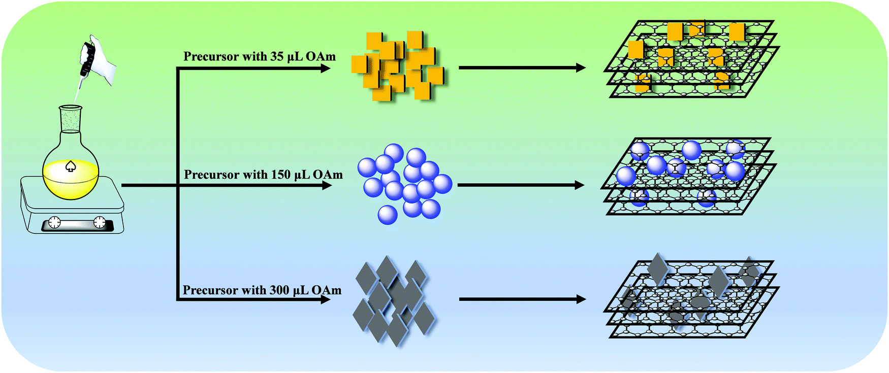 | ||
| Scheme 1 Synthesis of hybrid lead halide perovskite NC and the perovskite NC/graphite nanocomposite. | ||
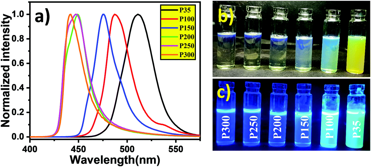 | ||
| Fig. 1 (a) The emission spectra with tunability of P35 to P300 (λexc = 415 nm). Images of P35 to P300 samples (b) under visible light and (c) under UV (365 nm) light radiation. | ||
To obtain more insight into the structure of the crystalline materials and the graphite composite, a concentrated solution of MAPbBr3 is deposited on a glass substrate and X-ray diffraction patterns were measured (Fig. 2). The diffraction peaks of MAPbBr3 perovskite nanocrystals observed at 2θ values of 15.38°, 21.63°, 30.61°, 34.25°, 43.60°, and 46.41° correspond to the (010), (011), (020), (021), (022), and (122) planes. The X-ray diffraction pattern shows the pure cubic face of MAPbBr3 (COD no. 1545320) with the Pm![[3 with combining macron]](https://www.rsc.org/images/entities/char_0033_0304.gif) m space group.44 The crystal planes of the PNCs/graphite composite shifted towards a low theta value compared to those of pristine MAPbBr3, and the FWHM values of the composite peaks also increase. Enlarged areas of the peaks around ∼15° and ∼30° are shown in Fig. S2 in the ESI.† Although the change in theta value and FWHM is significantly very small, it shows the interaction of graphite with MAPbBr3. Details of peak shifting and change in FWHM value are shown in a tabular form in the ESI,† in Table S1. The intense peak in Fig. 2 around 26.7° corresponding to the (003) plane in the composite spectrum shows the presence of graphite (COD no. 1200018).45
m space group.44 The crystal planes of the PNCs/graphite composite shifted towards a low theta value compared to those of pristine MAPbBr3, and the FWHM values of the composite peaks also increase. Enlarged areas of the peaks around ∼15° and ∼30° are shown in Fig. S2 in the ESI.† Although the change in theta value and FWHM is significantly very small, it shows the interaction of graphite with MAPbBr3. Details of peak shifting and change in FWHM value are shown in a tabular form in the ESI,† in Table S1. The intense peak in Fig. 2 around 26.7° corresponding to the (003) plane in the composite spectrum shows the presence of graphite (COD no. 1200018).45
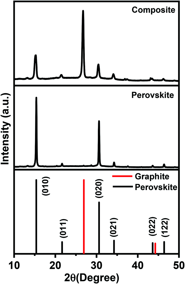 | ||
| Fig. 2 XRD spectra of pristine perovskite and the PNCs/graphite composite. | ||
Scanning electron microscopy (SEM) and transmission electron microscopy (TEM) were performed to understand the morphology of these nanocrystals and the nanocomposite morphological properties.
Firstly, the morphology of the MAPbBr3 and its evolution with the ligand ratio was investigated by FE-SEM as shown in Fig. 3a-l, which reveals that the nanocrystals are successfully fabricated onto the surface of graphite sheets. The morphology of the perovskite particles was controlled by changing the ligand concentrations in the reaction medium. SEM images of the perovskite and perovskite-graphite composite at different scale bars are shown in Fig. S3.1–S3.5 (ESI†). The SEM image of graphite is also incorporated in Fig. S3.6 (ESI†). The particles transformed from cubes to rhombus-shape as the concentration of oleyl amine was increased. The self-aggregation phenomenon is taken into account, while considering the development of nanoparticles.
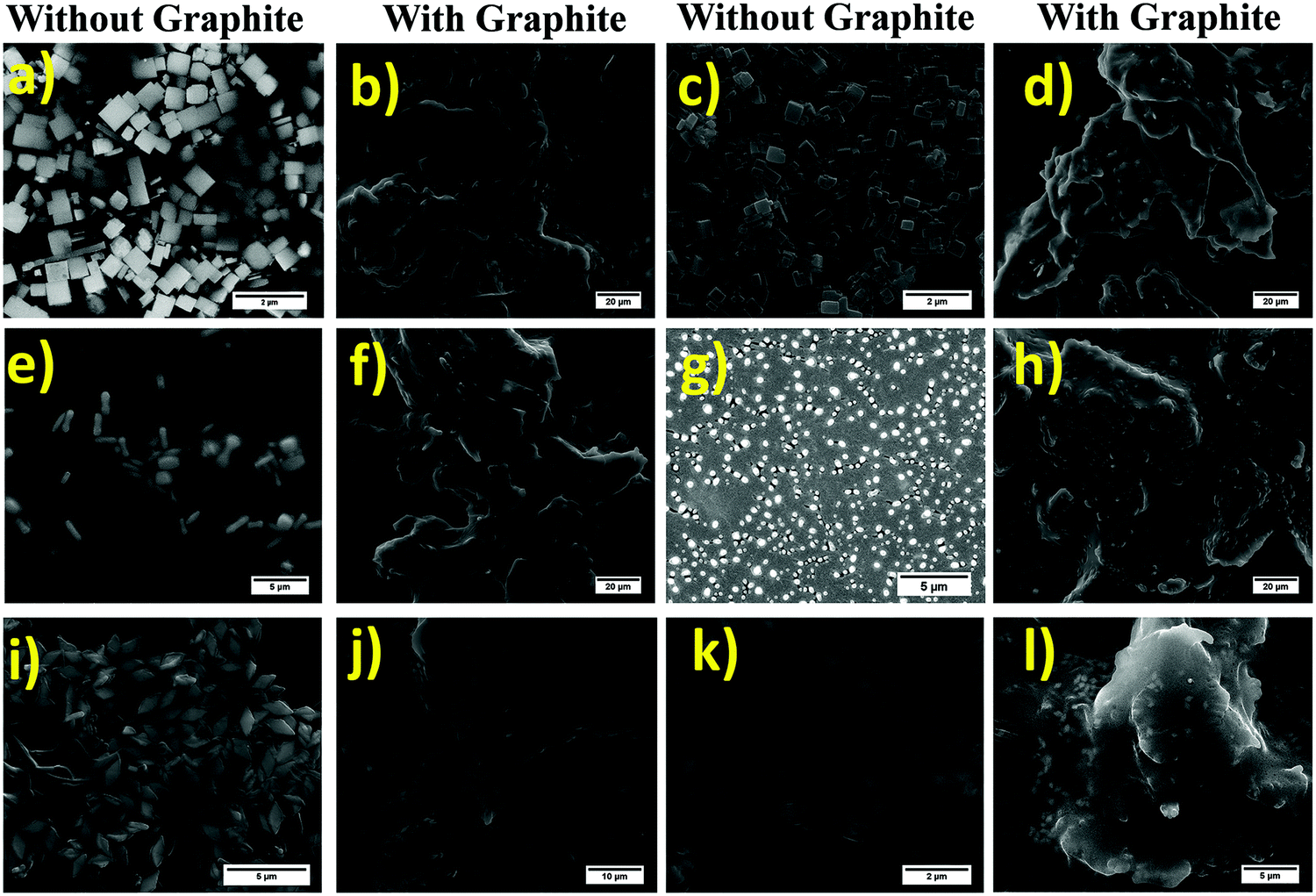 | ||
| Fig. 3 SEM images of pristine perovskites and corresponding graphite-perovskite composites: (a) P35, (b) P35@G, (c) P100, (d) P100@G, (e) P150, (f) P150@G, (g) P200, (h) P200@G, (i) P250, (j) P250@G, (k) P300, and (l) P300@G. | ||
To have a better understanding of the graphite-wrapped perovskite nanocrystals, cross-sectional images of the perovskites and the perovskite-graphite composites are displayed in Fig. S4.1–S4.3 (ESI†). The cross-sectional images demonstrate that the nanocrystals are successfully wrapped with the graphite sheets. TEM studies further reveal that at a lower concentration of ligands, the seeding of nanoparticles occurs. Then, overgrowth of these crystal seeds produces different self-assembled 2D nanoplates depending upon the ligand concentration, as shown in Fig. 4a. On the other hand, a higher concentration of ligand results in quantum dots of less than 5 nm (Fig. 4d). The selected area electron diffraction (SAED) pattern of the nanoparticles exhibits high crystallinity of the materials, as presented in Fig. 4b and e. Simultaneously, we have calculated the corresponding planes obtained from the SAED patterns. Planes calculated from SAED resemble the corresponding XRD planes. Fig. 4c and f show the particle size distribution of 10–40 nm, and 0.5–4.5 nm with the average particle size of ∼22 nm and ∼3 nm for the P35 and P300 samples, respectively.
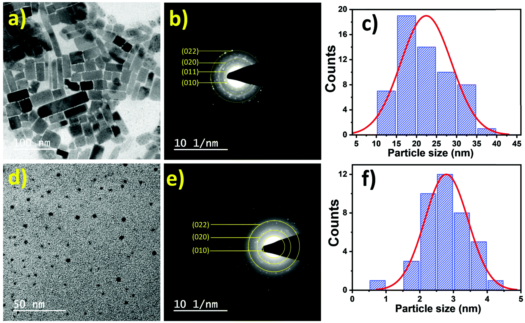 | ||
| Fig. 4 (a) TEM image, (b) SAED pattern and (c) size distribution curve of P35. (d) TEM image, (e) SAED pattern and (f) size distribution curve of P300. | ||
X-ray photoelectron spectroscopy (XPS) was further used to investigate the binding energy changes of the Br and Pb atomic environments. A survey scan (Fig. S5, ESI†) confirms the presence of all elements including C, N, Pb, and Br in the pristine and composite perovskite. The Pb and Br peaks of the composite are observed to shift toward higher binding energy. Fig. 5a displays the peaks corresponding to Br 3d5/2 and Br 3d3/2 with binding energies at 68.3 and 69.3 eV, respectively, for the pristine perovskite, while Br 3d5/2 and Br 3d3/2 in the composite have values at 68.6, and 69.6 eV. Similarly, Fig. 5b reveals the peaks corresponding to Pb 4f5/2 and Pb 4f7/2 with binding energies at 143.3 and 138.4 eV, respectively, for the pristine perovskite. On the other hand, the composite with graphite has values at 143.6, and 138.8 eV for Pb 4f5/2 and Pb 4f7/2, respectively. The change in binding energy corroborates the interaction between the perovskite and the composite.
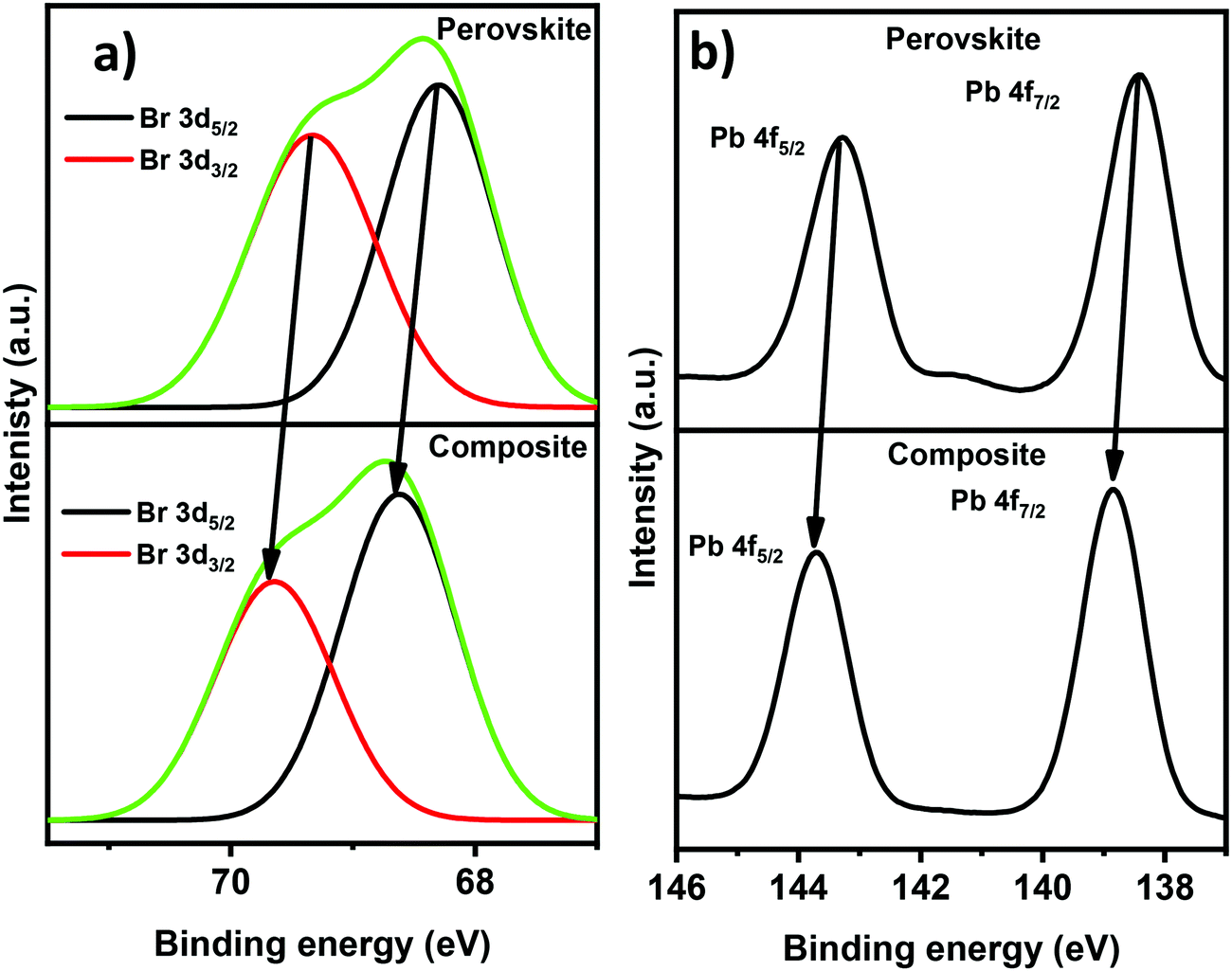 | ||
| Fig. 5 XPS narrow scans of (a) Br 3d and (b) Pb 4f. | ||
We performed a TGA experiment on PNC and its corresponding composite part. Fig. S6 (ESI†) displays the TGA spectra with a decrease in relative mass with temperature. The first mass-loss step starts from 280 °C to 380 °C where the mass percentage decreased from 100 to 76%. This step corresponds to the degradation of MABr (molar mass: MABr = 111.97 g mol−1). In the second step, mass loss starts from 470 °C, and this mass-loss step corresponds to PbBr2 (PbBr2 = 367.05 g mol−1). Similarly, when we performed TGA for the composite part degradation takes place in a similar manner to that of the pristine perovskite. Here we can conclude that before 250 °C, there is no mass loss in either the pristine perovskite or in the composite part, which is in good accordance with the literature.46
Furthermore, we have calculated the absolute PLQY values of all the samples with varying amounts of graphite solution (detail in Fig. S7, and Table S2, ESI†). The PLQY values are 51, 53, 29, 26, 16, and 5 for P35, P100, P150, P200, P250, and P300, respectively. As we increased the amount of graphite solution the PLQY value decreased for each sample.
The emission of PNC is quenched after the formation of nanocomposites. The broad emission band along with the quenching of this emission in the graphite composite leads to the hypothesis that the CTEs are formed at the heterostructure interfaces (Scheme S1, ESI†). To further understand the formation of CTEs and the charge transfer, we have performed fluorescence titrations of P35 to P300 in which a graphite solution (0.6% w/v in chloroform) was added gradually to the nanocrystals, which are shown in Fig. 6 and Fig. S8 (ESI†).
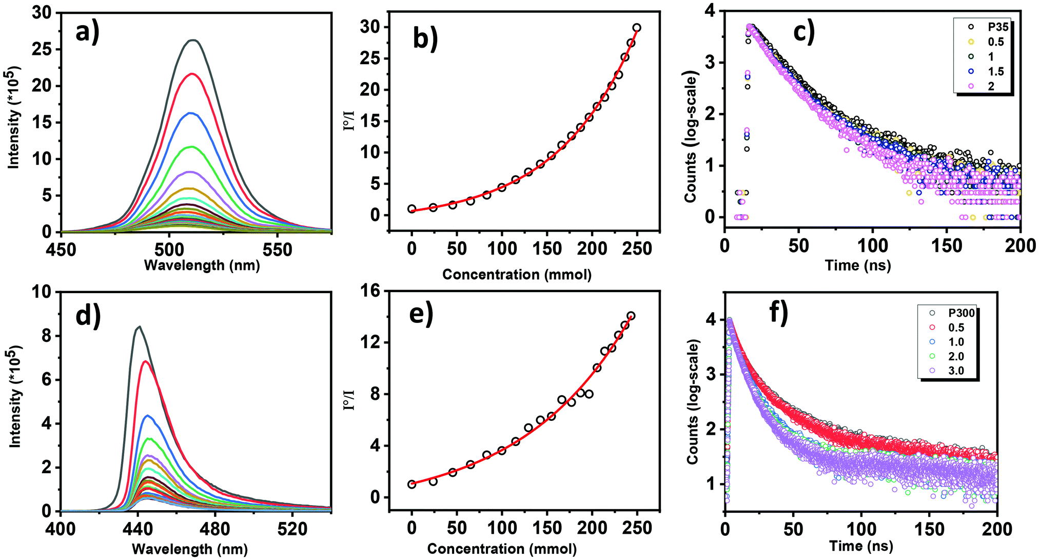 | ||
| Fig. 6 For P35: (a) photoluminescence (PL) quenching with graphite, λexc = 415 nm. (b) Change in PL intensity with respect to the concentration of graphite. (c) TCSPC (laser used = 405 nm). For P300: (d) photoluminescence (PL) quenching with graphite, λexc = 415 nm. (e) Change in PL intensity with respect to the concentration of graphite. (f) TCSPC (laser used = 405 nm). | ||
A continuous decrease in the emission evidenced the charge transfers from P35 and P300 to graphite, as noticed in Fig. 6a and d. Similarly, Fig. S7(a–d) (ESI†) correspond to the fluorescence quenching spectra for the samples of P100, P150, P200, and P250. Corresponding Stern–Volmer plots show non-linear behavior for P35 and P300 (Fig. 5b, e, and Fig. S7e–h (ESI†), respectively, for P100, P150, P200, and P250). Non-linear behavior is evident for both static and dynamic quenching of the perovskite.40,47 The concentration dilution effect was verified and is shown in Fig. S9 (ESI†).
To understand the charge transfer exciton behavior, time-correlated single-photon counting (TCSPC) studies are performed to observe the decay lifetime with the addition of graphite solution. In Fig. 6, the broad emission band peak at 512 nm shows a prolonged lifetime of nearly 25 ns. In general, the lifetime of charge-transfer excitons is observed by the electron–hole recombination rates directed by the Coulomb attraction force.
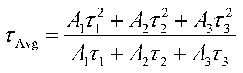
We should note that CTEs demonstrate various lifetimes when the electrons and holes are located on different energetic structures where the Coulombic attraction is changed by the local dielectric background. Emission decays of PNCs P35 and P300 at various ratios of PNC:graphite are presented in Fig. 6c and f, respectively. The decay could be fitted to the biexponential model for P35 and triexponential for P300. The fitting parameters are shown in Table 1. The average emission lifetime decreases with an increase in the ratio of PNC:graphite, which is in agreement with the steady-state quenching trend. The rapid electron injection process is responsible for a shorter lifetime than intrinsic excitons in semiconducting materials. We have observed a drastic change for the long component lifetime τ2, while there is no significant change in the short component τ1 (Table 1) for sample P35. These observations suggest that charge transfer takes place predominantly in the presence of graphite solution. The following formula is used to calculate the average lifetime of the perovskite nanocrystal.
| Graphite solution amount | A 1 | A 2 | A 3 | τ 1 | τ 2 | τ 3 | τ Avg(ns) |
|---|---|---|---|---|---|---|---|
| P35 | |||||||
| 0 mL | 91.75 | 8.25 | — | 13.17 | 56.65 | — | 25 |
| 0.5 mL | 85.75 | 14.25 | — | 11.03 | 36.44 | — | 20 |
| 1.0 mL | 81.24 | 18.76 | — | 10.04 | 32.47 | — | 19 |
| 1.5 mL | 84.30 | 15.70 | — | 10.68 | 33.78 | — | 19 |
| 2.0 mL | 82.95 | 17.05 | — | 9.9 | 28.9 | — | 17 |
| P300 | |||||||
| 0 mL | 927.34 | 7276.50 | 3601.30 | 24.60 | 6.43 | 1.49 | 12 |
| 0.5 mL | 1091.90 | 7275.40 | 2828 | 22.04 | 6.11 | 1.48 | 11 |
| 1.0 mL | 6342.30 | 4488.50 | 888.70 | 5.28 | 0.95 | 15.72 | 8 |
| 1.5 mL | 424.73 | 7743.70 | 4109.20 | 19.42 | 4.46 | 1.07 | 7 |
| 2.0 mL | 7633.30 | 411.53 | 4037.50 | 5.44 | 18.82 | 1.07 | 7 |
The possible mechanism for the emission quenching of PNCs is energy transfer or electron transfer, or both. Here the energy transfer process may be ruled out because the absorption spectrum of graphite and the emission spectrum of PNC are negligible (Fig. S10 in ESI†). The only possible mechanism is the electron transfer from PNC to graphite. To investigate the dynamic behavior of charge transfer excitons, we have conducted pump–probe transient absorption spectroscopy on the pristine sample coupled with the nanocomposite. Herein, we have prepared two different compositions for transient absorption spectroscopy (TAS) investigations. Firstly, P35 and the corresponding graphite composite P35@G, and the second one is P300 and the corresponding graphite composite P300@G. Ultrafast transient absorption spectroscopy is based on the pump–probe technique where the experiment is progressed by excitation of molecules at a specific wavelength (called a pump) by a Ti:sapphire laser.
A weak pulse passing through the delay stage (called a probe) is used to investigate the dynamics of excited carriers. These ultrafast investigations are done using an oscillator (Micra), an amplifier (Coherent Legend), an optical parametric amplifier (OPA), and a spectroscopy system (Helios). The coherent legend has a fundamental beam of 800 nm (divided into two parts) with a repetition rate of 1 kHz, 35–45 fs pulse width, and average energy of 3–4 W. OPA generating tunable femtosecond (240–2600 nm) pulses with a pulse width of 70 fs at the sample is used to stimulate the sample using the pump pulse. Surface Xplorer software and Origin 9.1 are utilized to accomplish fitting the data for analysis. The transient absorption behavior of MAPbBr3 and after adding graphite was observed by modulating the pump laser in the excited state of the electron in the fs-ns time scale.
The photoinduced absorption, stimulation, and photoinduced bleaching are indicated in the spectral window of the TA spectra between 400 and 800 nm. Here, P35 and P35@G were stimulated at 350 nm and 450 nm with an average pump power of 1 mW. The white light continuum probe pulse (delayed) versus pump pulse displays the absorption variations (ΔA) with wavelength and time. Fig. 7(a and b) illustrate the transient absorption spectra of P35. Here we get the ground state bleaching at ∼480 nm, PIA at ∼530 nm, and SE at ∼550 to 800 nm probe delay wavelengths. The spectral characteristics after adding graphite demonstrate some modified signature, graphite added to P35 quenches the bond energy and bond wavelengths as displayed in Fig. 7(c and d). The TAS characteristics indicate a wide spectral signal from 533 nm to 700 nm for the pristine compound (Fig. 7b). Interestingly this wide signal vanishes in the composite, suggesting the distinct dynamic behavior in the composite (Fig. 7d). A photobleaching signal is found with a growing component in the pristine sample demonstrating the ground state absorption characteristic. On the contrary, the growing component at the shorter time scale is eliminated with a quick decline in the composite clearly demonstrating the efficient charge transfer in the composite, as illustrated in Fig. 7b and d. A significant signal from 503 nm to 533 nm in Fig. 7b is found, which entirely vanishes in the nanocomposite. By considering the fact that the excitons are evolved into the bleaching signals in the pristine sample, it may have a chance to contribute to the production of CTE as illustrated by the rapid decay kinetics in Fig. 7a and c. Therefore, the dynamics of excitons contain two processes. Firstly, an intrinsic exciton is created, which slowly fades with long decay kinetics. Secondly, the surface excitons readily transfer the charges to the nanocomposite showing effective creation of charge-transfer excitons at the interface. Similarly, we have done transient absorption spectroscopy investigations with the P300 sample and we found identical findings as for P35, as shown in Fig. S11 (ESI†). Details of TAS investigations for both the samples have been put in Table S3 (ESI†).
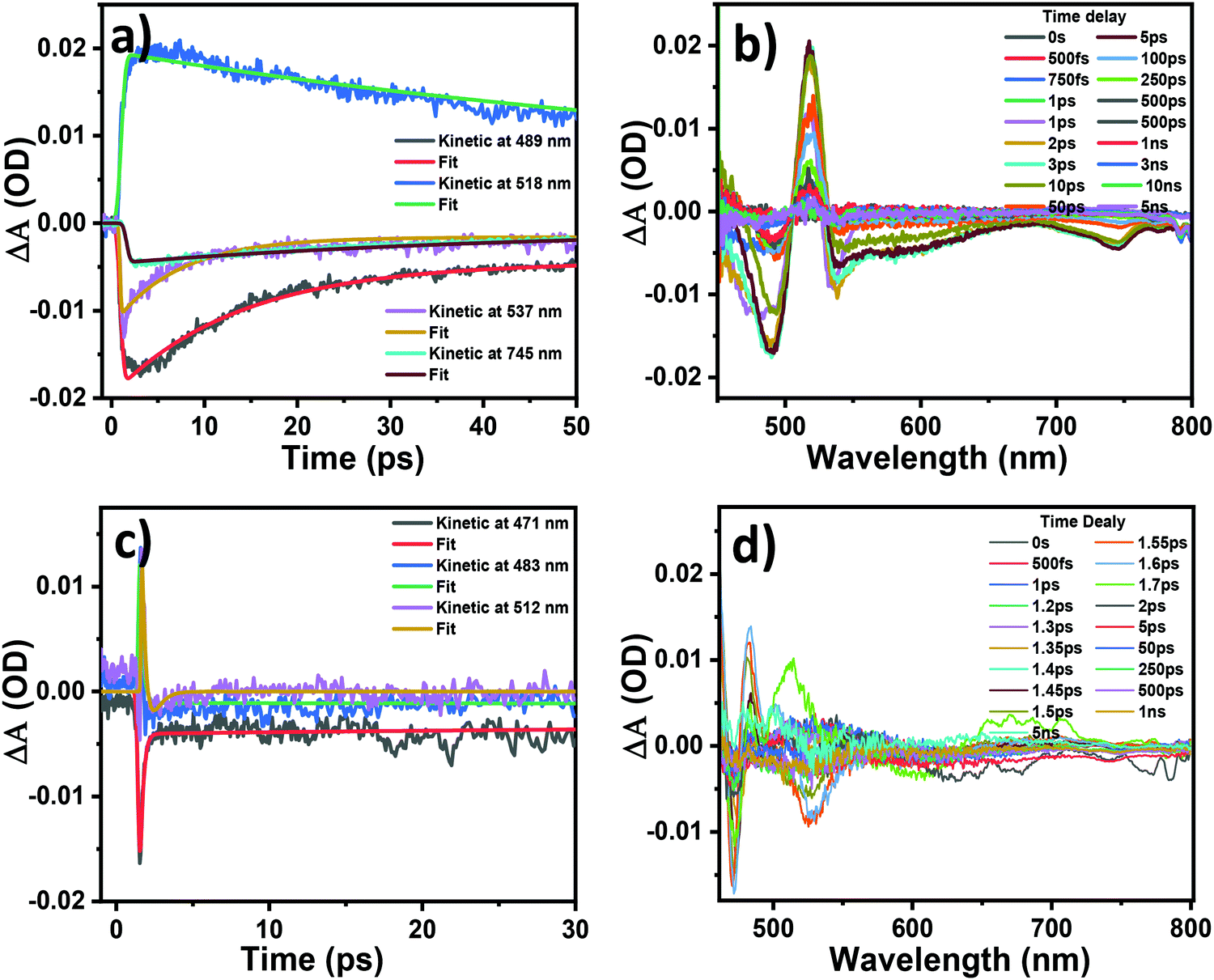 | ||
| Fig. 7 The TAS spectra of (a) and (b) P35, and (c) and (d) P35@G. | ||
Conclusions
In summary, we have successfully synthesized perovskite nanocrystals of diverse shapes to examine the charge transfer potential with unfunctionalized graphite sheets. We have demonstrated that PNCs reasonably behave as an excellent electron donor when coupled with an acceptor such as graphite. Herein, we established effective charge transfer exciton creation, which efficiently transfers electrons from PNCs to graphite. TEM investigations demonstrate that self-aggregation happens with decreasing ligand concentration to generate different morphologies, while high ligand concentration gives small quantum dots. These nanocrystals have effectively bonded to the surface of the graphite sheets. This leads to the possibility that CTEs are formed in PNC graphite composites and provide opportunities to undertake sophisticated optoelectronics studies on the nanocomposite of PNC and graphite sheets.Author contributions
Gaurav Kumar Nim: investigation, methodology, and writing – original draft. Sukanya Ghosh: writing – review and editing. Saurabh K Saini: transient absorption spectroscopy studies and editing. Mahesh Kumar: writing – review and editing. Prasenjit Kar: supervision, writing – review and editing.Declaration
The authors declare that they have no known competing financial interests or personal relationships that could have influenced the work reported in this paper.Conflicts of interest
The authors declare no conflict of interest.Acknowledgements
The authors gratefully acknowledge financial support for this work from Science and Engineering Research Board (CRG/2020/000702), New Delhi, India. The authors also acknowledge the Institute Instrumentation Centre (IIC) of IIT Roorkee for providing the instrumentation facilities. GKN and SKS acknowledge UGC, India, for their doctoral fellowships. SG acknowledges MoE, India, for her doctoral fellowship.References
- (a) H. C. Wang, S. Y. Lin, A. C. Tang, B. P. Singh, H. C. Tong, C. Y. Chen, Y. C. Lee, T. L. Tsai and R. S. Liu, Angew. Chem., Int. Ed., 2016, 55, 7924–7929 CrossRef CAS PubMed; (b) P. Bansal, Y. Khan, G. K. Nim and P. Kar, Chem. Commun., 2018, 54, 3508–3511 RSC; (c) S. Ghosh, G. K. Nim, P. Bansal and P. Kar, J. Colloid Interface Sci., 2021, 582, 1223–1230 CrossRef CAS PubMed.
- (a) D. Zhang, S. W. Eaton, Y. Yu, L. Dou and P. Yang, J. Am. Chem. Soc., 2015, 137, 9230–9233 CrossRef CAS; (b) A. K. Sharma, P. Bansal, G. K. Nim and P. Kar, Part. Part. Syst. Charact., 2019, 36, 1900328 CrossRef CAS; (c) S. Ghosh, G. K. Nim, H. Shankar and P. Kar, New J. Chem., 2021, 45, 22691–22696 RSC.
- H. Lin, C. Zhou, M. Chaaban, L.-J. Xu, Y. Zhou, J. Neu, M. Worku, E. Berkwits, Q. He, S. Lee, X. Lin, T. Siegrist, M.-H. Du and B. Ma, ACS Mater. Lett., 2019, 1, 594–598 CrossRef CAS.
- A. Manzi, Y. Tong, J. Feucht, E.-P. Yao, L. Polavarapu, A. S. Urban and J. Feldmann, Nat. Commun., 2018, 9, 1518 CrossRef.
- (a) J. A. Christians, P. A. Miranda Herrera and P. V. Kamat, J. Am. Chem. Soc., 2015, 137, 1530–1538 CrossRef CAS PubMed; (b) G. K. Nim, P. Bansal and P. Kar, ACS omega, 2019, 4, 15678–15683 CrossRef CAS.
- Y. Kim, E. Yassitepe, O. Voznyy, R. Comin, G. Walters, X. Gong, P. Kanjanaboos, A. F. Nogueira and E. H. Sargent, ACS Appl. Mater. Interfaces, 2015, 7, 25007–25013 CrossRef CAS.
- L. Dou, A. B. Wong, Y. Yu, M. Lai, N. Kornienko, S. W. Eaton, A. Fu, C. G. Bischak, J. Ma, T. Ding, N. S. Ginsberg, L. W. Wang, A. P. Alivisatos and P. Yang, Science, 2015, 349, 1518–1521 CrossRef CAS.
- D. P. McMeekin, G. Sadoughi, W. Rehman, G. E. Eperon, M. Saliba, M. T. Hörantner, A. Haghighirad, N. Sakai, L. Korte and B. Rech, Science, 2016, 351, 151–156 CrossRef CAS PubMed.
- N. J. Jeon, J. H. Noh, W. S. Yang, Y. C. Kim, S. Ryu, J. Seo and S. I. Seok, Nature, 2015, 517, 476–480 CrossRef CAS PubMed.
- L. Song, X. Guo, Y. Hu, Y. Lv, J. Lin, Z. Liu, Y. Fan and X. Liu, J. Phys. Chem. Lett., 2017, 8, 4148–4154 CrossRef CAS.
- P. Gui, Z. Chen, B. Li, F. Yao, X. Zheng, Q. Lin and G. Fang, ACS Photonics, 2018, 5, 2113–2119 CrossRef CAS.
- NREL efficiency chart Available: https://www.nrel.gov/pv/insights/assets/pdfs/cell-pv-eff-emergingpv.pdf, 2021.
- X.-Y. Zhu, Q. Yang and M. Muntwiler, Acc. Chem. Res., 2009, 42, 1779–1787 CrossRef CAS.
- A. E. Jailaubekov, A. P. Willard, J. R. Tritsch, W.-L. Chan, N. Sai, R. Gearba, L. G. Kaake, K. J. Williams, K. Leung, P. J. Rossky and X.-Y. Zhu, Nat. Mater., 2013, 12, 66–73 CrossRef CAS PubMed.
- L. Zhao, Y. L. Lin, H. Kim, N. C. Giebink and B. P. Rand, ACS Energy Lett., 2018, 3, 2708–2712 CrossRef CAS.
- T. H. Han, H. Kim, S. J. Kwon and T. W. Lee, Mater. Sci. Eng., R, 2017, 118, 1–43 CrossRef.
- T. H. Han, Y. Lee, M. R. Choi, S. H. Woo, S. H. Bae, B. H. Hong, J. H. Ahn and T. W. Lee, Nat. Photonics, 2012, 6, 105–110 CrossRef CAS.
- H. K. Seo, H. Kim, J. Lee, M. H. Park, S. H. Jeong, Y. H. Kim, S. J. Kwon, T. H. Han, S. Yoo and T. W. Lee, Adv. Mater., 2017, 29, 1605587 CrossRef PubMed.
- T. H. Han, S. J. Kwon, N. Li, H. K. Seo, W. Xu, K. S. Kim and T. W. Lee, Angew. Chem., Int. Ed., 2016, 55, 6197–6201 CrossRef CAS PubMed.
- S. J. Kwon, T. H. Han, T. Y. Ko, N. Li, Y. Kim, D. J. Kim, S. H. Bae, Y. Yang, B. H. Hong, K. S. Kim, S. Ryu and T. W. Lee, Nat. Commun., 2018, 9, 2037 CrossRef.
- T. H. Han, M. H. Park, S. J. Kwon, S. H. Bae, H. K. Seo, H. Cho, J. H. Ahn and T. W. Lee, NPG Asia Mater., 2016, 8, 303 CrossRef.
- H. Kim, S. H. Bae, T. H. Han, K. G. Lim, J. H. Ahn and T. W. Lee, Nanotechnology, 2014, 25, 014012 CrossRef CAS.
- Y. Zhu, G. Lai, J. Yi, T. Zhang, Y. Zhang, S. Wen and H. Zhou, J. Alloys Compd., 2021, 866, 158990 CrossRef CAS.
- I. Poli, U. Hintermair, M. Regue, S. Kumar, E. V. Sackville, J. Baker, T. M. Watson, S. Eslava and P. J. Cameron, Nat. Commun., 2019, 10, 2097 CrossRef.
- S. K. Yadav, Mater. Chem. Phys., 2021, 268, 124709 CrossRef CAS.
- D. Bogachuk, R. Tsuji, D. Martineau, S. Narbey, J. P. Herterich, L. Wagner, K. Suginuma, S. Ito and A. Hinsch, Carbon, 2021, 178, 10–18 CrossRef CAS.
- M. Xu, Y. Rong, Z. Ku, A. Mei, T. Liu, L. Zhang, X. Li and H. Han, J. Mater. Chem. A, 2014, 2, 8607–8611 RSC.
- S. Gholipour, J. Pablo, C. Baena, K. Domanski, T. Matsui, L. Steier, F. Giordano, F. Tajabadi, W. Tress, M. Saliba, A. Abate, A. Morteza Ali, N. Taghavinia, M. Grätzel and A. Hagfeldt, Adv. Energy Mater., 2016, 6, 1601116 CrossRef.
- A. Mei, X. Li, L. Liu, Z. Ku, T. Liu, Y. Rong, M. Xu, M. Hu, J. Chen, Y. Yang, M. Grätzel and H. Han, Science, 2014, 345, 295–298 CrossRef CAS.
- R. Aepuru, C. N. Rao, R. Udayabhaskar, D. Vennu, V. M. Gaikwad, V. Kumar, H. S. Panda, P. Aqueveque, P. Cao and R. V. Mangalaraja, J. Phys. Chem. C, 2020, 124, 26648–26658 CrossRef CAS.
- K. Leng, L. Wang, Y. Shao, I. Abdelwahab, G. Grinblat, I. Verzhbitskiy, R. Li, Y. Cai, X. Chi, W. Fu, P. Song, A. Rusydi, G. Eda, S. A. Maier and K. P. Loh, Nat. Commun., 2020, 11, 5483 CrossRef CAS PubMed.
- Q. Fang, Q. Shang, L. Zhao, R. Wang, Z. Zhang, P. Yang, X. Sui, X. Qiu, X. Liu, Q. Zhang and Y. Zhang, J. Phys. Chem. Lett., 2018, 9, 1655–1662 CrossRef CAS.
- W. Wen, W. Zhang, X. Wang, Q. Feng, Z. Liu and T. Yu, Small, 2021, 17, 2102461 CrossRef CAS.
- Y. Sheng, A. Zhao, L. Yu, S. Yuan, Y. Di, C. Liu, L. Dong and Z. Gan, Phys. Status Solidi B, 2020, 257, 2000198 CrossRef CAS.
- L. C. Schmidt, A. Pertegas, S. Gonzalez-Carrero, O. Malinkiewicz, S. Agouram, G. M. Espallargas, H. J. Bolink, R. E. Galian and J. PerezPrieto, J. Am. Chem. Soc., 2014, 136, 850–853 CrossRef CAS PubMed.
- S. Gonzalez-Carrero, R. E. Galian and J. Perez-Prieto, J. Mater. Chem. A, 2015, 3, 9187–9193 RSC.
- H. Huang, L. Polavarapu, J. A. Sichert, A. S. Susha, A. S. Urban and A. L. Rogach, NPG Asia Mater., 2016, 8, 328 CrossRef.
- Q. Zhang and Y. Yin, ACS Cent. Sci., 2018, 4, 668–679 CrossRef CAS PubMed.
- P. Bansal, X. Zhang, H. Wang, P. Kar and W. W. Yu, Nanoscale Adv., 2020, 2, 808 RSC.
- F. Haydous, J. M. Gardner and U. B. Cappel, J. Mater. Chem. A, 2021, 9, 23419–23443 RSC.
- X. Li, D. Yu, F. Cao, Y. Gu, Y. Wei, Y. Wu, J. Song and H. Zeng, Adv. Funct. Mater., 2016, 26, 5903–5912 CrossRef CAS.
- H. Huang, J. Raith, S. V. Kershaw, S. Kalytchuk, O. Tomanec, L. Jing, A. S. Susha, R. Zboril and A. L. Rogach, Nat. Commun., 2017, 8, 996 CrossRef PubMed.
- G. A. Elbaz, D. B. Straus, O. E. Semonin, T. D. Hull, D. W. Paley, K. Philip, J. S. Owen, C. R. Kagan and X. Roy, Nano Lett., 2017, 17, 1727–1732 CrossRef CAS PubMed.
- H. Lipson and A. R. Stokes, The structure of graphite, Proc. R. Soc. London, Ser. A, 1942, 181, 101–105 CAS.
- M. Kulbak, S. Gupta, N. Kedem, I. Levine, T. Bendikov, G. Hodes and D. Cahen, J. Phys. Chem. Lett., 2016, 7, 167–172 CrossRef CAS PubMed.
- J. Liu, Y. Zhong, P. Lu, Y. Hong, J. W. Y. Lam, M. Faisal, Y. Yu, K. Sing Wong and B. Z. Tang, Polym. Chem., 2010, 1, 426–429 RSC.
- Y. Wang, T. Wu, J. Barbaud, W. Kong, D. Cui, H. Chen, X. Yang and L. Han, Science, 2019, 365, 687–691 CrossRef CAS PubMed.
Footnote |
| † Electronic supplementary information (ESI) available. See DOI: https://doi.org/10.1039/d2nj01116f |
| This journal is © The Royal Society of Chemistry and the Centre National de la Recherche Scientifique 2022 |