 Open Access Article
Creative Commons Attribution 3.0 Unported Licence
Graphene assisted crystallization and charge extraction for efficient and stable perovskite solar cells free of a hole-transport layer
Ahmed Esmail
Shalan
ab,
Mustafa K. A.
Mohammed
 *c and
Nagaraj
Govindan
 d
d
aCentral Metallurgical Research and Development Institute (CMRDI), P. O. Box 87, Helwan, Cairo 11421, Egypt
bBCMaterials, Basque Center for Materials, Applications and Nanostructures, Martina Casiano, UPV/EHU Science Park, Barrio Sarriena s/n, Leioa 48940, Spain
cTechnical Engineering College, Middle Technical University, Baghdad, Iraq. E-mail: mustafa_kareem97@yahoo.com; Tel: +9647719047121
dDepartment of Physics, Periyar University, P.G Extension Center, Dharmapuri, Tamil Nadu, India
First published on 22nd January 2021
Abstract
In recent times, perovskite solar cells (PSCs) have been of wide interest in solar energy research, which has ushered in a new era for photovoltaic power sources through the incredible enhancement in their power conversion efficiency (PCE). However, several serious challenges still face their high efficiency: upscaling and commercialization of the fabricated devices, including long-term stability as well as the humid environment conditions of the functional cells. To overcome these obstacles, stable graphene (G) materials with tunable electronic features have been used to assist the crystallization as well as the charge extraction inside the device configuration. Nonetheless, the hole transport layer (HTL)-free PSCs based on graphene materials exhibit unpredictable results, including a high efficiency and long-term stability even in the conditions of an ambient air atmosphere. Herein, we combine graphene materials into a mesoporous TiO2 electron transfer layer (ETL) to improve the coverage and crystallinity of the perovskite material and minimize charge recombination to augment both the stability and efficiency of the fabricated mixed cation PSCs in ambient air, even in the absence of a HTL. Our results demonstrate that an optimized PSC in the presence of different percentages of graphene materials displays a PCE of up to 17% in the case of a G:TiO2 ETL doped with 1.5% graphene. With this coverage and crystallinity amendment approach, we show hysteresis-free and stable PSCs, with less decomposition after ∼3000 h of storage under a moist ambient atmosphere. This work focuses on the originalities of the materials, expenses, and the assembling of stable and effective perovskite solar cells.
1. Introduction
Solution-processed perovskite solar cells (PSCs) dependent on an organometal trihalide have become promising candidates for third-generation solar cells and have been intensively focused on as an actual challenger to conventional silicon photovoltaics, attributable to their different advantages, including that they are cost-effective, easy to assemble and have high power conversion efficiencies.1–8The typical structural configuration of the PSC includes an absorber perovskite (PVK) layer sandwiched between electron and hole transfer layers (ETL and HTL) that is responsible for light harvesting and charge generation.9–15 However, the perovskite layer can provide dual functions and serve as a sensitizer as well as a hole transport material.16 Besides this, TiO2, as a semiconducting oxide, has been extensively applied as an ETL in solar cells to deliver effective electron extraction.17–20 The incorporation of carbon nano-object traces, like graphene materials in the structure of semiconductor materials, are considered as one possible direction, advancing the charge collection efficiency of the fabricated devices.21,22 TiO2 has appropriate characteristics, such as a wide bandgap energy, high exciton binding energy, high light absorption and high efficiency, low cost, and acceptable electron mobility.23 Inappropriate conduction band alignment and low conductivity of each layer are critical disadvantages.24 Consequently, additional efforts have been dedicated in these directions to enhance the performance of the stabilized devices. Graphene and other carbon nanomaterials are promising candidates for this objective.25–27 A monolayer of graphene and/or its derivatives with a honeycomb lattice have caused much fascination to engage them in solar cells for the reason that they serve as a rapid charge funnel.28–30
Predominantly, graphene materials can improve the conductivity and deliver a better band alignment between the different layers. Also, graphene has been applied as a dopant or interlayer in PSCs, in which it can improve the morphological and crystalline features of the PVK material, afford a proficient charge-extraction pathway and support electron collection from the PVK film to the ETL.31 Different researchers have studied the addition of graphene materials to different ETLs to augment charge injection and reduce the recombination process.32,33 However, the effect of graphene on the coverage and crystallinity of the perovskite layer as well as the long-term stability of PSCs have not been well investigated. Therefore, it is essential to additionally discover the positive effect of graphene materials in the structure, efficiency and stability of the fabricated cells.
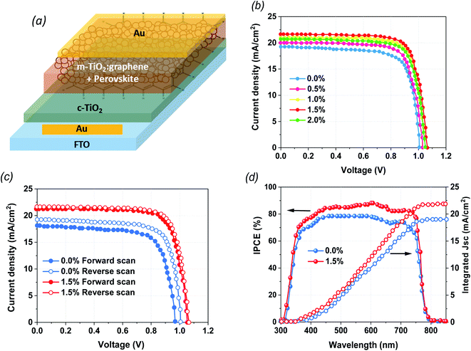
Herein, we assembled mixed cation HTL-free PSCs in ambient air based on both bare TiO2 and TiO2 doped with different molar ratios of graphene materials. Graphene materials are incorporated into the mesoporous TiO2 ETL to enhance the coverage and crystallinity of the perovskite material and minimize charge recombination to boost both the stability and efficiency of the fabricated mixed cation PSCs in ambient air, even in the absence of a HTL. The gained PCE of the assembled PSCs is improved from 12.48% to reach almost 16.75% with a smaller hysteresis effect after the graphene addition to the TiO2 ETL. With this coverage and crystallinity amendment approach, the devices demonstrate less decomposition after ∼3000 h of storing in a moist ambient environment. This study affords a practical way to acquire stable and efficient mixed cation PSCs in ambient air and depicts the essential role of graphene in modifying the interfacial contact between TiO2 and PVK, as well as assembling stable and effective perovskite solar cells.
2. Experimental
2.1. Chemicals and reagents
Unless otherwise stated, all the materials were purchased from Merck and used as received. N,N-Dimethylformamide (DMF, 99.8%), formamidinium iodide (FAI, 99%), and methylammonium bromide (MABr, 99%) were provided by Dyesol. Isopropanol (IPA, 99.5%), lead iodide (PbI2), titanium diisopropoxide (TAA), and m-TiO2 were ordered from Sigma-Aldrich. Graphene powder (purity ∼99%, sheet thickness ≤10 nm) was provided by Alibaba.2.2. Device fabrication
All the operations were performed under ambient air conditions and without any control method. The patterned-FTO glasses were successively cleaned using a detergent solution, deionized water, IPA, and ethanol in an ultrasonic bath for 5 min (every step). The FTO substrates were dried in an oven at 80 °C for 20 min and treated with an ultraviolet (UV)-ozone cleaner for 15 min before use. A compact-TiO2 (c-TiO2) (0.18 M TAA in ethanol) was spin-coated at 4000 rpm for 45 s and sintered at 300 °C for 10 min. Then, the mixtures of G/TiO2 (0.0%, 0.5%, 1.0%, 1.5%, and 2.0%) were spun at 5000 rpm for 35 seconds by employing a TiO2 paste dispersed in ethanol at 1![[thin space (1/6-em)]](https://www.rsc.org/images/entities/char_2009.gif) :
:![[thin space (1/6-em)]](https://www.rsc.org/images/entities/char_2009.gif) 6 and baked at 425 °C for 15 min. The ETLs were immersed in a 0.025 M titanium tetrachloride aqueous solution at 70 °C for 20 min, then dried with N2 gas and again baked at 425 °C for 20 min. For the mixed cation perovskite, 0.458 g of lead iodide (PbI2) and 0.065 g of DMSO were added to 0.5 g of DMF and mixed for 1 h at ambient conditions. The FAI
6 and baked at 425 °C for 15 min. The ETLs were immersed in a 0.025 M titanium tetrachloride aqueous solution at 70 °C for 20 min, then dried with N2 gas and again baked at 425 °C for 20 min. For the mixed cation perovskite, 0.458 g of lead iodide (PbI2) and 0.065 g of DMSO were added to 0.5 g of DMF and mixed for 1 h at ambient conditions. The FAI![[thin space (1/6-em)]](https://www.rsc.org/images/entities/char_2009.gif) :
:![[thin space (1/6-em)]](https://www.rsc.org/images/entities/char_2009.gif) MABr mixture (0.05 g
MABr mixture (0.05 g![[thin space (1/6-em)]](https://www.rsc.org/images/entities/char_2009.gif) :
:![[thin space (1/6-em)]](https://www.rsc.org/images/entities/char_2009.gif) 0.005 g) was dispersed in 1 mL of the IPA solvent. The PbI2 precursor was spun onto the G:TiO2 ETL at 4000 rpm for 20 s. FAI:MABr mixtures were deposited on top of the PbI2 film at 5000 rpm for 40 s and then annealed on the hotplate at 120 °C for 15 min. Finally, 80 nm of a Au counter electrode was evaporated to complete the HTL-free device fabrication.
0.005 g) was dispersed in 1 mL of the IPA solvent. The PbI2 precursor was spun onto the G:TiO2 ETL at 4000 rpm for 20 s. FAI:MABr mixtures were deposited on top of the PbI2 film at 5000 rpm for 40 s and then annealed on the hotplate at 120 °C for 15 min. Finally, 80 nm of a Au counter electrode was evaporated to complete the HTL-free device fabrication.
2.3. Characterization
The morphological properties of the PVK films were measured by scanning electron microscopy (SEM, TESCAN). The crystalline nature of the perovskite was measured using XRD analysis (Bruker, D8 Advance). The optical characteristics of perovskites were measured via photoluminescence (PL) spectroscopy (Varian Cary Eclipse Fluorescence) and UV-visible spectroscopy (Ocean Optics). Current density–voltage (J–V) characteristics of the devices were determined by a Keithley Model 2400 under 100 mW cm−2 (AM 1.5G one sun) illumination. The PSCs have an active area of 0.07 cm2. The charge generation and collection were monitored by an IPCE system (BunkoukeikiCEP-1500). The Nyquist plots were measured via electrochemical impedance spectroscopy (EIS, electrochemical workstation, Zennium 400147). The time-resolved PL (TRPL) was recorded at 760 nm employing excitation with a 478 nm light pulse from Delta Flex Fluorescence Lifetime System (Horiba Scientific Com.).3. Results and discussion
The structural configurations of the fabricated devices in the current study are illustrated in Fig. 1a. The mixed cation perovskite (PVK) layers were grown directly on the mixtures of G:TiO2 (0.0%, 0.5%, 1.0%, 1.5%, and 2.0%) photoelectrode films that work as ETLs via a two-step spin-coating deposition technique in ambient conditions. The architecture of FTO/c-TiO2/m-TiO2:graphene/perovskite/Au demonstrates the impact of graphene materials on the loss of a hole transport layer (HTL) in PSCs free of HTLs. After that, the devices were completed with thermally evaporated Au back contacts. In the current work, the essential role of graphene materials is to modify the crystallization of the perovskite film to improve the surface coverage as well as the interfacial contact between G/TiO2 and the PVK layer. Consequently, graphene materials have a valuable impact on lessening the instability of the PVK on top of the G:TiO2 film. To detect the efficiency of the fabricated devices, the photovoltaic (PV) parameters were checked through I–V measurements. The J–V curves of the optimized PSCs with altered molar ratios of graphene (0.0%, 0.5%, 1.0%, 1.5%, and 2.0%) in G:TiO2 as the ETLs were measured at reverse scan conditions under air mass 1.5 global (AM 1.5 G) conditions (Fig. 1b). The device with bare TiO2 and without the addition of graphene (reference cells) displays a PCE of 12.48%, whereas the addition of graphene materials to the composition of TiO2 with different molar ratios of G:TiO2 results in an augmentation in the overall efficiency. We find that G:TiO2 samples with 1.5% graphene are the optimal composition for PV performance. A maximum PCE of 16.75%, with Voc of 1.065 V, Jsc of 21.71 mA cm−2, and FF of 73.47% were detected for that composition. This improvement is accredited to the enhanced Voc and Jsc because of the higher conductivity and lower trap states in the G:TiO2. The addition of graphene weakens the reaction of MAI and TiO2, which could keep the long lifetime of the TiO2 layer. Besides this, the main characterization methods were carried out on 0.0% G:TiO2 and 1.5% G:TiO2 for the comparative study. We considered the hysteresis effect of the examined cells at the forward and reverse scans, which is obviously reduced in the case of 1.5% G:TiO2 based devices (Fig. 1c). The low hysteresis effect indicated for 1.5% G:TiO2 can be accredited to the better charge transfer and reduction of recombination because of a higher conductivity and lower trap states in the G:TiO2 layer. In addition, the validity of Jsc findings for the 0.0% G:TiO2 and 1.5% G:TiO2 samples was confirmed via external quantum efficiency measurements (Fig. 1d). The integrated Jsc values derived from the EQE data were 19.10 mA cm−2 and 21.60 mA cm−2, respectively, for the 0.0% G:TiO2 and 1.5% G:TiO2 PSCs, which are in decent alignment with the Jsc values gained from the J–V curves (Fig. 1b). Besides this, all the photovoltaic parameters of the fabricated HTL-free PSCs with a diverse amount of graphene (0.0%, 0.5%, 1.0%, 1.5%, and 2.0%) in G:TiO2 layer are listed in Table 1.| Device | V oc a (V) | J sc b (mA cm−2) | FFc (%) | PCEd (%) | |
|---|---|---|---|---|---|
| a V oc: open-circuit voltage. b Jsc: short-circuit current density. c FF: fill factor. d PCE: power conversion efficiency. | |||||
| 0.0% | Average | 0.975 | 18.67 | 63.49 | 11.55 |
| Best | 1.003 | 19.25 | 64.65 | 12.48 | |
| 0.5% | Average | 1.004 | 19.18 | 65.32 | 12.56 |
| Best | 1.024 | 20.01 | 66.29 | 13.58 | |
| 1.0% | Average | 1.012 | 20.02 | 68.27 | 13.83 |
| Best | 1.036 | 20.92 | 69.87 | 15.14 | |
| 1.5% | Average | 1.031 | 20.45 | 71.71 | 15.19 |
| Best | 1.065 | 21.71 | 73.47 | 16.75 | |
| 2.0% | Average | 1.012 | 19.85 | 67.13 | 13.48 |
| Best | 1.044 | 20.70 | 68.45 | 14.79 | |
The statistical analysis as well as the average photovoltaic parameters of 20 fabricated devices for each composition of G:TiO2 are shown in Fig. 2. The corresponding box chart plots of Jsc, Voc, and FF for the different amounts of graphene (0.0%, 0.5%, 1.0%, 1.5%, and 2.0%) in the G:TiO2 layer can be found in Fig. 2(a–d), representing a superb reproducibility with a limited variation. The highest parameters were detected for the device using TiO2 containing 1.5% graphene as an ETL, principally because of the highest Jsc value that is attributed to the greatest effectual interfacial charge transfer and the lowest carrier recombination, as affirmed from EIS measurements (see Fig. 4c).34,35
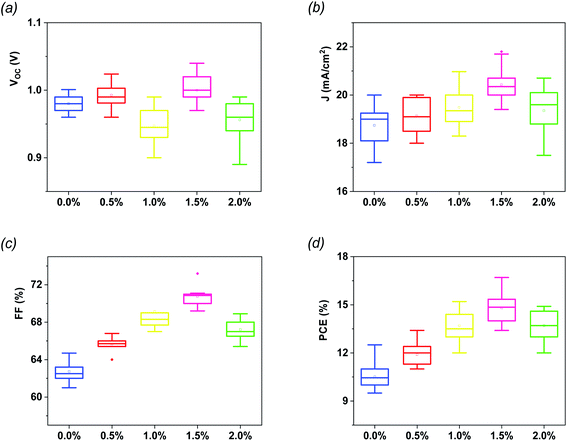 | ||
| Fig. 2 Statistical histograms of photovoltaic parameters for different PSCs (a) Voc, (b) Jsc, (c) FF and (d) PCE. Every box shows the parameter distribution of 20 devices. | ||
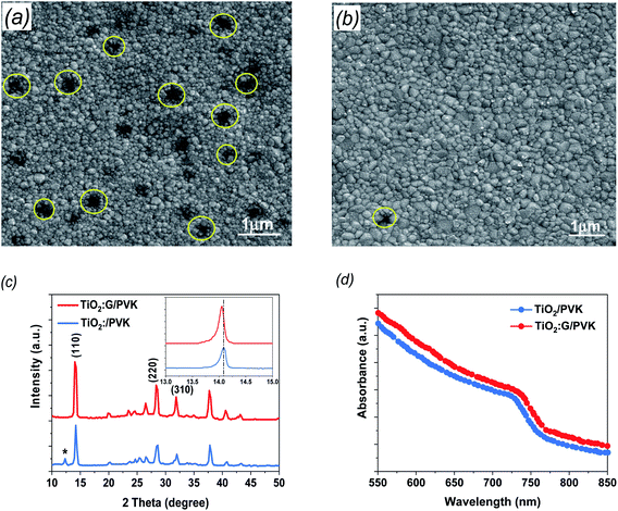
To gain further information about the prepared G:TiO2 applied in the device structure, different characterization techniques were utilized. The surface morphologies of the perovskite layer on bare TiO2 as well as on G:TiO2 films were checked via FESEM analysis and are illustrated in Fig. 3 (a and b), respectively. The SEM image of perovskite over 0.0% G:TiO2 film displays different pinholes and drops in the covering process (Fig. 3a), while after adding graphene to the composition of the TiO2, the surface coverage as well as the crystallinity of the deposited perovskite film were enhanced due to the higher conductivity gained from the existence of graphene materials (Fig. 3b). The results obtained from the SEM image of perovskite over the 1.5% G:TiO2 film confirm the importance of graphene doping inside the ETL to gain a uniform layer with no major alterations in the surface morphology. Besides, the perovskite layer deposited on the 1.5% G:TiO2 film has a greater average grain size than that on the 0.0% G/TiO2 film, elucidating the higher value of Voc and a lower hysteresis in 1.5% G:TiO2 PSCs. Furthermore, the XRD patterns of the resulting perovskite films (Fig. 3c) yielded identical crystal structures with (110), (220), and (310) diffraction peaks at 14.07°, 28.3°, and 31.7°. The peak at 14.07° in the 0.0% G:TiO2/perovskite film corresponds to the PbI2 phase correlated with the decomposition of a small amount of perovskite during thermal annealing.36 On the other hand, no peak of PbI2 could be detected in the XRD of the 1.5% G:TiO2/perovskite film. Also, the peak intensities of the 1.5% G:TiO2/perovskite film designate a considerable development compared to those of the 0.0% G:TiO2/perovskite film, especially for the (110) peak, indicating that the addition of graphene could augment the crystallinity of mixed perovskite.37
To elucidate the optical properties of the deposited perovskite layer over TiO2 and TiO2 containing 1.5% graphene as an ETL, we checked these data via UV-visible spectrophotometry (Fig. 3d). The absorbance of both samples established a comparable spectrum in the visible region with an onset at 780 nm, which slightly increased after the addition of 1.5% graphene doping and is consistent with a previous report.38 In addition, the acquired results display that the perovskite films deposited over TiO2 containing 1.5% graphene can harvest more light, which should be satisfactory to advancing the performance of the fabricated PSCs.
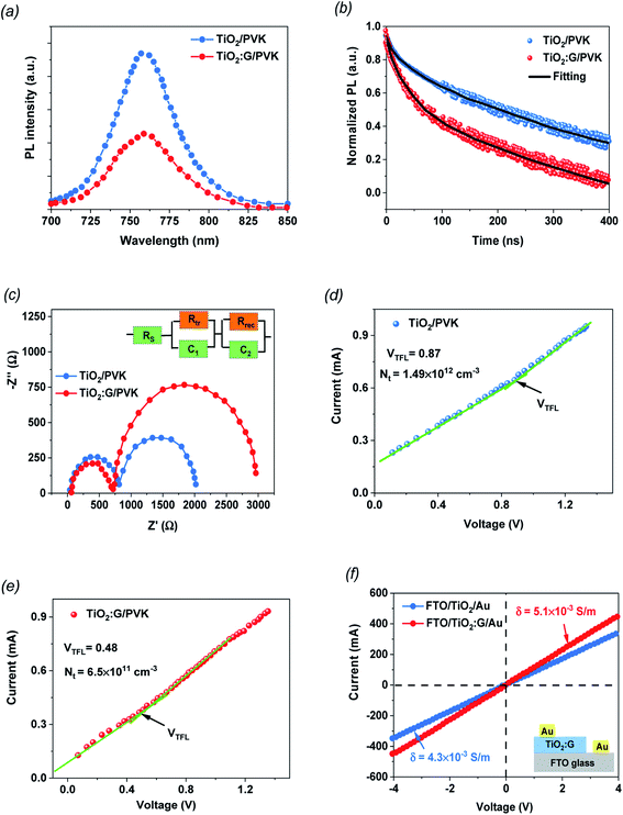
PL spectroscopy was used to check the charge-extraction properties of the fabricated PSC devices based on PVK deposited on TiO2 and TiO2 containing 1.5% graphene as the ETL films. The steady-state PL (Fig. 4a) was measured for both samples to evaluate the influence of PL quenching of the PVK. The perovskite layer on the 1.5% G:TiO2 film displays a noteworthy PL-quenching effect that confirms the improved behavior in charge collection because of the lower surface defects at the interface, supported by the graphene doping. TRPL analysis was established to further investigate the photo-induced charges dynamics, including charge extraction and recombination. Fig. 4b demonstrates the PL transient profiles of PVK deposited on TiO2 and TiO2 containing 1.5% graphene as the ETL films and displays the average recombination lifetime (τave) that can be checked via a three-component exponential decay function.42 The fitted time coefficients (τ1, τ2 and τ3) with the corresponding relative amplitudes (A1, A2 and A3) based on the three-component exponential decay function for TRPL spectra of the PSCs with and without graphene are summarized on Table 2. The optimized PSC with TiO2 containing 1.5% graphene shows a significant drop in the PL decay time data compared with that of the control PSC based on TiO2 without graphene doping. Besides, the τave is reduced from 137.32 ns to 105.43 ns after graphene incorporation, setting an improved electron injection from the PVK layer into the TiO2 containing 1.5% graphene. Furthermore, the Nyquist measurements were checked by EIS studies for the fabricated PSC devices based on PVK deposited on TiO2 and TiO2 containing 1.5% graphene as the ETL films to additionally recognize to the role of the graphene additive (Fig. 4c). It is clear that the arc of the PSC with the TiO2 containing 1.5% graphene film is smaller than that of PSC based on the pure TiO2 film, indicating that the hybrid photoelectrode of graphene and TiO2 suppresses the charge-transport resistance (Rtr). Nyquist plots show charge-transfer resistances of 812 Ω and 718 Ω for the devices based TiO2 and TiO2 containing 1.5% graphene as an ETL, respectively, with corresponding recombination resistances of 2018 and 2962 Ω for both devices, respectively. It is evident that the cell with a photoelectrode doped with graphene exposes a smaller charge-transport resistance and higher recombination resistances, signifying a fast charge transfer ability and a lower recombination rate compared to those of the control cell, as evidenced by the higher Jsc values.39,40 Additionally, the inset in Fig. 4c discusses the equivalent circuits of the PSCs. Furthermore, the space-charge-limited current (SCLC) model was used to recognize the mechanism of conductivity enhancement for TiO2 and G:TiO2 ETLs with an electron only cell architecture, and the obtained J–V plots are described in Fig. 4(d and e). Besides, the I–V curves are linear in the low voltage region and then the current discloses a sharp increment after a certain voltage i.e., trap-filled limit voltages (VTFL) because the trap states have been filled. Correspondingly, the VTFL values of the pure TiO2 film and the G:TiO2 films are 0.87 and 0.48 V, respectively. The trap-state density (ntrap) of G:TiO2 (6.50 × 1011 cm−3) is lower than that of pure TiO2 (1.49 × 1012 cm−3). Such a higher electron mobility and lower trap density of the G:TiO2 film is favorable for an efficient forward electron flow and as a consequence the photovoltaic performance of the perovskite solar cells has been developed.
| Type | A 1 | τ 1 (ns) | A 2 | τ 2 (ns) | A 3 | τ 3 (ns) | τ ave (ns) |
|---|---|---|---|---|---|---|---|
| TiO2/PVK | 0.38 | 6.67 | 0.32 | 28.32 | 0.48 | 155.03 | 137.32 |
| G:TiO2/PVK | 0.52 | 5.92 | 0.42 | 22.45 | 0.21 | 141.89 | 105.43 |
Moreover, the I–V measurements were checked through the sandwich structures of FTO/TiO2/Au and FTO/G:TiO2/Au to examine the change in electrical properties of the TiO2 ETL through the addition of graphene materials. The bias potential between the FTO and Au electrodes continuously increased from −1 V to 1 V and the thicknesses of the ETL are the same in the cases of TiO2 and G:TiO2. The current–voltage (I–V) plots recorded in the dark for various ETLs are demonstrated in Fig. 4f. The augmentation in the current was detected for the G:TiO2 ETL. The acquired curves illustrate that the conductivity (σ) of the different ETLs was found to be 4.30 × 10⁻⁵ and 5.10 × 10⁻⁵ S m−1 for FTO/TiO2/Au and FTO/G:TiO2/Au, respectively, showing a higher conductivity for G:TiO2 samples compared to that of the bare TiO2.41
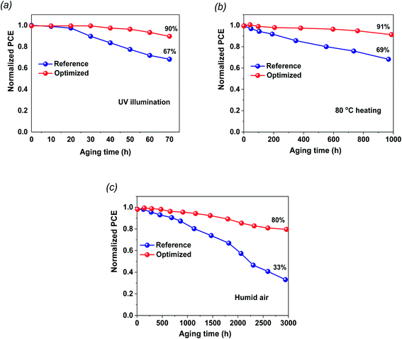
The stability of the fabricated cells in ambient conditions and during thermal annealing is a fundamental challenge for dedicated commercialization. The shelf-life stabilities of the FTO/TiO2/PVK/Au and FTO/G:TiO2/PVK/Au devices were checked without any encapsulation (Fig. 5). The stability test results of the perovskite devices based on TiO2 and on G:TiO2 ETLs under continuous UV light illumination at room temperature are found in Fig. 5a. The devices that contain graphene doped TiO2 and bare TiO2 as the ETLs retained 90 and 87%, respectively, of the initial efficiency results. Besides, the 1.5% G:TiO2 device retained 80% of its initial PCE, which designates a superior reliability comparative to that of the 0.0% G:TiO2 device (∼33% of its initial PCE). Additionally, PCE of the unencapsulated device retained more than 91% after thermal annealing at 80 °C for 1000 h under ambient conditions, demonstrating the superior thermal stability of the 1.5% G:TiO2 doped device compared to that of the bare TiO2 device (Fig. 5b). The devices were stored in wet conditions (∼30% RH) and the PV characteristics were measured over 3000 h (Fig. 5c). The improved stability of the 1.5% G:TiO2 device could be accredited to improved features of the ETL and lower trap states in the graphene-doped TiO2. The devices based on the G:TiO2 ETL display an outstanding performance and sensible stability that propose the awesome candidacy of G:TiO2 ETL for utilization in perovskite solar cells.
4. Conclusion
In summary, graphene material was doped into TiO2 with different molar ratios to obtain reliable ETLs for fabricating high-performance and long-term stable HTL-free PSCs. The best efficiency of 16.75% was achieved with a lower hysteresis effect by using 1.5% G:TiO2 as the ETL. Graphene materials contribute to a better interfacial contact between the TiO2 ETL and perovskite and permit perovskite to grow with bigger grains and a pinhole-free surface. Several techniques, including XRD, absorbance, FESEM, PL and cell parameters, were applied to give detailed studies and characterize the fabricated materials and devices. Additionally, the fabricated PSCs based on G:TiO2 ETL indicate a long-term stability in the ambient environment compared to that of the pristine devices. The current study supports that including graphene in the TiO2 structure is a feasible method to achieve high-quality mixed cation perovskite solar cells in ambient air for outstanding HTL-free PSCs.Conflicts of interest
The authors declare that they have no conflicts of interest.Acknowledgements
AES is currently on leave from CMRDI. The authors of the article would like to show their appreciation to the Middle Technical University, Baghdad in Iraq for the financial support. Furthermore, AES is grateful for the National Research grants from MINECO, Spain, “Juan de la Cierva” [FJCI-2018-037717].References
- H. Wang, F. Yang, N. Li, J. Song, J. Qu, S. Hayase and W.-Y. Wong, Chem. Eng. J., 2020, 392, 123677 CrossRef CAS.
- Y. Shi, W. Chen, Z. Wu, Y. Wang, W. Sun, K. Yang, Y. Tang, H. Y. Woo, M. Zhou, A. B. Djurišić, Z. He and X. Guo, J. Mater. Chem. A, 2020, 8, 13754–13762 RSC.
- H. Wang, F. Yang, Y. Xiang, S. Ye, X. Peng, J. Song, J. Qu and W.-Y. Wong, J. Mater. Chem. A, 2019, 7, 24191–24198 RSC.
- A. E. Shalan, T. Oshikiri, H. Sawayanagi, K. Nakamura, K. Ueno, Q. Sun, H.-P. Wu, E. W.-G. Diau and H. Misawa, Nanoscale, 2017, 9, 1229–1236 RSC.
- A. M. Elseman, S. Sajid, A. E. Shalan, S. A. Mohamed and M. M. Rashad, Appl. Phys. A: Mater. Sci. Process., 2019, 125, 476 CrossRef.
- C. Zhang, S. Wang, H. Zhang, Y. Feng, W. Tian, Y. Yan, J. Bian, Y. Wang, S. Jin, S. M. Zakeeruddin, M. Grätzelb and Y. Shi, Energy Environ. Sci., 2019, 12, 3585–3594 RSC.
- A. E. Shalan, A. N. El-Shazly, M. M. Rashad and N. K. Allam, Nanoscale Adv., 2019, 1, 2654–2662 RSC.
- A. E. Shalan, Mater. Adv., 2020, 1, 292 RSC.
- A. E. Shalan, S. Kazim and S. Ahmad, ChemSusChem, 2019, 12, 4116–4139 CrossRef CAS.
- K. A. M. Mustafa, K. A. Ali, S. M. Mohammed and M. A. Abdulnasser, Chem. Phys. Lett., 2020, 754, 137718 CrossRef.
- A. E. Shalan, W. Sharmoukh, A. N. Elshazly, M. M. Elnagar, S. A. Al Kiey, M. M. Rashad and N. K. Allam, Sustainable Mater. Technol., 2020, 26, e00226 CrossRef.
- M. K. A. Mohammed, RSC Adv., 2020, 10, 35831 RSC.
- K. A. Ali and K. A. M. Mustafa, J. Sol-Gel Sci. Technol., 2020, 96, 659–668 CrossRef.
- M. K. A. Mohammed, Ceram. Int., 2020, 46, 27647–27654 CrossRef CAS.
- S. A. Duha and K. A. M. Mustafa, Sol. Energy, 2020, 207, 1240–1246 CrossRef.
- Z. Ku, Y. Rong, M. Xu, T. Liu and H. Han, Sci. Rep., 2013, 3, 3132 CrossRef.
- A. E. Shalan, A. M. Elseman, M. Rasly, M. M. Moharam, M. Lira-Cantu and M. M. Rashad, RSC Adv., 2015, 5, 103095–103104 RSC.
- A. E. Shalan, M. M. Rashad, Y. Yu, M. Lira-Cantú and M. S. A. Abdel-Mottaleb, Electrochim. Acta, 2013, 89, 469–478 CrossRef CAS.
- M. M. Rashad and A. E. Shalan, Appl. Phys. A: Mater. Sci. Process., 2014, 116, 781–788 CrossRef CAS.
- M. K. A. Mohammed, Optik, 2020, 217, 164867 CrossRef CAS.
- J. Zhou, Z. Ye, J. Hou, J. Wu, Y. Z. Zheng and X. Tao, J. Mater. Chem. A, 2018, 6, 22626–22635 RSC.
- T. H. Schloemer, J. A. Christians, J. M. Luther and A. Sellinger, Chem. Sci., 2019, 10, 1904–1935 RSC.
- L. Jiang, J. Lu, S. R. Raga, J. Sun, X. Lin, W. Huang, F. Huang, U. Bach and Y. B. Cheng, Nano Energy, 2019, 58, 687–694 CrossRef CAS.
- A. M. Elseman, A. H. Zaki, A. E. Shalan, M. M. Rashad and Q. Song, Ind. Eng. Chem. Res., 2020, 59(41), 18549–18557 CrossRef CAS.
- B. Munkhbayar, J. M. Thomas, J. S. Cameron, B.-E. Munkhjargal, W. Yun, J. B. Mark, P. P. Ivan, N. Thomas and G. S. Joseph, Adv. Sci., 2017, 1600504 Search PubMed.
- S. R. B. Abdulaziz, Y. LePing, A. T. Sherif, J. S. S. Michelle, E. S. Paul, B. Munkhbayar and G. S. Joseph, iScience, 2019, 14, 100–112 CrossRef.
- S. H. Gill, H. S. Young, U. J. Young, L. Jin-Wook, P. Nam-Gyu, K. K. Bong, L. Jung-Kun, S. C. In, H. Y. Dae and S. J. Hyun, ACS Appl. Mater. Interfaces, 2015, 7, 23521–23526 CrossRef.
- T.-W. W. Jacob, M. B. James, M. B. Eva, A. Antonio, A. A.-W. Jack, H. Jian, S. Michael, M.-S. Ivan, B. Juan, J. S. Henry and J. N. Robin, Nano Lett., 2014, 14, 724–730 CrossRef.
- Z. Jianjun, T. Tong, Z. Liuyang, L. Xiaohe, Z. Haiyuan and Y. Jiaguo, ACS Sustainable Chem. Eng., 2018, 6, 8631–8640 CrossRef.
- T. Huijie, C. Qi, Z. He, W. Shuangjie, H. Jian, L. Tongtong, G. Bingyu, Y. Jiabao, D. Dongshan and L. Xuanhua, Sol. RRL, 2020, 4, 1900415 CrossRef.
- P. Shangzheng, Z. Chunfu, Z. Hairong, D. Hang, C. Dazheng, Z. Weidong, X. He, C. Jingjing, L. Zhenhua, Z. Jincheng and H. Yue, Appl. Surf. Sci., 2020, 507, 145099 CrossRef.
- S. Deli, Z. Weifeng, X. Fengyan, L. Yafeng, A. Antonio and W. Mingdeng, J. Power Sources, 2018, 402, 320–326 CrossRef.
- Z. Zonglong, M. Jiani, W. Zilong, M. Cheng, F. Zetan, D. Lili, B. Yang, F. Louzhen, Y. He, L. P. David and Y. Shihe, J. Am. Chem. Soc., 2014, 136, 3760–3763 CrossRef.
- A. E. Shalan, S. Narra, T. Oshikiri, K. Ueno, X. Shi, H.-P. Wu, M. M. Elshanawany, E. W.-G. Diau and H. Misawa, Sustainable Energy Fuels, 2017, 1, 1533–1540 RSC.
- D. Zhang, X. Zhang, S. Bai, C. Liu, Z. Li, W. Guo and F. Gao, Sol. RRL, 2019, 1900154 CrossRef.
- D. S. Ahmed, M. K. A. Mohammed and M. R. Mohammad, Chem. Pap., 2020, 74, 197–208 CrossRef CAS.
- S. Siraj, Ve. Jayaramakrishnan, D. Elder, A. P.-G. Sergio, R.-O. Gabriel and L.-L. Tzarara, Carbon, 2019, 146, 388–398 CrossRef.
- R. M. Mohammad, D. S. Ahmed and K. A. M. Mustafa, J. Sol-Gel Sci. Technol., 2019, 90, 498–509 CrossRef.
- B. Munkhbayar, J. M. Thomas, J. S. Cameron, B.-E. Munkhjargal, W. Yun, J. B. Mark, P. P. Ivan, N. Thomas and G. S. Joseph, Mater. Adv., 2017, 1600504 Search PubMed.
- S. H. Gill, H. S. Young, U. J. Young, L. Jin-Wook, P. Nam-Gyu, K. K. Bong, L. Jung-Kun, S. C. In, H. Y. Dae and S. J. Hyun, ACS Appl. Mater. Interfaces, 2015, 7, 23521–23526 CrossRef.
- R. M. Mohammad, S. A. Duha and K. A. M. Mustafa, Surf. Rev. Lett., 2020, 27, 1950123 CrossRef.
- K. A. M. Mustafa, G. Sarusi, P. Sakthivel, G. Ravi and U. Y., Mater. Res. Bull., 2021, 137, 111182 CrossRef.
| This journal is © The Royal Society of Chemistry 2021 |

