
 Open Access Article
 This Open Access Article is licensed under a
 Creative Commons Attribution 3.0 Unported Licence
Production of mixed phase Ti3+-rich TiO2 thin films by oxide defect engineered crystallization†
Lauri
Palmolahti
 a,
Harri
Ali-Löytty
*ab,
Markku
Hannula
a,
Tuomas
Tinus
a,
Kalle
Lehtola
a,
Antti
Tukiainen
c,
Jarno
Reuna
c and
Mika
Valden
*a
a,
Harri
Ali-Löytty
*ab,
Markku
Hannula
a,
Tuomas
Tinus
a,
Kalle
Lehtola
a,
Antti
Tukiainen
c,
Jarno
Reuna
c and
Mika
Valden
*a
aSurface Science Laboratory, Physics Unit, Faculty of Engineering and Natural Sciences, Tampere University, Tampere, Finland. E-mail: harri.ali-loytty@tuni.fi; mika.valden@tuni.fi
bLiquid Sun Ltd, Tampere, Finland
cFaculty of Engineering and Natural Sciences, Tampere University, Tampere, Finland
First published on 7th November 2024
Abstract
Amorphous TiO2 has insufficient chemical stability that can be enhanced with annealing induced crystallization. However, the crystalline structure is already predetermined by the defect composition of the amorphous phase. In this paper, we demonstrate that the oxide defects, i.e., oxygen vacancies and Ti3+ states, can be created by O2 deficiency during ion-beam sputter deposition without affecting the O/Ti ratio of TiO2. The films are thus stoichiometric containing a variable degree of interstitial O instead of lattice O. Defect-free TiO2 crystallizes into microcrystalline anatase during vacuum annealing, whereas a moderate number density of defects causes crystallization into nanocrystalline rutile. An excessive number density of defects results in a mixed amorphous/nanocrystalline rutile phase that was analyzed by near-edge X-ray absorption fine structure (NEXAFS) spectroscopy. The number density of defects did not affect the crystallization temperature, which was 400 °C. All crystalline films, including the mixed amorphous/nanocrystalline rutile phase, were chemically stable in 1.0 M NaOH for 80 h. Unlike annealing treatments in oxidizing environments that are typically applied to improve stability, vacuum annealing improves the stability preserving also the Ti3+ gap states that are critical to the charge transfer in protective TiO2-based photoelectrode coatings.
1 Introduction
The modification of the crystal structure and defect composition of TiO2 thin films has gained a lot of interest as they significantly impact the chemical stability, optical absorption, and charge transfer properties of TiO2.1–5 Anatase and rutile are the two main polymorphs of TiO2, with rutile being thermodynamically the most stable one.6 The crystallization of TiO2 is strongly affected by the presence of oxygen vacancies (Ov)1,2,6 and it has been suggested that the Ov in amorphous TiO2 predetermine to which crystalline phase TiO2 crystallizes upon annealing.2 Besides pure phases, mixed phases have gained interest due to their improved photocatalytic properties.7 Visible light sensitive black TiO2 photocatalysts can be fabricated by thermal treatments under non-oxidative conditions.5 Kang et al. have suggested that an excessive number density of Ov causes amorphous TiO2 to crystallize into a mixed amorphous–crystalline phase.1The formation of an Ov forces three adjacent hexa-coordinated Ti4+ atoms to change into penta-coordinated Ti atoms, two of which change their valence state from 4+ to 3+.8–10 Thus the Ov defects promote the formation of Ti3+ defects. These oxygen defects act as crystallization centers affecting the crystallization of amorphous TiO2 during annealing.11 The higher the concentration of crystallization centers, the closer the growing crystal grains are to each other. Therefore, increasing the number density of Ov and Ti3+ defects is expected to decrease the resulting crystallite size in annealing induced crystallization. The Ov also decrease the energy required to rearrange the atoms.12 Because rutile has a lower Gibbs free energy than anatase, making it the most stable polymorph,6 and because a high Ov concentration has been shown to promote crystallization to rutile through lattice relaxation,6,13 it is expected that defect-rich amorphous TiO2 will crystallize into rutile. Annealing in an oxygen-free environment, e.g., in an ultra-high vacuum, does not oxidize the Ti3+ defects, thus preserving the exceptional charge transfer properties of Ti3+-rich TiO2.
Ov can be created by doping or annealing in a reductive environment, or with sputtering induced defects.14 More importantly, Ov are formed if the deposition of TiO2 is performed under O deficient conditions.2 Amorphous TiO2 can be deposited using various methods including atomic layer deposition (ALD), pulsed laser deposition, and ion-beam sputtering (IBS), in which the number density of Ov or Ti3+ defects can be adjusted by controlling the deposition temperature or the amount of O2 present during the deposition.2,4 O deficiency in amorphous TiO2 has been shown to affect polymorph selection during annealing induced crystallization.15–17 Ov and Ti3+ defects can be created without changing the stoichiometry of TiO2 and an increase in the defect concentration does not necessarily indicate that O atoms are removed from TiO2. Interstitial peroxo species can be formed with the formation of Ov and Ti3+ defects, thus resulting in defect-rich but stoichiometric TiO2.4,8
One potential use of TiO2 thin films is protective coatings used in artificial photosynthesis to protect the photocatalytic material.18,19 The phase structure and defect composition of TiO2 have been shown to have a significant effect on the chemical stability of TiO2.4 Thus, control of the phase composition of TiO2via oxide defect engineering can be used to enhance the chemical stability.
In our earlier research,4 we have shown that the crystallization of amorphous ALD grown TiO2 during vacuum annealing depends strongly on the amount of tetrakis(dimethylamino)titanium (TDMAT) precursor fragments and Ti3+ defects in the TiO2 film. The decreased amount of precursor fragments and increased number density of Ti3+ defects changed the resulting crystal structure from anatase to rutile and decreased the crystallization onset temperature. However, because both the amount of precursor fragments and Ti3+ defects depend on the deposition temperature, it was not possible to differentiate their roles in crystallization.
In this research, the effect of Ov and Ti3+ defects on vacuum annealing induced crystallization of IBS deposited amorphous stoichiometric TiO2 thin films was investigated. In contrast to ALD, IBS deposition serves as a method for growing TiO2 thin films with a controlled number density of Ti3+ defects but without precursor fragments. The number density of defects (Ti3+/Ti = 0.1–10.5%) in the as deposited samples was controlled by altering the O2 background flow during the deposition to create an O deficient growth environment. The samples were annealed in an ultra-high vacuum (200–500 °C) and the chemical composition, crystal structure, and defect concentrations were analyzed after each annealing step with photoelectron spectroscopy and near edge X-ray absorption fine structure (NEXAFS) spectroscopy. The O2 deficiency during the deposition created Ti3+ and Ov defects, but surprisingly did not affect the O/Ti ratio of TiO2. A low concentration of Ti3+ defects (0.1%) resulted in microcrystalline anatase after vacuum annealing, whereas a medium concentration (6.4%) resulted in nanocrystalline rutile and a high concentration (10.5%) resulted in a mixed nanorutile–amorphous phase.
2 Experimental
2.1 Sample preparation and characterization
TiO2 thin films were fabricated using IBS on a prepolished p-type Si(100) wafer (Siegert Wafer, B doped). Sputtering was carried out in a Navigator 700 (Cutting Edge Coatings GmbH) reactive ion beam sputtering system. Sputtering was performed using an ion beam of an Ar![[thin space (1/6-em)]](https://www.rsc.org/images/entities/char_2009.gif) :O2 mixture with flow rates of 8 sccm and 0.5 sccm, respectively. The number density of Ti3+ defects was controlled by the oxygen deficiency (O2 background flow) during the deposition. The background O2 flow that is aimed directly at the sputtering target was varied for each growth using 40, 20, and 10 sccm flow rates and the samples are labeled accordingly as TiO2-40, TiO2-20, and TiO2-10. A 200 mm × 200 mm titanium plate with a purity of 99.8% was used as the sputtering target. The main sputtering parameters, namely the ion source radiofrequency power, the ion beam current, and the ion beam voltage, were kept constant at 150 W, 230 mA, and 2 kV, respectively. The film thickness was controlled with a deposition time that was 353 s for the TiO2-40 and TiO2-20 samples. The deposition time was 217 s for the TiO2-10 samples to compensate for the faster growth rate due to the lower O2 background pressure. Similar sets of TiO2 thin films were deposited on quartz glass substrates for optical measurements.
:O2 mixture with flow rates of 8 sccm and 0.5 sccm, respectively. The number density of Ti3+ defects was controlled by the oxygen deficiency (O2 background flow) during the deposition. The background O2 flow that is aimed directly at the sputtering target was varied for each growth using 40, 20, and 10 sccm flow rates and the samples are labeled accordingly as TiO2-40, TiO2-20, and TiO2-10. A 200 mm × 200 mm titanium plate with a purity of 99.8% was used as the sputtering target. The main sputtering parameters, namely the ion source radiofrequency power, the ion beam current, and the ion beam voltage, were kept constant at 150 W, 230 mA, and 2 kV, respectively. The film thickness was controlled with a deposition time that was 353 s for the TiO2-40 and TiO2-20 samples. The deposition time was 217 s for the TiO2-10 samples to compensate for the faster growth rate due to the lower O2 background pressure. Similar sets of TiO2 thin films were deposited on quartz glass substrates for optical measurements.
The as deposited samples and vacuum annealed samples were characterized using UV–vis spectroscopy (Lambda 1050 UV/VIS/NIR spectrometer, PerkinElmer), scanning electron microscopy (SEM, Zeiss Ultra-55), grazing incidence X-ray diffraction (GIXRD) and X-ray reflectivity (XRR, PANalytical X'Pert3 MRD diffractometer). SEM images were taken using an in-lens detector at an acceleration voltage of 1 kV. GIXRD was performed using Cu Kα radiation at a cathode voltage of 45 kV and a cathode current of 40 mA. A 0.02 mm thick nickel beta filter with an attenuation factor of 2.5 was used to attenuate the Cu Kβ peak. XRR was measured in the coupled ω–2θ mode. XRR spectra were analyzed using the GenX program (version 3.5.5).20 In the analysis, a TiO2–SiO2–Si structure was modeled to match the measured reflectance spectra and the densities and thicknesses of the layers and surface roughness were obtained from the fitting parameters. UV–vis transmittance and reflectance spectra were recorded using an integrating sphere module (150 mm InGaAs Int. Sphere).
2.2 X-ray photoelectron spectroscopy
The samples were loaded into NanoESCA photoelectron spectroscopy system (Omicron NanoTechnology GmbH), and X-ray photoelectron spectroscopy (XPS) measurements were performed using a monochromatized Al Kα (hν = 1486.6 eV) excitation source. The samples were cumulatively annealed at 300 and 500 °C in NanoESCA in an ultra-high vacuum using radiative heating. The dwell time was 15 minutes, and the temperature was measured with a Land Cyclops 160B pyrometer using an emissivity of 0.60. XPS spectra were recorded before annealing and after both annealing steps. XPS data were fitted with Gaussian/Lorentzian components and Shirley type background subtraction using CasaXPS version 2.3.25PR1.0. The O/Ti ratio was calculated from the peak areas using experimental sensitivity factors determined from a rutile reference sample.2.3 Near edge X-ray absorption fine structure spectroscopy
A set of as deposited TiO2 thin films was transferred to the solid-state end station (SSES) of the FinEstBeAMS beamline at MAX IV Laboratory, Lund, Sweden, where NEXAFS spectroscopy was performed.21 The samples were cumulatively annealed in the preparation chamber of SSES from 200 °C to 500 °C in 50 °C steps. The temperature ramp time and dwell time were both 15 minutes. Annealing was done in an ultra-high vacuum (p < 5 × 10⁻⁸ mbar) using electron beam bombardment and the temperature was measured with a Land Cyclops 160B pyrometer using an emissivity of 0.60. NEXAFS spectroscopy was performed at room temperature in the analysis chamber of SSES before annealing and after each annealing step.Both the bulk sensitive total yield and surface sensitive Auger yield NEXAFS spectra were recorded simultaneously. The total yield spectra were recorded from the drain current of the sample and the Auger yield NEXAFS spectra from the middle of the corresponding Auger electron peak with a dwell time of 1 s. The kinetic energy window was 510.8–516.2 eV for the O K-edge. In both modes, the photon beam induced current was measured from a gold grid that was positioned in the path of the photon beam. The measured absorption was normalized by this current, as it is proportional to the photon flux. NEXAFS spectra were normalized so that the background level before the absorption edge was set to zero and the edge jump was normalized to one. The reference spectra of anatase, rutile, and amorphous phases were fitted to the data using the least squares method.
2.4 Electrochemical impedance spectroscopy
Electrochemical impedance spectroscopy (EIS) was performed using the as deposited and vacuum annealed TiO2/Si samples in 1.0 M NaOH (Sigma-Aldrich, sodium hydroxide, reagent grade). The measurements were done in a custom-made electrochemical cell using a three electrode setup with platinum wire as a counter electrode and the leak-free reference electrode 69-0023 (Harvard Apparatus) as a reference electrode. The sample was used as the working electrode and the area in contact with the electrolyte was sealed using an O-ring with a diameter of 6 mm. The total volume of the cell was 3.5 ml. The measurement was done using an Autolab PGSTAT12 (Metrohm AG) potentiostat/galvanostat in the galvanostatic mode at 0 A. The impedance was measured from 1 MHz to 0.01 Hz using an amplitude of 10 μA. The measurements were repeated every 15 min for 80 h to test the chemical stability of the samples.3 Results
3.1 Structural analysis
The effect of the O2 background flow during the deposition on the structure of the as deposited samples and the samples vacuum annealed at 500 °C was characterized by GIXRD and SEM (Fig. 1). None of the as deposited samples showed any peaks in the GIXRD patterns or any structure in the SEM images, which indicates an amorphous phase.23 After annealing in a vacuum at 500 °C, the TiO2-40 sample exhibited clear anatase (101) and (200) peaks and the TiO2-20 sample exhibited a wide rutile (110) peak whereas the TiO2-10 sample did not exhibit any peaks.22 The FWHM of the rutile (110) peak is 3.0° which roughly corresponds to a crystallite size of 3 nm, whereas the anatase 101 peak has a FWHM of 0.7° which corresponds to a crystallite size of 12 nm.24 The measured GIXRD peak ratios are not the same as that for the powder references due to anisotropy. The SEM images show that all the annealed samples have a clear grain structure. The TiO2-40 sample exhibits very large (>1 μm) elongated grains whereas the TiO2-20 and TiO2-10 samples exhibit nano-scale grains (<100 nm) without directional texture. From these results, it can be concluded that the TiO2-40 sample crystallizes into micro-crystalline anatase and the TiO2-20 sample into nano-crystalline rutile during vacuum annealing. A large area SEM image of the TiO2-40 sample after annealing is presented in Fig. S1† and shows grain lengths up to 10 μm. | ||
| Fig. 1 (a) GIXRD patterns of the as deposited samples and the samples vacuum annealed at 500 °C. Anatase and rutile reference peak positions22 are shown on top and the height of the reference lines indicates the relative intensity of the reference peaks for powder samples. (b) SEM images of the as deposited samples and the samples vacuum annealed at 500 °C. | ||
The results obtained from the vacuum annealed TiO2-10 sample are particularly interesting because the SEM images indicated a nano-scale structure, but no GIXRD peaks were observed. This may be due to the nano-scale grain size, as it can result in such wide and low GIXRD peaks that they become indistinguishable. The structure of the annealed TiO2-10 sample was further analyzed by NEXAFS spectroscopy, as it is more sensitive to the nearest neighbor structure.
The thickness and density of the TiO2 films were determined from the XRR patterns by fitting the measured pattern with modeled patterns of the TiO2–SiO2–Si layer structure. The thicknesses of the as deposited TiO2-40, TiO2-20, and TiO2-10 samples were 34.0, 43.2, and 37.8 nm, respectively. After annealing at 500 °C, the thicknesses were slightly smaller: 33.1, 40.6 and 36.5 nm. Based on our test on a thicker sample (60.7 nm), the film thickness had no significant effect on the crystallization or defect formation. As the annealing is done in a vacuum, the ambient O2 partial pressure does not affect the crystallization. The presence of O2 could cause film thickness related differences in the crystallization because in a thicker film, a smaller proportion of Ti atoms could react with O2. The densities of the samples are presented in Table 1. The density of TiO2 increased slightly with increasing oxygen deficiency during the IBS fabrication process as the Ov made the TiO2 denser by shortening the remaining Ti–O bond lengths.10,25 After annealing at 500 °C, the TiO2-20 and TiO2-10 samples had higher densities of 4.00 and 4.01 g cm−3, respectively, whereas the TiO2-40 sample had a density of 3.68 g cm−3. Rutile is denser than anatase6 and thus the measured densities suggest that rutile is a possible phase for the TiO2-20 and TiO2-10 samples after annealing. For the TiO2-20 sample, this is also supported by the GIXRD and SEM results.
| TiO2-40 | TiO2-20 | TiO2-10 | |
|---|---|---|---|
| As deposited | |||
| Density (g cm−3) | 3.66 | 3.78 | 3.86 |
| α @ 528 nm (103 cm−1) | 8.4 | 22.9 | 70.9 |
| O/Ti | 2.04 | 2.03 | 2.04 |
| Ti3+/Ti (%) | 0.1 | 6.4 | 10.5 |
| O1−/O (%) | 3.9 | 5.0 | 6.1 |
| Ti3+ 3dxy/VB (%) | 0 | 0 | 1.4 |
| Annealed at 500 °C | |||
| Density (g cm−3) | 3.68 | 4.00 | 4.01 |
| α @ 528 nm (103 cm−1) | 47.8 | 35.6 | 69.2 |
| O/Ti | 2.00 | 2.04 | 2.10 |
| Ti3+/Ti (%) | 3.7 | 19.4 | 41.3 |
| O1−/O (%) | 12.6 | 12.7 | 19.1 |
| Ti3+ 3dxy/VB (%) | 0 | 1.7 | 3.9 |
3.2 Chemical composition and defect concentrations
The chemical composition and defect concentrations of the as deposited samples and samples vacuum annealed at 500 °C were characterized using XPS (Fig. 2). Four elements, O, Ti, C (<7%), and Ar (<0.8%), were detected from the survey spectra (Fig. S2†). C is an impurity from the atmosphere that is on top of the sample and Ar is from the fabrication process as it is used as a sputtering gas in IBS. The amount of C and Ar did not have significant differences between the samples, and C was removed during the annealing series. | ||
| Fig. 2 XP spectra of O 1s, Ti 2p and valence band of the as deposited samples and the samples vacuum annealed at 500 °C. The spectra were recorded using Al Kα radiation (hν = 1486.6 eV). The intensities are normalized so that each spectrum has the same area. | ||
Three chemical states were identified from both O 1s and Ti 2p spectra.4,8,26 The O2− and Ti4+ components can be assigned to TiO2, whereas the O1− and Ti3+ components are related to the Ov and Ti3+ defects. The third components are peroxo and Ti2+ species, but the amount of these species is small.8 The in-gap Ti3+ 3dxy state was identified just below the Fermi level in the valence band spectra.
The Ti3+/Ti, O/Ti, O1−/O, and Ti3+ 3dxy/VB ratios are presented in Table 1 for the as deposited samples and for the samples vacuum annealed at 500 °C. The as deposited TiO2-40 sample had a negligible number density of Ti3+ defects whereas TiO2-20 had 6.4% and the TiO2-10 sample had 10.5%. The number density of Ti3+ defects increased during the annealing. The samples that already had a large number density of Ti3+ defects also had the largest increase in it during the annealing. The increase in the defect density is linked to the thermal rearrangement during the crystallization.4 The crystallization can cause the formation of interfacial defects at the grain boundaries. Materials with smaller crystallite sizes have larger total grain boundary areas, explaining why the samples with the smallest crystallite sizes had the largest increase in the defect density during the crystallization. Unexpectedly, the O/Ti ratio was the same for all as deposited samples regardless of the oxygen deficiency during the deposition and the ratio is close to the stoichiometric value of 2 despite the strong difference in the number density of Ti3+ defects. Vacuum annealing had a negligible effect on the O/Ti ratio, which indicates that O is not removed from the samples during vacuum annealing. Thus, there is no formation of Ti suboxides, e.g., Ti2O3, during annealing. This is contradictory to some earlier research where the formation of Ti3+ defects is linked to the O deficiency in TiO2.27,28 The information depth of the XPS measurements was about 6 nm, which represents a significant proportion of the film thickness.
The O1−/O ratio increases with the number density of Ti3+ defects, as the charge neutrality principle suggests that an equal number density of O1− and Ti3+ defects should be formed. This means that the O1−/O ratio should be about half of the Ti3+/Ti ratio as there are about twice as many O atoms compared to Ti atoms. However, the annealing increased the O1−/O ratio more than the oxygen deficiency during the deposition, as can be seen in Table 1. The increase in the O1− and Ti3+ defect states indicates that the bond between O and Ti atoms breaks, leaving the O atom partially debonded from the crystal lattice, creating a partial Ov. This has been demonstrated in our earlier research.4,26
The formation of Ti3+ shifts the Ti3+ 3dxy energy level from the conduction band to inside the band gap just below the Fermi level due to Jahn–Teller distortion.29 Because the state is now below the Fermi level, it becomes occupied, which can be seen from the valence band XP-spectra in Fig. 2 and Table 1. The Ti3+ 3dxy/VB ratio correlates with the Ti3+/Ti ratio. This in-gap state also causes broad band absorption at long wavelengths (>350 nm) as the electrons can be excited from the in-gap state to the conduction band.8 This broad band absorption can be used to estimate the Ti3+ defect concentration in the bulk by measuring the absorption of the TiO2 thin film deposited on a glass substrate. The absorption coefficient α was calculated from transmission T and reflectance R (Fig. S3†) using the equation α = −ln(T/(1 − R))/d, where d is the thickness of the TiO2 thin film determined from the XRR measurements. The absorption coefficients of the as deposited samples and the samples vacuum annealed at 500 °C are presented as a function of wavelength in Fig. 3. In addition, the band gap values obtained from Tauc analysis are shown. The wavelength of 528 nm is the focus of interest as the vacuum annealing treatment has been shown to have the strongest effect (decrease) on the defect band absorption at this wavelength. The absorption coefficients at 528 nm corresponding to the absorption of trapped holes in the band gap are shown in Table 1.5 The absorption clearly shows that in the as deposited samples the defect concentration in bulk follows a similar trend with the surface Ti3+/Ti defect concentration and the TiO2-10 sample clearly has the highest number density of defects both in surface and in bulk whereas the TiO2-40 sample has only a few defects.
 | ||
| Fig. 3 Absorption coefficient of the as deposited samples and the samples vacuum annealed at 500 °C. Band gap energies were calculated using the Tauc method (Fig. S3†). An indirect band gap was assumed in the analysis. | ||
The effect of the Ti3+/Ti ratio on optical absorption is not nearly as consistent for the annealed samples as it is for the as deposited samples. The shape of the in-gap absorption spectra is slightly different for the as deposited and annealed samples because the as deposited samples have a wider in-gap absorption band. Bharti et al. proposed that both Ti3+ and Ov defects cause a trap state inside the band gap at slightly different energies and that the formation of non-lattice oxygen causes Ov.30 The annealed samples have a higher O1−/O ratio and the optical absorption at 528 nm scales better with the O1−/O ratio than with the Ti3+/Ti ratio. This is consistent with the absorption caused by the trapped holes in the deep gap states, while the Ti3+ states are shallower closer to the Fermi edge. The results imply that both Ti3+ and Ov contribute to the optical absorption.
The band gaps of TiO2 thin films were analyzed from the UV-vis data using the Tauc method.31,32 An indirect band gap was assumed in the Tauc analysis.33 The band gap values fall within the values reported in the literature.34,35 In the as deposited samples, the band gap slightly increases with increasing defect concentration because of the Moss–Burstein effect.5,8,36 As the density of the in-gap defect states just below the conduction band increases, electrons are thermally excited from the defect states to the bottom of the conduction band. As the bottom of the conduction band is now occupied, the optical transition from the valence band to the conduction band needs more energy and the observed absorption edge is shifted to the higher energies. The band gap of rutile is smaller than the band gap of anatase.37 This further supports the result that the TiO2-20 sample crystallizes into rutile and the TiO2-40 sample into anatase, as the band gap of the TiO2-20 sample is smaller than the band gap of the TiO2-40 sample after vacuum annealing. The TiO2-10 sample exhibits a large band gap due to the highest concentration of Ti3+ defects and the Moss–Burstein effect. The crystallite size also affects the band gap. A smaller crystallite size increases the band gap of anatase and rutile, which also partly explains the large band gap of the TiO2-10 sample after annealing.38,39 Thinner films also have higher band gap values, explaining why the obtained band gap values are slightly higher compared to the band gap of bulk TiO2.40
3.3 Structural changes during post-deposition annealing
NEXAFS spectroscopy was applied to study changes in the local electronic structure during the cumulative annealing series. The phase structure of TiO2 can be identified from the spectral shape by comparing it to the reference spectra.42 Both total electron yield (Fig. S5†) and Auger electron yield NEXAFS (Fig. S6†) spectra were measured to obtain both bulk sensitive and surface sensitive results.43 The nearest neighbor structure was determined by comparing the spectral shape of the O K-edge to the reference spectra of known crystalline structures.5 The spectra were fitted using the reference spectra of amorphous, anatase, and rutile phases of TiO2 using the least squares method. The total electron yield spectra after annealing at 200 and 500 °C and the concentration of phases are presented in Fig. 4.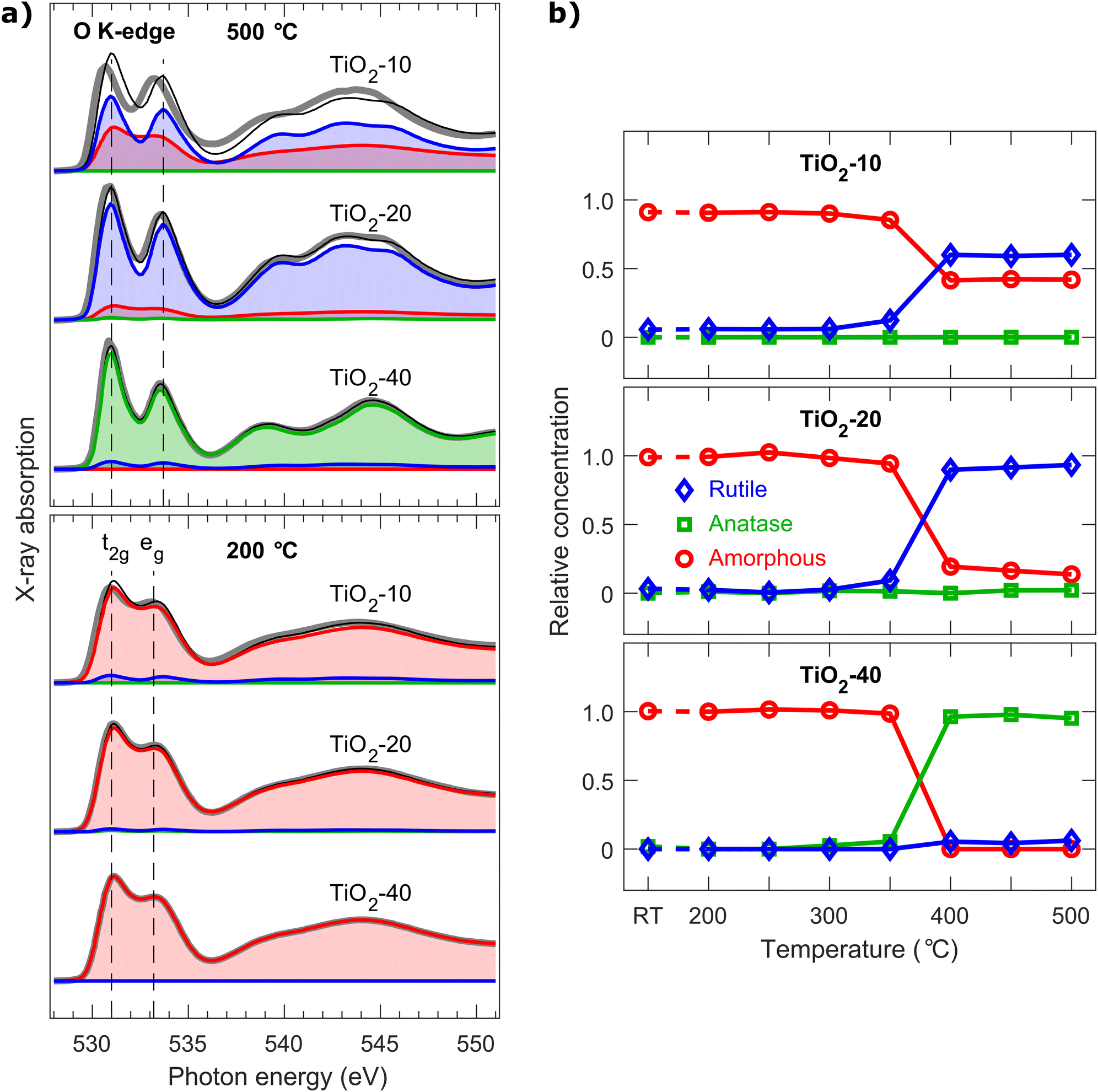 | ||
| Fig. 4 (a) NEXAFS total electron yield spectra of the O K-edge measured from the cumulative vacuum annealing series after 200 and 500 °C steps. The thick gray line represents the measured data. The spectra were fitted with amorphous (red), anatase (green) and rutile (blue) reference spectra and the thin black line is the sum of the fitted components. The reference spectra of anatase and rutile were recorded from samples with known crystallinity,5,41 whereas the spectra of the TiO2-10 sample after 200 °C annealing were used as a reference for the amorphous phase as it has the lowest density of defects. (b) The concentrations of amorphous, anatase, and rutile phases during the annealing series were calculated from the total yield data. All spectra and fittings are presented in Fig. S5 and S6† and the relative concentrations of the phases in Fig. S7.† | ||
NEXAFS spectroscopy results showed no significant difference between total electron yield and Auger electron yield spectra and thus we conclude that the phase of TiO2 is more or less the same in the bulk and at the surface. The results show that all the samples have similar NEXAFS spectra at the beginning of the annealing series. Based on the GIXRD and SEM measurements, this phase was identified to be amorphous. All samples remained amorphous until the 400 °C annealing temperature. This is contrary to our earlier research where Ti3+ defects have been caused by N doping,4 but is in line with the research where the crystallization was controlled by the O content of the initial amorphous TiO2 thin film.16 NEXAFS spectroscopy shows that at 400 °C the TiO2-40 sample crystallized into anatase and the TiO2-20 sample into rutile. This interpretation is also supported by the GIXRD and SEM results. According to NEXAFS fittings, the TiO2-10 sample had a mixed amorphous and rutile phase after vacuum annealing at 400 °C. The increase of the separation of the t2g and eg peaks is a clear sign of crystallization and thus supports the hypothesis that the TiO2-10 sample is at least partially crystallized.4,43
The peak ratio of t2g and eg peaks of defect free TiO2 should be 1.5 as both the orbitals should be unoccupied.43 However, a large number density of Ti3+ defects causes the t2g orbital to be partially occupied,4 which decreases the intensity of the t2g absorption peak. This is clearly visible in the TiO2-10 sample, especially after annealing at 500 °C, as the intensity of the t2g peak falls short compared to the fitted reference spectra. As the intensity of the t2g peak is similar in both total electron yield and Auger electron yield spectra, it can be concluded that there is no vast difference in the Ti3+ concentrations between the bulk and surface phases. The crystallite size of the sample remained below the detection limit of conventional GIXRD but partial crystallization was observed by NEXAFS spectroscopy as it is sensitive to the structure of the nearest neighbors.
By combining NEXAFS and XPS results, it can be shown that the crystallization of amorphous TiO2 during vacuum annealing depends on the number density of Ov and Ti3+ defects but the crystallization temperature was the same regardless of the defect concentration. TiO2 with no defects crystallizes into microcrystalline anatase, whereas TiO2 with a moderate number density of defects crystallizes into nanocrystalline rutile. Interestingly, TiO2 with a large number density of defects crystallizes into a mixed amorphous/nanocrystalline rutile phase. A similar result has been published for pulse laser deposited TiO2 films by Yajima et al.2 They demonstrated that the amorphous TiO2 deposited in low O2 pressure (0.1 Pa) results in the rutile phase and TiO2 deposited in moderate O2 pressure (1 Pa) results in the anatase phase after crystallization during annealing at 600 °C in N2. Also, the existence of amorphous domains in defect-rich black TiO2 has been realized by Kang et al.1
3.4 Chemical stability
The protective properties of the TiO2 thin films were tested by conducting electrochemical impedance spectroscopy (EIS) in 1.0 M NaOH (Fig. S8†). Fig. 5 shows the magnitude of the change of the complex impedance at 316 Hz during the test compared to the value at 0.5 h. The impedance at this frequency reflects the interfacial charge transfer processes within the TiO2/Si systems44 and the impedance at 316 Hz was found to be a suitable parameter for monitoring the degradation of the TiO2/Si electrodes. The results show that the amorphous as deposited TiO2 thin films are chemically unstable in 1.0 M NaOH as the impedance response changes rapidly already within the first few hours. After the stability tests, a complete dissolution of the amorphous TiO2 films was confirmed visually. The vacuum annealed samples were stable for up to 80 h. Interestingly, the annealed TiO2-10 sample that had the mixed amorphous/noncrystalline rutile structure was chemically stable. Annealing has also been shown to enhance the chemical stability of ALD TiO2 thin films as well.26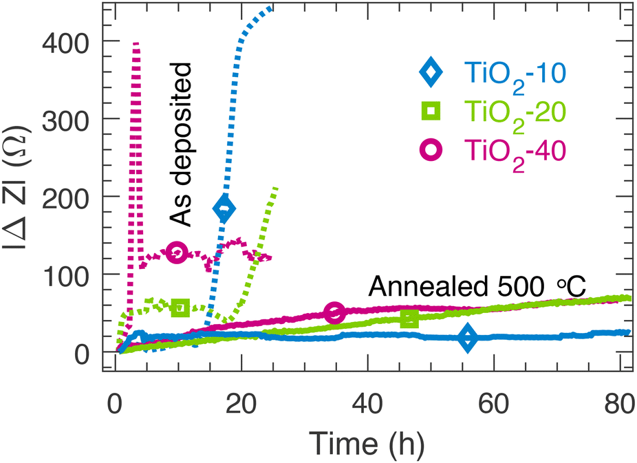 | ||
| Fig. 5 The change in impedance at 316 Hz during the stability tests in 1.0 M NaOH for the as deposited samples and the samples vacuum annealed at 500 °C. | ||
4 Conclusions
In this research, the effect of Ov and Ti3+ defects on vacuum annealing induced crystallization of TiO2 was studied. Amorphous TiO2 thin films were deposited using IBS and the Ov and Ti3+ defect concentrations were controlled by the O2 deficiency during the deposition. Interestingly, the O/Ti ratio was found to be close to the stoichiometric value of 2 and was not affected by the O2 deficiency and the formation of Ti3+ defects. The Ov and Ti3+ defects induced the formation of in-gap trap states that enhance the charge transfer properties of TiO2. After annealing in a vacuum, the sample with only a few defects crystallized into microcrystalline anatase with elongated grains, whereas the sample with a moderate number density of defects crystallized into nanocrystalline rutile. More importantly, the sample with an excessive number density of defects partially crystallized into rutile, thus featuring a mixed amorphous/rutile phase. The effect of the number density of defects on crystallization is summarized in Fig. 6. The defect concentration did not affect the crystallization temperature and all the samples crystallized at 400 °C. No decrease in the O/Ti ratio was observed after vacuum annealing even though the number density of Ti3+ and Ov defects increased, indicating the existence of under- and over-coordinated Ti atoms. Samples with a larger initial number density of Ti3+ defects also featured a larger increase in the number density during the vacuum annealing. The vacuum annealing increased the chemical stability of TiO2 in 1.0 M NaOH drastically. Most importantly, the mixed amorphous/nanocrystalline rutile phase was chemically stable, despite the amorphous phase that is typically considered unstable. This demonstrates that the crystallization and chemical stability of TiO2 can be controlled and engineered using Ov and Ti3+ defects. The high number of in-gap states after annealing due to the Ov and Ti3+ defects makes the charge transfer properties of TiO2 thin films suitable for photoelectrode coatings where both high chemical stability and good charge transfer properties are required. | ||
| Fig. 6 Schematic summary of the effect of Ov and Ti3+ defects on the crystallization of amorphous TiO2 during vacuum annealing. Unlike amorphous TiO2, the crystalline samples, including mixed phase Ti3+-rich amorphous/nanocrystalline rutile, were chemically stable in 1.0 M NaOH. | ||
Author contributions
J. R. fabricated the samples. L. P., M. H., and T. T. performed XAS and A. T. performed GIXRD and XRR. M. H. performed XPS and K. L. performed the stability tests. L. P. performed SEM and UV-vis, wrote the original draft of the manuscript, drew the figures, and analyzed the data. H. A.-L. analyzed the XRR data. H. A.-L., M. H., K. L., and M. V. participated in editing of the manuscript and M. V. and H. A.-L. supervised the work.Data availability
The data supporting this article have been included as part of the ESI.†Conflicts of interest
There are no conflicts of interest to declare.Acknowledgements
The authors thank Marika Janka for part of the IBS depositions. This work was supported by the Academy of Finland (decision no. 326461), Jane & Aatos Erkko Foundation (project “SOFUS”), and Business Finland (decision no. 1464/31/2019). L. P. was supported by the KAUTE Foundation, Finnish Cultural Foundation, Vilho, Yrjö and Kalle Väisälä Foundation of the Finnish Academy of Science and Letters, and Emil Aaltonen Foundation. H. A.-L. was supported by the Jenny and Antti Wihuri Foundation. T. T. was supported by the Academy of Finland (decision no. 339545, nSTAR consortium). This work is part of the Academy of Finland Flagship Programme, Photonics Research and Innovation (PREIN) (decision no. 320165). We acknowledge MAX IV Laboratory for time on the beamline FinEstBeAMS under proposals 20220486 and 20221303. Research conducted at MAX IV, a Swedish national user facility, was supported by the Swedish Research Council under contract 2018-07152, the Swedish Governmental Agency for Innovation Systems under contract 2018-04969, and Formas under contract 2019-02496.References
- J. Kang, Y. Zhang, Z. Chai, X. Qiu, X. Cao, P. Zhang, G. Teobaldi, L.-M. Liu and L. Guo, Adv. Mater., 2021, 33, 2100407 CrossRef CAS PubMed.
- T. Yajima, G. Oike, T. Nishimura and A. Toriumi, Phys. Status Solidi A, 2016, 213, 2196–2202 CrossRef CAS.
- C. Ros, T. Andreu, M. D. Hernández-Alonso, G. Penelas-Perez, J. Arbiol and J. R. Morante, ACS Appl. Mater. Interfaces, 2017, 9, 17932–17941 CrossRef CAS PubMed.
- L. Palmolahti, H. Ali-Löytty, M. Hannula, J. Saari, W. Wang, A. Tukiainen, K. Lahtonen and M. Valden, Acta Mater., 2022, 239, 118257 CrossRef CAS.
- H. Ali-Löytty, M. Hannula, J. Saari, L. Palmolahti, B. D. Bhuskute, R. Ulkuniemi, T. Nyyssönen, K. Lahtonen and M. Valden, ACS Appl. Mater. Interfaces, 2019, 11, 2758–2762 CrossRef PubMed.
- D. A. Hanaor and C. C. Sorrell, J. Mater. Sci., 2011, 46, 855–874 CrossRef CAS.
- D. O. Scanlon, C. W. Dunnill, J. Buckeridge, S. A. Shevlin, A. J. Logsdail, S. M. Woodley, C. R. A. Catlow, M. J. Powell, R. G. Palgrave and I. P. Parkin, et al. , Nat. Mater., 2013, 12, 798–801 CrossRef CAS PubMed.
- J. Saari, H. Ali-Löytty, M. M. Kauppinen, M. Hannula, R. Khan, K. Lahtonen, L. Palmolahti, A. Tukiainen, H. Gronbeck and N. V. Tkachenko, et al. , J. Phys. Chem. C, 2022, 126, 4542–4554 CrossRef CAS.
- F. G. Santomauro, A. Lübcke, J. Rittmann, E. Baldini, A. Ferrer, M. Silatani, P. Zimmermann, S. Grübel, J. A. Johnson and S. O. Mariager, et al. , Sci. Rep., 2015, 5, 14834 CrossRef CAS PubMed.
- B. J. Morgan and G. W. Watson, J. Phys. Chem. C, 2009, 113, 7322–7328 CrossRef CAS.
- B. Choudhury and A. Choudhury, Int. Nano Lett., 2013, 3, 1–9 CrossRef CAS.
- R. D. Shannon and J. A. Pask, J. Am. Ceram. Soc., 1965, 48, 391–398 CrossRef CAS.
- C. Rath, P. Mohanty, A. Pandey and N. Mishra, J. Phys. D: Appl. Phys., 2009, 42, 205101 CrossRef.
- K. Onda, B. Li and H. Petek, Phys. Rev. B: Condens. Matter Mater. Phys., 2004, 70, 045415 CrossRef.
- O. Agirseven, D. Rivella, J. Haggerty, P. Berry, K. Diffendaffer, A. Patterson, J. Kreb, J. Mangum, B. Gorman and J. Perkins, et al. , AIP Adv., 2020, 10, 025109 CrossRef CAS.
- O. Ağırseven, P. Biswas and J. Tate, J. Mater. Res., 2022, 37, 1135–1143 CrossRef.
- J. S. Mangum, O. Agirseven, J. E. Haggerty, J. D. Perkins, L. T. Schelhas, D. A. Kitchaev, L. M. Garten, D. S. Ginley, M. F. Toney and J. Tate, et al. , J. Non-Cryst. Solids, 2019, 505, 109–114 CrossRef CAS.
- T. Moehl, J. Suh, L. Severy, R. Wick-Joliat and S. D. Tilley, ACS Appl. Mater. Interfaces, 2017, 9, 43614–43622 CrossRef CAS PubMed.
- H. Li, T. Wang, S. Liu, Z. Luo, L. Li, H. Wang, Z.-J. Zhao and J. Gong, Angew. Chem., Int. Ed., 2021, 60, 4034–4037 CrossRef CAS PubMed.
- M. Björck and G. Andersson, J. Appl. Crystallogr., 2007, 40, 1174–1178 CrossRef.
- R. Pärna, R. Sankari, E. Kukk, E. Nõmmiste, M. Valden, M. Lastusaari, K. Kooser, K. Kokko, M. Hirsimäki and S. Urpelainen, et al. , Nucl. Instrum. Methods Phys. Res., Sect. A, 2017, 859, 83–89 CrossRef.
- B. Lafuente, R. T. Downs, H. Yang and N. Stone, in 1. The power of databases: The RRUFF project, ed. T. Armbruster and R. M. Danisi, De Gruyter (O), Berlin, München, Boston, 2016, pp. 1–30 Search PubMed.
- S. Sankar and K. Gopchandran, Cryst. Res. Technol., 2009, 44, 989–994 CrossRef CAS.
- XRD Crystallite (grain) Size Calculator (Scherrer Equation) – InstaNANO, https://instanano.com/all/characterization/xrd/crystallite-size, accessed 26.7.2023.
- S.-G. Wang, X.-D. Wen, D.-B. Cao, Y.-W. Li, J. Wang and H. Jiao, Surf. Sci., 2005, 577, 69–76 CrossRef CAS.
- M. Hannula, H. Ali-Löytty, K. Lahtonen, E. Sarlin, J. Saari and M. Valden, Chem. Mater., 2018, 30, 1199–1208 CrossRef CAS PubMed.
- S. Abdullah, M. Sahdan, N. Nafarizal, H. Saim, Z. Embong, C. C. Rohaida and F. Adriyanto, Appl. Surf. Sci., 2018, 462, 575–582 CrossRef CAS.
- G. Lu, A. Linsebigler and J. T. Yates Jr, J. Phys. Chem., 1994, 98, 11733–11738 CrossRef CAS.
- Z. Wang, B. Wen, Q. Hao, L.-M. Liu, C. Zhou, X. Mao, X. Lang, W.-J. Yin, D. Dai and A. Selloni, et al. , J. Am. Chem. Soc., 2015, 137, 9146–9152 CrossRef CAS PubMed.
- B. Bharti, S. Kumar, H.-N. Lee and R. Kumar, Sci. Rep., 2016, 6, 32355 CrossRef CAS PubMed.
- P. Makuła, M. Pacia and W. Macyk, J. Phys. Chem. Lett., 2018, 9, 6814–6817 CrossRef PubMed.
- J. Tauc, R. Grigorovici and A. Vancu, Phys. Status Solidi B, 1966, 15, 627–637 CrossRef CAS.
- C. E. Ekuma and D. Bagayoko, Jpn. J. Appl. Phys., 2011, 50, 101103 CrossRef.
- P. Chrysicopoulou, D. Davazoglou, C. Trapalis and G. Kordas, Thin Solid Films, 1998, 323, 188–193 CrossRef CAS.
- M. Landmann, E. Rauls and W. Schmidt, J. Phys.: Condens. Matter, 2012, 24, 195503 CrossRef CAS PubMed.
- E. Burstein, Phys. Rev., 1954, 93, 632 CrossRef CAS.
- Y. Nosaka and A. Y. Nosaka, J. Phys. Chem. Lett., 2016, 7, 431–434 CrossRef CAS PubMed.
- B. Avinash, V. Chaturmukha, H. Jayanna, C. Naveen, M. Rajeeva, B. Harish, S. Suresh and A. R. Lamani, AIP conference proceedings, 2016.
- V. Luca, J. Phys. Chem. C, 2009, 113, 6367–6380 CrossRef CAS.
- M. Sreemany and S. Sen, Mater. Chem. Phys., 2004, 83, 169–177 CrossRef CAS.
- R. Khan, H. Ali-Löytty, J. Saari, M. Valden, A. Tukiainen, K. Lahtonen and N. V. Tkachenko, Nanomaterials, 2020, 10, 1567 CrossRef CAS PubMed.
- M. Newville, Rev. Mineral. Geochem., 2014, 78, 33–74 CrossRef CAS.
- J. Chen, Surf. Sci. Rep., 1997, 30, 1–152 CrossRef CAS.
- M. Hannula, H. Ali-Löytty, K. Lahtonen, J. Saari, A. Tukiainen and M. Valden, Acta Mater., 2019, 174, 237–245 CrossRef CAS.
Footnote |
| † Electronic supplementary information (ESI) available: Additional materials characterization data. See DOI: https://doi.org/10.1039/d4nr03545c |
| This journal is © The Royal Society of Chemistry 2024 |