
 Open Access Article
 This Open Access Article is licensed under a
 Creative Commons Attribution 3.0 Unported Licence
A combined transient photovoltage and impedance spectroscopy approach for a comprehensive study of interlayer degradation in non-fullerene acceptor organic solar cells†
Adam
Pockett
 *,
Harrison Ka Hin
Lee
,
Brendan L.
Coles
,
Wing C.
Tsoi
and
Matthew J.
Carnie
*
*,
Harrison Ka Hin
Lee
,
Brendan L.
Coles
,
Wing C.
Tsoi
and
Matthew J.
Carnie
*
SPECIFIC – Swansea University, Materials Research Centre, College of Engineering, Bay Campus, Swansea, SA1 8EN, UK. E-mail: adam.pockett@swansea.ac.uk; m.j.carnie@swansea.ac.uk
First published on 28th May 2019
Abstract
Organic solar cells utilise thin interlayer materials between the active layer and metal electrodes to improve stability and performance. In this work, we combine transient photovoltage (TPV) and impedance spectroscopy (EIS) measurements to study how degradation affects both the active layer and the interlayer. We show that neither technique alone can provide a complete insight into both of these regions: TPV is more suited to studying degradation of the active layer; EIS clearly identifies the properties of the interlayer. By analysing both of these approaches we are able to assess how different interlayers impact the stability of the active layer, as well as how the interlayers themselves degrade and severely limit device performance. EIS measurements are also able to resolve the impact of the interlayer on series resistance even when it is not apparent from standard current–voltage (JV) measurements. The technique could therefore be valuable for the optimisation of all devices.
Introduction
Photovoltaic power production is dominated by silicon, a mature technology that has achieved many of the required milestones for successful commercialisation, namely high efficiency, low cost and excellent stability. In recent years, the research community has largely focused on perovskite solar cells. Perovskites are an exciting prospect, demonstrating high efficiencies and potential for low cost manufacture via solution processing. However, relatively poor stability is a major obstacle to widescale deployment. Both of these technologies also present concerns over the environmental impact of their manufacture. This pertains primarily to the energy intensive nature of high-quality silicon wafer production,1,2 and toxicity issues related to the presence of lead in perovskites.3,4Organic solar cells (OPV) have the potential to avoid many of these issues with the prospect of low embodies energy and low toxicity. The improvement of device efficiencies reached a plateau during the early part of this decade, but the development of non-fullerene acceptor (NFA) based devices has seen rapid progress on this front.5 As with many emergent PV technologies OPVs had long been seen as suitable for niche applications such as indoor energy harvesting and wearable technology,6,7 due to their low cost, light-weight, flexibility and solution processability. Efficiencies for fullerene-based bulk heterojunction (BHJ) devices were typically below 10%. NFA-based devices have now reached single junction efficiencies of around 15%,8 with tandem devices achieving 17%.9 If efficiencies continue to advance at this same rate, along with improved scaling of devices, then large scale energy production using OPV technology may become more feasible.
Another factor traditionally restricting OPV deployment has been their limited device stability, particularly with regards to photo-oxidation of the active layer due to ingress of oxygen and/or water.10–12 Other prominent degradation mechanisms exist including: reactions with the metal electrode,13,14 degradation at the ITO electrode,15 and thermal degradation due to low glass transition temperatures of the polymers.16,17 Many of these degradation processes can be mitigated with the use of effective barrier and encapsulation materials. However, this increases the cost and weight of devices thereby negating some of the potential benefits of OPVs. It is therefore desirable to maximize the intrinsic stability of the device so that minimal or no encapsulation is required.
With regards to the active layer, PCBM and other fullerene derivatives have been shown to readily photo-oxidize resulting in decreased performance due to the formation of trap states.18 Initial studies of NFA device stability suggest improved photo and thermal stability.19,20 The stability of contacts and interlayers within the device are also critical for long term operation. For example, it has been shown that replacement of the acidic and hygroscopic PEDOT:PSS hole-transport layer with nickel oxide can lead to improved stability.21,22
Interlayers between the active layers and metal electrodes play a multi-purpose role. Primarily, they are used to improve device performance by altering the electronic structure at the interface.23 Interlayers are added to improve the ohmic contact with the electrode by lowering the work function of the metal.24–26 Common interlayer materials include: low work function metals such as Ca, Ba, Mg; metal oxides such as MoO3 and TiOx; metal salts such as LiF; and organic polymers such as PFN and PEIE.23,27,28 As a secondary role, many of these interlayers also aid device stability by acting as a barrier to metal ion diffusion,29,30 as well as protecting the active layer from oxygen and moisture.31
It is clear that optimization of the interlayer is critical for good device performance, and also to understand how it impacts device stability. Optoelectronic characterisation techniques are often used to gain an understanding of device operation and assess new developments in device architecture. These techniques can be divided into two categories – time domain, and frequency domain measurements. Time resolved measurements include transient photovoltage/photocurrent (TPV/TPC) spectroscopy, charge extraction and space-charge limited current. Frequency domain techniques include electrochemical impedance spectroscopy (EIS) and associated techniques such as capacitance–voltage spectroscopy and Mott–Schottky analysis. Impedance spectroscopy has been widely used in the study of dye-sensitized solar cells (DSSC),32–34 but appears to be less common within the OPV community.35–37 Time domain techniques, predominantly TPV/TPC, seem to be favoured.38–42 In many scenarios the same information can be derived from either time or frequency domain measurements. However, the two are rarely performed in conjunction on the same devices to assess which processes either one may be best suited to studying, or what additional insight can be gained by using both.43
In this work, we perform both TPV/TPC and EIS measurements on regular architecture NFA based devices with different cathode interlayer (CIL) materials to study the impact this layer has on device stability. We show that TPV measurements are extremely useful in assessing the degradation of the active layer as a result of trap formation, while EIS measurements reveal more detail about the charge transport across the interlayer itself. By comparing the EIS response of devices with and without an interlayer present we are able to clearly identify the feature related to this layer, and are therefore able to assess its degradation. We find that inorganic interlayers are more susceptible to degradation, whether due to oxidation in the case of Ca or possibly reactions with the active layer for LiF. The degraded interlayers contribute a resistive barrier to charge extraction resulting in extremely high series resistance and a consequent s-shaped kink in the J–V curve. The organic interlayers studied show much greater resilience to direct degradation, and likewise seem to protect the active layer better. We also show that this technique could be useful in optimizing interlayer thicknesses.
Experimental
Materials
PEDOT:PSS (CLEVIOS P VP AI 4083) was purchased from Heraeus. PTB7-Th (poly[4,8-bis(5-(2-ethylhexyl)thiophen-2-yl)benzo[1,2-b;4,5-b′]dithiophene-2,6-diyl-alt-(4-(2-ethylhexyl)-3-fluorothieno[3,4-b]thiophene-)-2-carboxylate-2-6-diyl]) and ITIC (3,9-bis(2-methylene-(3-(1,1-dicyanomethylene)-indanone)-5,5,11,11-tetrakis(4-hexylphenyl)-dithieno[2,3-d:2′,3′-d′]-s-indaceno[1,2-b:5,6-b′]-dithiophene) were purchased from 1-Material. PFN-Br (poly[(9,9-bis(30-((N,N-dimethyl)-N-ethylammonium)-propyl)-2,7-fluorene)-alt-2,7-(9,9-dioctylfluorene)]dibromide) was purchased from Solarmer. PEIE (polyethylenimine, 80% ethoxylated solution) and all solvents were purchased from Sigma-Aldrich. All materials and solvents were used as received.Device fabrication
PEDOT:PSS was spin coated onto patterned ITO glass substrates and then followed by annealing on a 150 °C hotplate for 10 min. PTB7-Th and ITIC (1![[thin space (1/6-em)]](https://www.rsc.org/images/entities/char_2009.gif) :1.3 by weight) were dissolved in chlorobenzene with a total concentration of 17.5 mg ml−1 in a N2 filled glovebox at least 12 hours before spin coating. The PTB7-Th:ITIC solution was spin coated onto the PEDOT:PSS layers in the glovebox. Then, PEIE (0.3 wt% diluted in ethanol) or PFN-Br solution (0.5 mg ml−1 in methanol) were spin coated onto the active layers as the CIL. Finally, Al (100 nm) was thermally evaporated onto the samples in an evaporator with a base pressure of 10−5 mbar. CILs of Ca (30 nm) and LiF (1 nm) were evaporated in the same vacuum prior to the Al deposition. All devices were encapsulated before any measurement.
:1.3 by weight) were dissolved in chlorobenzene with a total concentration of 17.5 mg ml−1 in a N2 filled glovebox at least 12 hours before spin coating. The PTB7-Th:ITIC solution was spin coated onto the PEDOT:PSS layers in the glovebox. Then, PEIE (0.3 wt% diluted in ethanol) or PFN-Br solution (0.5 mg ml−1 in methanol) were spin coated onto the active layers as the CIL. Finally, Al (100 nm) was thermally evaporated onto the samples in an evaporator with a base pressure of 10−5 mbar. CILs of Ca (30 nm) and LiF (1 nm) were evaporated in the same vacuum prior to the Al deposition. All devices were encapsulated before any measurement.
Characterisation
The devices were characterised under an AM1.5G solar simulator for the standard one sun performance. The devices were put into an environmental chamber with a continuous flow of N2 under white LED arrays to achieve one sun equivalent performance (calibrated using the Jsc values obtained from the one sun measurements).TPV measurements were performed using a commercially available transient measurement system (Automatic Research GmbH). This system uses a 520 nm green laser diode driven by a waveform generator (Keysight 33500B) to give a 300 ns pulse length. Background illumination was provided by a white LED with its intensity calibrated to generate the same device photocurrent as measured using the solar simulator – this intensity is referred to as ‘1 Sun equivalent’. An intensity range was then calibrated using a silicon photodiode. Transient responses were captured by a digital storage oscilloscope (Keysight DSOX2024A), the number of sample averages being adjusted to optimise signal noise and measurement time. The device under test was held at open-circuit by a custom-built voltage follower (1.5 TΩ input impedance). TPC measurements were performed by measuring the voltage drop across a 50 Ω resistor.
EIS measurements were carried out using a Gamry Reference 600 instrument. Measurements were performed at the open-circuit potential over the same intensity range as used in the TPV measurements. A 10 mV ac amplitude was used over a frequency range from 1 MHz to 1 Hz. Fitting to the experimental data was performed using ZView software (Scribner Associates).
Results and discussion
Device performance and degradation
We built a series of regular architecture BHJ devices based on the NFA small molecule ITIC and polymer donor PTB7-Th, with a range of different CIL materials. The interlayers chosen represented a selection of some of the most common organic and inorganic materials used in OPV devices, which included: Ca, LiF, PEIE, PFN-Br and control devices without an interlayer between the active layer and the Al cathode. Fig. 1 shows the JV curves obtained from these cells when measured under illumination from a white LED providing 1 Sun equivalent intensity (see Experimental section for definition. JV curves and extracted parameters measured under 1 Sun AM1.5 conditions can be found in the ESI†). From these measurements it is clear that the different interlayers, in otherwise identical cells, alter the electrical performance of the device. The presence of each of the interlayers creates a clear increase in Voc of around 150 mV relative to the control device, consistent with the understanding that the interlayers are used to modify the work function of the cathode, thus improving the ohmic nature of the contact resulting in an increase in Voc.44 Other effects of the interlayers on device performance are less clear, with relatively consistent Jsc and FF for all devices. One exception is for the FF of the LiF device – the presence of an s-shaped kink in the JV curve near Voc can be seen, which reduces the FF considerably. This is likely due to the LiF layer being too thick as seen in other reports.45,46 | ||
| Fig. 1 Current–voltage curves of fresh (solid lines) and degraded cells (dashed lines) with different interlayers, measured under illumination from a white LED of 1 Sun equivalent intensity. Note: See ESI† for JV curves and extracted parameters of fresh devices measured under 1 Sun AM1.5 illumination. | ||
Encapsulated devices were degraded for 65 hours under white LED illumination of 1 Sun equivalent intensity. Encapsulation ensured that the rate of degradation was slow enough so as to ensure a range of optoelectronic characterisation techniques could be performed without degradation occurring between the different measurements. The degraded device JV curves are also shown in Fig. 1. Each of the different interlayer devices show s-shaped kinks once degraded, whilst it is not present for the device without an interlayer. This is an initial indication that the s-shape is related to the interlayer as there is a clear distinction in the shape of the JV curve for cells with and without a CIL. The extracted JV parameters for both fresh and degraded devices are compared in Fig. 2 (plots tracking the degradation over time can be found in the ESI†). Although the devices were encapsulated, the significant degradation observed suggests that it was not fully successful in protecting the device from oxygen and moisture ingress. It is clear that the degradation has the most significant effect on FF and Jsc, which combined give a substantial reduction in efficiency. As expected, devices which show the s-shaped kink have a correspondingly low fill-factor – the reduction in fill factor is less significant for the interlayer free device upon degradation. The Voc appears to be least affected by the degradation, a possible indication that the performance loss is more related to charge extraction rather than an increase in recombination. Indeed, even for the LiF device with a highly pronounced s-shape in the JV curve after degradation, the Voc has only dropped by around 50 mV despite FF and Jsc losses of more than 50%.
 | ||
| Fig. 2 Parameters extracted from the J–V curves shown in Fig. 1 for fresh (filled symbols) and degraded cells (open symbols). Note: Efficiencies are approximate values assuming 1 Sun equivalent light intensity. | ||
Transient photovoltage measurements
A deeper understanding of the device operation, and in particular the impact of degradation was gained by performing a range of optoelectronic characterisation measurements on the devices. The same devices were measured when fresh and once degraded to rule out changes caused by batch to batch variation. TPV and TPC measurements were performed over a range of light intensities from 1 Sun equivalent to 0.001 Sun equivalent. The charge carrier density was calculated by integrating the capacitance with respect to voltage, with the capacitance calculated using the differential charging method38where ΔQ is obtained from the integral of the TPC decay and ΔV is the amplitude of the TPV transient, for the same laser pulse intensity. The charge density, n, is plotted as a function of Voc in Fig. 3a for the fresh and degraded cells. For fresh cells, there is good agreement between the charge densities calculated for each of the devices with an interlayer, whilst the control device shows a lower Voc despite comparable charge density. This is consistent with the interlayers creating an energetic shift at the electrode by decreasing the work function of the metal. An increase in charge density for a given Voc can be observed for all devices upon degradation, indicative of an increase in trap density – potentially caused by photo-oxidation of the active layer materials or reactions caused near the interface as a result of the interlayer degradation. There is a spread in the magnitude of this increase dependent on the interlayer, which allows us to assess how an interlayer may act as a barrier to this particular degradation route. The most significant increase in trap density occurs for the interlayer-free device with over a 20-times increase in charge density at a Voc of 0.55 V. This suggests that the active layer is most severely affected when there is no interlayer to act as a buffer against either Al diffusion or oxygen/moisture ingress. Ca and LiF devices show similar high levels of increase in charge density which may be due to a number of factors: Ca has been shown to readily degrade in the presence of oxygen and moisture which can lead to the formation of voids near the electrode;47,48 thin LiF layers do not provide complete coverage and protection of the active layer;45,49 dissociation of LiF resulting in doping or chemical reactions.50,51 PFN-Br and PEIE appear to provide the most resilience against trap formation with increases in trap densities compared to fresh devices of 7 and 3-times respectively. The increases in charge density upon degradation for each of the devices are consistent with the observed changes in Voc. An increased trap density results in a lower quasi-Fermi level splitting for a given amount of charge in the device (i.e. for a given light intensity). PEIE and PFN-Br devices show the least significant increase in charge density, in agreement with those devices showing the smallest decrease in Voc (see Fig. 2). The interlayer free and inorganic interlayer devices show more substantial charge density increases and therefore have greater losses in Voc.

 | ||
| Fig. 3 Charge density, n, as a function of Voc for fresh and degraded cells (a), and recombination lifetimes, τ, extracted from TPV measurements as a function of charge density for fresh and degraded cells (b). | ||
All devices gave single exponential TPV decays in response to the small amplitude laser pulse perturbation. The time constants obtained from fitting single exponential functions to these decay curves are taken to be the carrier lifetimes, τ, and are plotted as a function of charge density in Fig. 3b. These results are consistent with the increase in trap formation with degradation as carrier lifetimes are shown to increase for given carrier densities. This is evidence that charges spend a certain amount of time in these traps, before being released and being able to recombine. These traps are therefore likely to be shallow traps that do not act as recombination centres. The increased carrier lifetime does not result in an increase in Voc for degraded devices as a much higher charge density would now be needed to reach the same Fermi-level splitting as in fresh devices. There is some dispersion in the trends of carrier lifetime versus Voc but in general lifetimes are similar for all devices, especially near to 1 Sun intensity, which indicates that the interlayer properties don't have a significant influence on recombination kinetics. It is possible that the increased trap density may have an impact on the FF of the devices, which is one of the main losses as a result of degradation, but as recombination is also slowed down by this process it may not lead to significant losses in charge collection efficiency.
As we have not observed significant changes in recombination behaviour, including in the devices ideality factor (see ESI†), the observed performance degradation is unlikely to be as a result of energy level changes. Energy level shifts at the cathode contact would alter the devices built-in field and likely limit the Voc. We have shown that the relatively modest change in Voc is consistent with the formation of trap states within the active layer. We also do not observe increases in recombination or specifically the presence of surface recombination which would be the result of changes in energy level profile near the contact.52
These time domain measurements can be seen as being very useful in analysing the properties of the device active layer. The presence or quality of the interlayer does not directly affect the clarity of this measurement as TPV measurements are carried out with the device held at open-circuit by a very large resistance – no charge is extracted through the electrode. In this case we can confirm that the degradation does not induce significant increases in trap-assisted recombination which may be one potential source of performance loss. The technique can be used to analyse the differences in degradation of the active layer due to the presence of interlayers, some of which may perform better than others as barriers to oxygen or moisture ingress.
Impedance spectroscopy measurements
Time and frequency domain measurements, such as TPV and EIS, are often employed to study recombination in devices, and in many cases would produce comparable results.53–55 These techniques have been widely employed in DSSC research,32–34,56 although not often in combination. Studies are predominately published where either the frequency or time domain characterisation techniques are favoured. In this work, we performed EIS measurements on the same devices studied by TPV in an attempt to get further insights into the role of the interlayer degradation on device performance. Whilst we also perform EIS measurements at open-circuit under illumination, this is not a galvanostatic measurement. The open-circuit potential is applied to the cell under illumination, with a small amplitude ac perturbation superimposed. Therefore current is extracted from the device as the potential oscillates either side of the open-circuit condition. This makes it more likely that contact effects will be observed in EIS measurements, rather than in TPV where all charges recombine within the device.The first assessment to be made from the EIS studies is associating a physical process to the measured response – essentially to determine if a process relating to the interlayer can be observed on the timescales probed by EIS. The impedance response of the control device without an interlayer and device with a Ca interlayer is shown in Fig. 4. Only one process is visible in the control cell response, represented by the single semi-circle in the Nyquist plot, and only one maximum in the phase angle of the Bode plot. However, for the Ca cell two processes can be observed; one at high frequency with a phase angle maximum at around 5 × 10⁵ Hz, and a lower frequency feature at 4 × 10⁴ Hz. The high frequency feature is consistent with the single processed observed in the control cell. All of the devices with an interlayer present display these two processes in the impedance response, whereas only a single high frequency feature is observed for the cell without an interlayer (only one process can be resolved in the fresh PFN-Br device, but the second feature becomes apparent upon degradation as discussed below). This is the first indication that the low frequency process is related to the interlayer.
 | ||
| Fig. 4 Nyquist and Bode plots for fresh interlayer-free and Ca cells measured under 1 Sun equivalent illumination. Peaks in the phase angle relating to the high frequency (HF) and lower frequency (LF) processes are labelled (impedance magnitude is plotted in grey). | ||
After degradation, a single process is still observed for the interlayer-free device as shown in Fig. 5a. For cells with an interlayer the low frequency feature becomes more pronounced, with large increases in its corresponding resistance. Fig. 5b shows the EIS response for the fresh and degraded PFN-Br device. For this device, only a single process is observed when fresh although the low frequency feature becomes visible in the degraded device. This likely indicates that this interlayer has a very low resistance when fresh, consistent with this device having the highest FF, so the second lower frequency process is obscured by the high frequency feature.
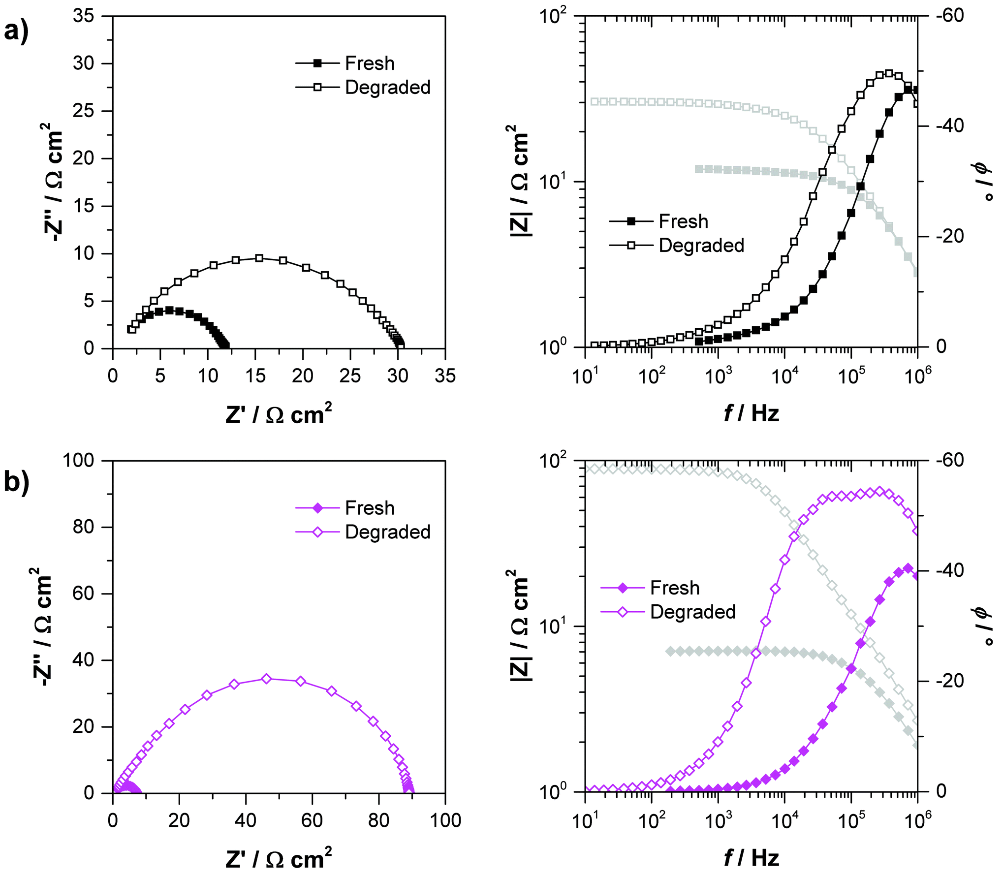 | ||
| Fig. 5 Nyquist and Bode plots for fresh and degraded cells without an interlayer (a), and for PFN-Br interlayer cells (b) measured under 1 Sun equivalent illumination. | ||
Taking the above observations of the EIS response into account we fitted the data to the equivalent circuit shown in Fig. 6. A series resistance element, Rs, is included which accounts for the sheet resistance of the ITO and connecting wires (N.B. this series resistance is not linked to the series resistance often discussed from JV analysis). The parallel combination of Rrec and Cμ represents the recombination resistance (inversely proportional to the recombination rate) and chemical capacitance (accumulation of charge within the device) respectively. For devices with an interlayer the additional lower frequency process is modelled by the parallel combination of Rint and Cint representing the interlayer resistance and capacitance respectively.
 | ||
| Fig. 6 Equivalent circuit used to model impedance data. ‘Interlayer’ components are including for devices with an interlayer present when the feature can be resolved. | ||
We performed a number of checks to validate this model. Firstly, the time constant obtained for the high frequency feature, τ = RrecCμ, should relate to the recombination lifetime obtained from the TPV measurements. The time constants found from both of these techniques for a fresh PFN-Br device are shown in Fig. 7. Good agreement can be seen between the two techniques for all but the highest light intensities – the lifetimes obtained by EIS begin to plateau. This could be related to EIS being unsuitable for measuring very short lifetimes as the stray capacitance from the cabling and connections (likely a few nanofarads) results in an RC limit, which will present as a phase shift that is not related to the actual recombination process.
 | ||
| Fig. 7 EIS high frequency time constant compared to carrier lifetimes extracted from TPV measurements. The good agreement confirms that the high frequency process observed in EIS is linked to recombination. | ||
We also carefully evaluated the fit results for a fresh LiF device over a range of light intensities to confirm that the fit parameters had the expected relationships with change in Voc. The fitting process is complicated by the need to replace the capacitors in Fig. 6 by constant phase elements (CPE) to model capacitive behaviour for non-ideal systems, which then requires the calculation of an equivalent capacitance from the CPE parameters. In order to show that the perceived trends are real, and not an artefact of the fitting process or calculation of the equivalent capacitance, we performed error analysis from the uncertainty values on the fit parameters obtained by least-squares regression – including propagation of the errors through the equivalent capacitance calculation. A more in-depth discussion on the fitting parameters, error calculations and the uncertainty in fitting the two processes is given in the ESI.† It can be seen that within error the high frequency capacitance increases exponentially with increasing Voc, consistent with the expected behaviour of a chemical capacitance. It should be noted that at high Voc the extraction of this capacitance is also hindered by the RC effects described for the time constant of the recombination process. We also confirmed that the low Voc plateau in capacitance is related to the geometric capacitance of the device. The low frequency capacitance remains roughly constant across the voltage range, consistent with an interlayer capacitance. The strong dependence of the high frequency resistance on light intensity is also in agreement with that element representing a recombination resistance. The much weaker dependence on the Voc for the low frequency resistance shows that this process is not related to a recombination mechanism and is linked to the resistance of the interlayer. The weak dependence on Voc may suggest that there is also a presence of traps at the interface, essentially resulting in a higher conductivity when they are filled. As shown from the TPV measurements, these trap states do not appear to contribute to increased recombination.
The above assessment of the physical relevance of the equivalent circuit employed therefore allows us to draw conclusions on the operation of these devices and the impact of degradation. We have shown that the two processes in the impedance response are related to recombination in the active layer at high frequency, and the interlayer resistance and capacitance at low frequency.
Analysis of the two resistance components provides useful insight into the relative performance of the devices when fresh. It can be seen from the JV results (Fig. 1 and 2) that the LiF device has a low FF, mainly due to an apparent high series resistance (being inversely proportional to the slope of the JV curve at Voc) resulting in the s-shaped kink. We can use EIS to analyse this particular feature of the JV curve by considering the total resistance of the device. The total resistance of the cell is taken to be the low-frequency (or ‘dc’) limit of the impedance response (Rdc = Rs + Rrec + Rint) which is equivalent to the inverse of the slope of the JV response at Voc

The resistance values obtained from the EIS fitting for the LiF device are shown in Fig. 8. For the fresh cell, the interlayer resistance is 57 Ω cm2 – an order of magnitude higher than the recombination resistance. This results in a high Rdc, as also observed in the JV response. Therefore, using the impedance analysis we are able to determine that the high series resistance is predominantly due to the resistance of the interlayer, highlighting an important area for optimisation. It is likely that the high resistance in this case is due to the interlayer being too thick (the effect of interlayer thickness on Rint is shown in the ESI†). The interlayer resistances determined for the Ca and PEIE devices were 23 and 10 Ω cm2 respectively. These values were not high enough to create the s-shaped JV response, but do contribute to slightly lower fill factors compared to the PFN-Br device from which we did not observe the interlayer resistance for fresh devices by EIS as it was too small compared to the recombination resistance to be resolved. The fact that the low frequency process can be observed even in cells not displaying the s-shaped behaviour highlights that this could be an extremely useful technique for device optimisation when the effects only result in very minor differences in JV performance.
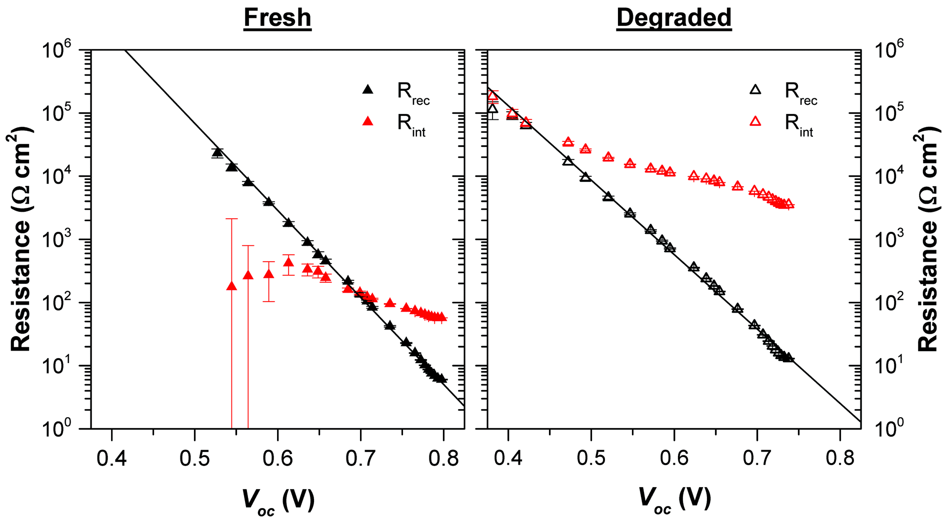 | ||
| Fig. 8 Values of the recombination and interlayer resistances for a fresh and degraded LiF device. See ESI† for discussion on uncertainties in fitting the two processes. | ||
The EIS measurements also show that degradation predominantly impacts the interlayer resistance (Fig. 8). As found from the TPV measurements, degradation has a relatively minor impact on the properties of the active layer as seen from the modest changes observed in the high frequency response. For a given Voc, the recombination resistance decreases upon degradation, for example at Voc = 0.65 V the recombination resistance decreases from 600 Ω cm2 to 150 Ω cm2. This suggests an increase in the recombination rate, but as we observed an increase in trap density using the TPV measurements, there will be a higher charge density in the degraded device at this Voc accounting for this increased recombination.
Compared to the recombination behaviour, the degradation results in significant increases in the interlayer resistance. At 1 Sun intensity the interlayer resistance increases to 3.5 kΩ cm2 in the degraded device. Such a large interlayer resistance results in the severe loss of FF and Jsc seen for the degraded LiF device.
The degradation of the LiF interlayer can be compared to the other materials tested. The Ca and PEIE interlayers both show significant increases in resistance to 250 and 127 Ω cm2 respectively, although this only equates to around a 10-fold increase upon degradation compared to 60-fold for the LiF device. As shown in Fig. 5b the contact effects are not observed for the PFN-Br cell when fresh, but the low frequency process is visible when the cell has been degraded. The interlayer resistance for the degraded PFN-Br cell is 82 Ω cm2, representing more than a 10-fold increase as the interlayer resistance for the fresh cell was less than 7 Ω cm2 (although it wasn't resolved in the fresh cell, Rint must have been less than Rdc). It is possible that low resistance contact processes could be observed in fresh cells if measured at intensities above 1 Sun, which will decrease the recombination resistance further, allowing the contact effects to be resolved.
These results are consistent with the finding that the s-shaped JV response is only observed in fresh devices with the LiF interlayer. All other devices have interlayer resistances of 23 Ω cm2 or less, which does not appear to be significant enough to cause the kink in the JV curve. The PFN-Br device has a very low interlayer resistance which is consistent with it having the highest fill factor. All of the interlayer devices show the s-shape JV characteristics upon degradation, due to them all having greater than 82 Ω cm2 interlayer resistance. The degraded LiF device has a very low FF due to its extremely high interlayer resistance of 3.5 kΩ cm2. The control device does not show the s-shape behaviour when fresh or degraded as it does not contain an interlayer to contribute the high resistances observed for the other devices.
Discussion
The results presented here show that extensive information can be gained by using the time and frequency domain techniques in conjunction, that otherwise might be overlooked if one technique was favoured over the other. Broadly, their suitability for studying particular processes within the device can be split into two areas: (i) TPV measurements are capable of resolving small changes in active layer properties, such as charge density and recombination lifetimes; (ii) EIS measurements show the effect of interlayer and contact properties on current extraction from the device. Neither technique can provide a complete insight into both active layer and interlayer/contact effects – even though EIS can resolve both processes, TPV is shown to be more suited to measuring fast recombination lifetimes.The TPV results show the effect of degradation on trap formation and recombination. It was shown that the level of degradation with regards to trap formation varied between the different interlayers, suggesting that the organic polymer layers provided more resilience against this particular degradation route. Thin interlayers such as LiF do not provide a suitable barrier to oxygen and moisture ingress.45,49 Ca readily reacts with oxygen and moisture, which has been shown to create voids at the interface with the active layer which may also contribute to trap states.47 However, this increase in trap density was not found to increase recombination in the device. Considering the extensive deterioration in device performance upon degradation, these findings do not account for the observed losses particularly with regards to FF.
EIS measurements reveal the presence of two processes for devices with an interlayer present. We have shown through careful assessment of the impedance response that these two processes relate to recombination in the active layer (corresponding well to the TPV measurements) and charge transport at the interlayer. A high interlayer resistance is shown to be linked to the appearance of the s-shape JV behaviour as seen in the fresh LiF device. The interlayer resistance is shown to increase substantially upon degradation resulting in the s-shape kink in the JV curves of all devices with an interlayer. Fig. 9 highlights the significance of the interlayer in contributing to the total device series resistance. A high series resistance leads to the s-shape JV behaviour and substantially decreased FF. For the fresh devices, the LiF interlayer is found to contribute almost 90% of the total cell resistance showing this device interlayer is clearly unoptimized. This suggests that the LiF interlayer is too thick considering it's insulating properties (we show in the ESI† the dependence of Rint on the interlayer thickness). Whilst not displaying the s-shape behaviour the Ca and PEIE interlayers still contribute significantly to the devices series resistance and could be further optimized. The PFN-Br interlayer does not appear to negatively affect the series resistance of the fresh cell.
 | ||
| Fig. 9 Percentage contribution of the interlayer resistance to the total series resistance of the devices for fresh and degraded cells at 1 Sun intensity. | ||
Degradation of all the interlayers is significant, which leads to the interlayer resistance dominating the response of the cells. The exact nature of the degradation of the inorganic layers is unclear, but clearly leads to a large reduction in their conductivity. The degradation of Ca may lead to the formation of CaO, or even Ca(OH)2, which have insulating characteristics. The formation of voids at the interface with the interlayer will also reduce the effective conductivity.47 The LiF interlayer undergoes the most significant degradation as shown by the 60-fold increase in Rint. This resistance accounts for practically 100% of the total cell series resistance and results in a JV curve with a severe s-shaped kink. LiF has been shown to dissociate in a reaction with aluminium, and even form the insulator AlF3 which may account for this increase in resistance.57,58 Interestingly, this cell maintains a reasonable Voc showing that the dominant degradation loss is not linked to recombination. The loss in Jsc relative to the other devices is also likely due to the series resistance being over an order of magnitude higher resulting in a significant voltage drop under short circuit conditions.59
In addition to the apparent improved stability of devices containing an organic interlayer, particularly in the case of PEIE, there are a number of additional benefits. Primarily, the solution processability of the organic layers favours large scale printing deposition rather than the need for high cost vacuum deposition of inorganic materials.60,61 Organic molecules also have a greater degree of tunability with regards to properties such as conductivity and energy level alignment.28 The techniques demonstrated in this work could be of considerable use in comparing new interlayer materials with regards to performance and stability, by examining the compromise between reduced series resistance and increased barrier performance to degradation processes such as photo-oxidation of the active layer and metal migration.
Conclusions
We have demonstrated the use of a combination of both time and frequency domain optoelectronic characterisation techniques to gain a deeper insight into the behaviour and degradation of OPV devices with respect to the cathode interlayer material used. The two techniques are capable of studying different regions of the device in detail. TPV measurements reveal information about recombination processes occurring primarily within the active layer of the device. EIS measurements were used to clearly identify the impact the interlayer has on device performance, and how different interlayers are affected by degradation.TPV measurements show that degradation causes an increase in trap density in the active layer. Organic interlayers appear to protect the active layer of the device better than inorganic materials, as the increase in trap density is lower.
Through careful assessment of the impedance response we showed that the effect of the interlayer on charge extraction from the device can be observed; interlayers that are too thick, as well as interlayer degradation, contribute significantly to the devices series resistance. The technique could therefore be extremely useful in the optimisation of many devices. The high resolution of the EIS technique means that improvements of less than 1 Ω cm2 can be analysed, which could be significant, especially for high performance devices. The technique could also be employed in large area module testing with similar hardware, whereas laser spectroscopies such as TPV are more difficult to scale and would require time consuming x–y mapping.
Notes
All data created during this research are openly available from the Swansea University data archive at 10.5281/zenodo.2591435.Conflicts of interest
There are no conflicts to declare.Acknowledgements
The authors would like to thank the EPSRC (EP/N020863/1, EP/R032750/1, EP/M025020/1), the Welsh European Funding Office (SPARC II) and the Welsh Government's Sêr Solar programme for funding.Notes and references
- M. J. de Wild-Scholten, Sol. Energy Mater. Sol. Cells, 2013, 119, 296–305 CrossRef CAS
.
- S. A. Mann, M. J. de Wild-Scholten, V. M. Fthenakis, W. G. J. H. M. van Sark and W. C. Sinke, Prog. Photovoltaics, 2014, 22, 1180–1194 Search PubMed
- A. Abate, Joule, 2017, 1, 659–664 CrossRef CAS
- B. Hailegnaw, S. Kirmayer, E. Edri, G. Hodes and D. Cahen, J. Phys. Chem. Lett., 2015, 6, 1543–1547 CrossRef CAS PubMed
- J. Hou, O. Inganäs, R. H. Friend and F. Gao, Nat. Mater., 2018, 17, 119 CrossRef CAS PubMed
- H. K. H. Lee, J. Wu, J. Barbé, S. M. Jain, S. Wood, E. M. Speller, Z. Li, F. A. Castro, J. R. Durrant and W. C. Tsoi, J. Mater. Chem. A, 2018, 6, 5618–5626 RSC
- H. K. H. Lee, Z. Li, J. R. Durrant and W. C. Tsoi, Appl. Phys. Lett., 2016, 108, 253301 CrossRef
- J. Yuan, Y. Zhang, L. Zhou, G. Zhang, H.-L. Yip, T.-K. Lau, X. Lu, C. Zhu, H. Peng, P. A. Johnson, M. Leclerc, Y. Cao, J. Ulanski, Y. Li and Y. Zou, Joule, 2019, 3, 1140–1151 CrossRef CAS
- L. Meng, Y. Zhang, X. Wan, C. Li, X. Zhang, Y. Wang, X. Ke, Z. Xiao, L. Ding, R. Xia, H.-L. Yip, Y. Cao and Y. Chen, Science, 2018, 361, 1094–1098 CrossRef CAS PubMed
- J. Schafferhans, A. Baumann, A. Wagenpfahl, C. Deibel and V. Dyakonov, Org. Electron., 2010, 11, 1693–1700 CrossRef CAS
- M. Manceau, E. Bundgaard, J. E. Carlé, O. Hagemann, M. Helgesen, R. Søndergaard, M. Jørgensen and F. C. Krebs, J. Mater. Chem., 2011, 21, 4132–4141 RSC
- A. Seemann, H. J. Egelhaaf, C. J. Brabec and J. A. Hauch, Org. Electron., 2009, 10, 1424–1428 CrossRef CAS
- M. Wang, F. Xie, J. Du, Q. Tang, S. Zheng, Q. Miao, J. Chen, N. Zhao and J. B. Xu, Sol. Energy Mater. Sol. Cells, 2011, 95, 3303–3310 CrossRef CAS
- M. T. Lloyd, D. C. Olson, P. Lu, E. Fang, D. L. Moore, M. S. White, M. O. Reese, D. S. Ginley and J. W. P. Hsu, J. Mater. Chem., 2009, 19, 7638–7642 RSC
- M. P. d. Jong, L. J. v. IJzendoorn and M. J. A. d. Voigt, Appl. Phys. Lett., 2000, 77, 2255–2257 CrossRef
- I. T. Sachs-Quintana, T. Heumüller, W. R. Mateker, D. E. Orozco, R. Cheacharoen, S. Sweetnam, C. J. Brabec and M. D. McGehee, Adv. Funct. Mater., 2014, 24, 3978–3985 CrossRef CAS
- B. Conings, S. Bertho, K. Vandewal, A. Senes, J. D'Haen, J. Manca and R. A. J. Janssen, Appl. Phys. Lett., 2010, 96, 163301 CrossRef
- H. K. H. Lee, A. M. Telford, J. A. Röhr, M. F. Wyatt, B. Rice, J. Wu, A. de Castro Maciel, S. M. Tuladhar, E. Speller, J. McGettrick, J. R. Searle, S. Pont, T. Watson, T. Kirchartz, J. R. Durrant, W. C. Tsoi, J. Nelson and Z. Li, Energy Environ. Sci., 2018, 11, 417–428 RSC
- W. Zhao, D. Qian, S. Zhang, S. Li, O. Inganäs, F. Gao and J. Hou, Adv. Mater., 2016, 28, 4734–4739 CrossRef CAS PubMed
- D. Baran, R. S. Ashraf, D. A. Hanifi, M. Abdelsamie, N. Gasparini, J. A. Röhr, S. Holliday, A. Wadsworth, S. Lockett, M. Neophytou, C. J. M. Emmott, J. Nelson, C. J. Brabec, A. Amassian, A. Salleo, T. Kirchartz, J. R. Durrant and I. McCulloch, Nat. Mater., 2016, 16, 363 CrossRef PubMed
- M. D. Irwin, D. B. Buchholz, A. W. Hains, R. P. H. Chang and T. J. Marks, Proc. Natl. Acad. Sci. U. S. A., 2008, 105, 2783–2787 CrossRef CAS
- J. R. Manders, S.-W. Tsang, M. J. Hartel, T.-H. Lai, S. Chen, C. M. Amb, J. R. Reynolds and F. So, Adv. Funct. Mater., 2013, 23, 2993–3001 CrossRef CAS
- T.-H. Lai, S.-W. Tsang, J. R. Manders, S. Chen and F. So, Mater. Today, 2013, 16, 424–432 CrossRef CAS
- M. O. Reese, M. S. White, G. Rumbles, D. S. Ginley and S. E. Shaheen, Appl. Phys. Lett., 2008, 92, 053307 CrossRef
- Z. He, C. Zhong, S. Su, M. Xu, H. Wu and Y. Cao, Nat. Photonics, 2012, 6, 591 CrossRef
- C. J. Brabec, S. E. Shaheen, C. Winder, N. S. Sariciftci and P. Denk, Appl. Phys. Lett., 2002, 80, 1288–1290 CrossRef CAS
- R. Steim, F. R. Kogler and C. J. Brabec, J. Mater. Chem., 2010, 20, 2499–2512 RSC
- Z. Yin, J. Wei and Q. Zheng, Adv. Sci., 2016, 3, 1500362 CrossRef PubMed
- K. Suemori, M. Yokoyama and M. Hiramoto, J. Appl. Phys., 2006, 99, 036109 CrossRef
- M. O. Reese, A. J. Morfa, M. S. White, N. Kopidakis, S. E. Shaheen, G. Rumbles and D. S. Ginley, Sol. Energy Mater. Sol. Cells, 2008, 92, 746–752 CrossRef CAS
- K. Lee, J. Y. Kim, S. H. Park, S. H. Kim, S. Cho and A. J. Heeger, Adv. Mater., 2007, 19, 2445–2449 CrossRef CAS
- Q. Wang, J.-E. Moser and M. Grätzel, J. Phys. Chem. B, 2005, 109, 14945–14953 CrossRef CAS PubMed
- F. Fabregat-Santiago, J. Bisquert, G. Garcia-Belmonte, G. Boschloo and A. Hagfeldt, Sol. Energy Mater. Sol. Cells, 2005, 87, 117–131 CrossRef CAS
- F. Fabregat-Santiago, J. Bisquert, E. Palomares, L. Otero, D. Kuang, S. M. Zakeeruddin and M. Grätzel, J. Phys. Chem. C, 2007, 111, 6550–6560 CrossRef CAS
- G. Garcia-Belmonte, P. P. Boix, J. Bisquert, M. Sessolo and H. J. Bolink, Sol. Energy Mater. Sol. Cells, 2010, 94, 366–375 CrossRef CAS
- M. Glatthaar, M. Riede, N. Keegan, K. Sylvester-Hvid, B. Zimmermann, M. Niggemann, A. Hinsch and A. Gombert, Sol. Energy Mater. Sol. Cells, 2007, 91, 390–393 CrossRef CAS
- G. Garcia-Belmonte, A. Munar, E. M. Barea, J. Bisquert, I. Ugarte and R. Pacios, Org. Electron., 2008, 9, 847–851 CrossRef CAS
- C. G. Shuttle, B. O'Regan, A. M. Ballantyne, J. Nelson, D. D. C. Bradley, J. d. Mello and J. R. Durrant, Appl. Phys. Lett., 2008, 92, 093311 CrossRef
- A. Maurano, R. Hamilton, C. G. Shuttle, A. M. Ballantyne, J. Nelson, B. O'Regan, W. Zhang, I. McCulloch, H. Azimi, M. Morana, C. J. Brabec and J. R. Durrant, Adv. Mater., 2010, 22, 4987–4992 CrossRef CAS PubMed
- R. Hamilton, C. G. Shuttle, B. O'Regan, T. C. Hammant, J. Nelson and J. R. Durrant, J. Phys. Chem. Lett., 2010, 1, 1432–1436 CrossRef CAS
- D. Credgington and J. R. Durrant, J. Phys. Chem. Lett., 2012, 3, 1465–1478 CrossRef CAS PubMed
- S. A. Hawks, F. Deledalle, J. Yao, D. G. Rebois, G. Li, J. Nelson, Y. Yang, T. Kirchartz and J. R. Durrant, Adv. Energy Mater., 2013, 3, 1201–1209 CrossRef CAS
- P. P. Boix, J. Ajuria, R. Pacios and G. Garcia-Belmonte, J. Appl. Phys., 2011, 109, 074514 CrossRef
- V. D. Mihailetchi, P. W. M. Blom, J. C. Hummelen and M. T. Rispens, J. Appl. Phys., 2003, 94, 6849–6854 CrossRef CAS
- X. Liu, L. J. Guo and Y. Zheng, Nanoscale Res. Lett., 2017, 12, 543 CrossRef PubMed
- G. M. Kim, I. S. Oh, A. N. Lee and S. Y. Oh, J. Mater. Chem. A, 2014, 2, 10131–10136 RSC
- T. S. Glen, N. W. Scarratt, H. Yi, A. Iraqi, T. Wang, J. Kingsley, A. R. Buckley, D. G. Lidzey and A. M. Donald, Sol. Energy Mater. Sol. Cells, 2015, 140, 25–32 CrossRef CAS
- S. Cros, M. Firon, S. Lenfant, P. Trouslard and L. Beck, Nucl. Instrum. Methods Phys. Res., Sect. B, 2006, 251, 257–260 CrossRef CAS
- Z. Sun, S. Shi, Q. Bao, X. Liu and M. Fahlman, Adv. Mater. Interfaces, 2015, 2, 1400527 CrossRef
- S.-X. Wu, Y.-H. Kan, H.-B. Li, L. Zhao, Y. Wu and Z.-M. Su, J. Phys. Chem. Lett., 2015, 6, 2950–2958 CrossRef CAS PubMed
- W. J. H. van Gennip, J. K. J. van Duren, P. C. Thüne, R. A. J. Janssen and J. W. Niemantsverdriet, J. Chem. Phys., 2002, 117, 5031–5035 CrossRef CAS
- S. Wheeler, F. Deledalle, N. Tokmoldin, T. Kirchartz, J. Nelson and J. R. Durrant, Phys. Rev. Appl., 2015, 4, 024020 CrossRef
- A. Pockett, G. E. Eperon, T. Peltola, H. J. Snaith, A. Walker, L. M. Peter and P. J. Cameron, J. Phys. Chem. C, 2015, 119, 3456–3465 CrossRef CAS
- A. Pockett, G. E. Eperon, N. Sakai, H. J. Snaith, L. M. Peter and P. J. Cameron, Phys. Chem. Chem. Phys., 2017, 19, 5959–5970 RSC
- D. Kiermasch, A. Baumann, M. Fischer, V. Dyakonov and K. Tvingstedt, Energy Environ. Sci., 2018, 11, 629–640 RSC
- P. R. F. Barnes, K. Miettunen, X. Li, A. Y. Anderson, T. Bessho, M. Gratzel and B. C. O'Regan, Adv. Mater., 2013, 25, 1881–1922 CrossRef CAS PubMed
- F. Lin, X. Liu, Y. Li, Y. Hu and X. Guo, Adv. Funct. Mater., 2015, 25, 6906–6912 CrossRef CAS
- E. D. Głowacki, K. L. Marshall, C. W. Tang and N. S. Sariciftci, Appl. Phys. Lett., 2011, 99, 043305 CrossRef
- J. D. Servaites, S. Yeganeh, T. J. Marks and M. A. Ratner, Adv. Funct. Mater., 2010, 20, 97–104 CrossRef CAS
- F. C. Krebs, Org. Electron., 2009, 10, 761–768 CrossRef CAS
- E. L. Ratcliff, B. Zacher and N. R. Armstrong, J. Phys. Chem. Lett., 2011, 2, 1337–1350 CrossRef CAS PubMed
Footnote |
| † Electronic supplementary information (ESI) available. See DOI: 10.1039/c9nr02337b |
| This journal is © The Royal Society of Chemistry 2019 |