
Fabrication of flexible self-powered UV detectors based on ZnO nanowires and the enhancement by the decoration of Ag nanoparticles
Yiyu Zeng,
Xinhua Pan*,
Bin Lu and
Zhizhen Ye*
State Key Laboratory of Silicon Materials, Cyrus Tang Center for Sensor Materials and Applications, School of Materials Science and Engineering, Zhejiang University, Hangzhou 310027, People's Republic of China. E-mail: panxinhua@zju.edu.cn; yezz@zju.edu.cn; Fax: +86 571 87952124; Tel: +86 571 87952187
First published on 17th March 2016
Abstract
A flexible self-powered ultraviolet (UV) detector based on ZnO nanowires has been fabricated for the first time. The assembled UV detector shows good performance both in flat and bending conditions, which is important for future wearable and flexible optoelectronic applications. The responsivity of the fabricated device has improved by 44% after the decoration of Ag nanoparticles. Such enhancement is attributed to the modified structure which facilitates light absorption.
Introduction
Ultraviolet (UV) photodetectors have been widely utilized in civilian life and military applications, such as space communication, pollution monitoring, biomedicine, astronomy, UC jamming etc.1–3 Until now, photomultiplier tubes (PMT) and silicon based UV detectors have dominated the main market due to their high sensitivity, high signal-to-noise ratio and high response speed during the detection. However, generally, PMTs need to be operated with a high voltage supply under an ultra-high vacuum environment while the silicon based detectors need extra costly filters to get over for the limitation of the bandgap of Si in order to absorb high-energy photons to accomplish detection.2,4 Therefore, it is provident to develop other potential materials.Over the past two decades, ZnO has drawn increasing attention for its great deal of potential in optoelectronic devices. ZnO is a wide-band gap (≈3.37 eV at room temperature) semiconductor with thermal and chemical stability, environmental friendliness as well as ultra-high radiation hardness, which is a suitable material for photonic applications in the UV spectral range without extra filters.5–7 It is well known that nanostructured materials are remarkable for their extraordinary performance in electronics and photonics.8 Considering the low synthesis temperature and compatibility with large scale integrated circuit fabrication, ZnO nanostructures are acknowledged as the promising materials for nanoscale optoelectronic devices.7,9 Nowadays, benefiting from the increasing mature and extensively studied synthesis methods of ZnO, various morphologies of the nanostructured ZnO are easy to obtain.5,7,10 The ZnO nanowires (NWs), especially, with a high aspect ratio and a large surface area, enable efficient light absorption and electron transfer.11–15
Up to now, much progress in UV detectors based on ZnO has been made. Detectors with different structures have been reported, such as metal–semiconductor–metal (MSM),16–18 p–i–n,19 p–n junction,20,21 and Schottky barrier planar-type structures22 etc. However, rigid epitaxial processes, single-crystal substrates and external applied voltage are usually demanded, which will generate high production cost. There is an emerging sandwich structured UV detector defined as photoelectrochemical cell (PECC) type UV detector, which resembles the structure of dye-sensitized solar cell. The PECC type detectors are self-powered. The generated electron–hole pairs are separated by the internal built-in electric field across the interface between the electrolyte and semiconductor, which means that such detector can work without external energy. Moreover, this self-powered photodetector demonstrates fast photoresponse speed (both decay and rise times are less than 0.5 s). Much progress in PECC UV detectors has been made so far.23–28 However, the studies dealing with the flexible PECC type UV detectors are limited.28 As we all known, most of the polymer materials are not able to resist high temperature, while low-temperature treatment usually results in poor crystallinity. Thus, the intrinsic thermolabile traits of plastic substrates limit the potential of flexible UV detectors.
Fortunately, ZnO is a promising candidate for flexible UV detectors due to its low crystallization temperature. In this work, we demonstrate a facile method to grow ZnO NWs on polyethylene terephthalate (PET) substrates at relatively low temperature. The ZnO NWs serve as the active photoanode and deionized water serves as the electrolyte. Water is environmental friendly and non-caustic to the ZnO and PET, so that a proper lifetime of the detector is guaranteed. The assembled device shows good tolerance and comparative performance under mechanical bending. To further enhance the performance of the flexible devices, we find a strategy to increase the absorption of the UV light. According to the localized surface plasmon resonance (LSPR) effect, light can be concentrated into the semiconductor layer. Some anterior work demonstrates that certain noble metallic nanoparticles coupling with semiconductors act as photosensitizers to transfer some of the absorbed energy to an adjacent semiconductor either through resonant energy or hot-electron injection.29–33 Inspired by the LSPR effect, we deposit the Ag nanoparticles onto the ZnO NWs in order to increase the absorption of light, thereby the photocurrent. Note that the interactions between nanoparticles and light are tunable, we have optimized the size of the Ag nanoparticles by adjusting the growth conditions.
Experimental section
2.1. Synthesis of ZnO NWs on PET substrate
All the chemicals in this work were of analytical grade and used directly without any further purification. Prior to the growth of ZnO NWs, an 80 nm-thick ZnO seed layer was deposited on the indium-doped tin oxide (ITO) coated PET substrate via pulsed laser deposition (PLD) at room temperature. The pressure of O2 was maintained at 1 Pa and the energy of laser is about 300 mJ. Afterwards, the seeded substrate with the coating side upside-down was immersed in an 80 mL solution containing 20 mM zinc acetate (Zn(CH3COO)2) and 20 mM hexamethylenetetramine (C6H12N4, HMTA) loaded and sealed in a Teflon liner stainless-steel autoclave at 82 °C for 5–6 h. The obtained samples were rinsed twice with ethanol and deionized water followed by a drying process at the ambient temperature.2.2. The deposition of the Ag nanoparticles onto ZnO NWs
The Ag nanoparticles deposited onto ZnO NWs were prepared by a simple photo-reduction method. Firstly, silver nitrate (AgNO3) was well dissolved in a mixed aqueous solution of ethanol and deionized water by the ultrasonic treatment. Assuming that different levels of precursors contribute distinctively to the sizes of forming nanoparticles, the precursor solution with different Ag+ ions concentration (0.001 and 0.01 mM) was prepared. Afterwards, the samples of ZnO NWs were soaked in the aqueous solution with different concentrations as mentioned above. Then, all the samples were exposed under the illumination of UV light radiation (5 mW cm−2) for 1 minute. Finally, the as-prepared Ag-modified ZnO NWs samples were rinsed by ethanol and deionized water for several times and dried at the ambient conditions.2.3. The fabrication of the device
ZnO NWs as well as the Ag-modified ZnO NWs functioned as the active electrode. A 20 nm thick Pt film was deposited on the ITO coated PET substrate by electron beam evaporation, serving as the counter electrode. A 60 μm thick PET-based sealant material was used to bind the two electrodes together. After injecting the deionized water into the space between the two electrodes, a complete device was fabricated. In brief, we labeled the device fabricated using pure ZnO NWs as sample 1, the devices fabricated using ZnO NWs treated by AgNO3 aqueous solution at the concentration of 1 μM and 10 μM as sample 2 and sample 3, respectively. The active area of the device is ∼3.2 cm2, and the schematic structure of the detector working in bending condition is illustrated in Fig. 1. | ||
| Fig. 1 Schematic of the Ag nanoparticles-modified ZnO NWs based UV detector. | ||
Characterization
The morphology and structure of the products were characterized by a field emission scanning electron microscope (FE-SEM Hitachi S-4800) and a high-resolution transmission electron microscope (HRTEM, FEI F20), both equipped with an energy-dispersive X-ray spectrometer (EDX). The current–voltage (I–V) characteristics were measured using an Agilent E5270B parameter analyzer under ambient conditions. The temporal response of the UV detector was measured by illuminating the devices with a UVA-LED. The UV-vis absorption spectra were recorded with a spectrophotometer (UV-3600).Results and discussion
As can be seen from the SEM images in Fig. 2(a and b), well aligned ZnO NWs are vertically grown on the PET substrate. The diameter of the NWs is between 60–100 nm and an average length is about 1–2 μm. The gaps among the ZnO arrays are spacious enough for filling electrolyte. We also find that the cross section of the NWs is hexagon, implying that the ZnO NWs are of hexagonal structure and preferentially oriented in c-axis direction. | ||
| Fig. 2 (a) SEM image of ZnO NWs; (b) cross-sectional image of ZnO NWs. | ||
Since the plastic devices are featured as flexibility, we are concerned about the photoelectric properties both in flat and bending conditions. Typical I–V characteristics curves of the device (sample 1) under different conditions are presented in Fig. 3, which all exhibit evident Schottky barrier behavior. The observed characteristics indicate that the device is able to function normally whenever it is flat or bendable (Fig. 3(a and b)). The property of our device is capable of reverting to the original state after the removal of bending force and a typical comparative characteristic curve is drawn in Fig. 3(c). As seen from the detailed parameters recorded in the Table 1, the dark current and photocurrent at 0 V bias voltage corresponding to three various testing conditions show no degradation.
 | ||
| Fig. 3 (a) I–V characteristics of ZnO NWs based detector (sample 1) working in the original status in darkness and under the illumination of 60 μW cm−2 of UV light (λ = 365 nm); (b) I–V characteristics of ZnO NWs based detector working in the bending status in darkness and under the illumination of 60 μW cm−2 of UV light (λ = 365 nm); (c) I–V characteristics of ZnO NWs based detector working in the status after the removal of bending force in darkness and under the illumination of 60 μW cm−2 of UV light (λ = 365 nm); (d) photocurrent response of ZnO NWs based device in three working conditions (flat, flex, revertant) under on/off radiation of 60 μW cm−2 of UV light (λ = 365 nm). | ||
| Samples | Idark (μA cm−2) | Iphoto (μA cm−2) | Responsivity (mA W−1) | Ref. |
|---|---|---|---|---|
| Sample 1 (flat) | 0.18 | 2.75 | 45.8 | This work |
| Sample 1 (flex) | 0.20 | 2.44 | 40.6 | This work |
| Sample 1 (revertant) | 0.17 | 2.78 | 46.3 | This work |
| Sample 2 | 0.24 | 3.97 | 66.2 | This work |
| Sample 3 | 0.42 | 1.25 | 20.8 | This work |
| ZnO NWs/H2O/glass | 0.14 | 6.75 | 110 | 23 |
| ZnO NWs/H2O/glass | — | 2.50 | 22.0 | 25 |
| TiO2 NWs/H2O/glass | 3.30 | 70.0 | 27 |
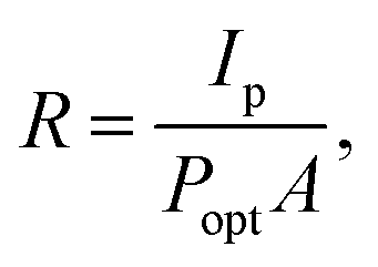
Responsivity is a significant index to assess the performance of UV detectors. The responsivity of a detector, R, is defined as
The photocurrent time response of the device was measured at 0 V bias under an intermittent irradiation of a 365 nm UV LED with a power of 60 μW cm−2 and four repeated cycles are plotted in Fig. 3(d). A short photoresponse time (∼0.1 s) in our device is observed. However, the photocurrent shows a slightly decrease after bending, while it reverts to the original level after the removal of bending force. It is the Schottky contact between ZnO and water which principally enables the device to run. And we will discuss the principle of device in detail later. It is believed that both the surface of the ZnO seed layer and ZnO NWs which are exposed to the water contribute to the photocurrent. Typically, the ZnO NWs contribute to the photocurrent more in the system due to its larger surface area. As is well known, the piezoelectric polarization fields of w-ZnO is along the c-axis and the ZnO seed layer we deposited in this work is grown along the c-axis. Thus, we think the decrease of photocurrent is caused by the piezoelectric polarization when applying the tensile strain to the device. Positive piezoelectric polarization charges are induced in the vicinity of ZnO/H2O interface and thus attract free electrons which will decrease the barrier height, leading to the weakening of the built-in electric field. So that the efficiency of separation of electron–hole pairs drops, which results in a reduced photocurrent.35 Overall, in spite of the slight difference in the value of photocurrent, the performance of our device keeps stable in different testing conditions, which is very important to flexible UV detector.
To further enhance the performance of obtained device, we decorated the ZnO NWs with Ag nanoparticles. To better study the forming mechanism of the Ag nanoparticles deposited on ZnO NWs, concentration-dependent morphology evolution experiments were performed. The SEM images of two ZnO NWs samples which were immersed in the aqueous solution with different Ag+ ions concentration (0.001 and 0.01 mM) are illustrated in Fig. 4(a and b). As shown in Fig. 4, it is observed that the size of Ag nanoparticle becomes larger with the increase of Ag+ ions concentration. Under the lower concentration of Ag+ ions (1 μM), the nanoparticles tend to form tiny beaded granules with the diameter of ∼30 nm, as illustrated in Fig. 4(a). Interestingly, flake-like structures are formed when the concentration of Ag+ ions increases to 10 μM, and the sizes of which are commonly beyond 500 nm (Fig. 3(b)). To confirm the formation of Ag nanoparticles, the structures were further investigated by EDX analysis. In Fig. 5(a and b), it is obviously observed that the nanoparticles are uniformly attached on the ZnO NWs. EDX mapping information (Fig. 5(c–e)) was collected by scanning the whole area of the samples, as shown in Fig. 5(a). Fig. 5(c–e) correspond to the distribution of the elements of Zn, O, Ag, respectively, confirming the uniform deposition of Ag particles onto the ZnO NWs. Seen from the TEM image of a single ZnO NW in Fig. 6(a), a nanoparticle is found on the surface of single ZnO NW. To verify whether the particle is Ag particle, a line scanning (the red line in Fig. 6(b)) was performed across the particle by EDX spectrometer equipped on TEM. TEM results (Fig. 6(c–d)) give the distribution of the Ag element across the whole scanning line, which proves that the nanoparticles attached to the ZnO NWs are Ag nanoparticles. A simple proposed mechanism to explain the formation of Ag nanoparticles is discussed. Firstly, the Ag+ ions were adsorbed on the surface of ZnO NWs. Afterwards, when the UV rays irradiated on the ZnO NWs, the electrons were generated in the conduction band of ZnO by absorbing the energy of UV light. The generated electrons were captured by the Ag+ ions, reducing which into Ag nanoparticles.36 It is easy to assume that the density of Ag+ adsorbed on the surface of ZnO NWs is proportional to Ag+ ions concentration. The overcrowded Ag+ ions may either reunite together to form greater nanoparticles under the UV light or merge into the Ag-slices after being reduced into Ag nanoparticles if the distance between every two emerging particles is short enough, namely, shorter than the diameter of the particle.
 | ||
| Fig. 4 (a) Tilt-view SEM image of ZnO NWs modified by 1 μM AgNO3 solution; (b) top-view SEM image of ZnO NWs modified by 10 μM AgNO3 solution. | ||
 | ||
| Fig. 5 (a) Top-view SEM image of ZnO NWs modified by 1 μM AgNO3 solution; (b) cross-sectional image of ZnO NWs modified by 1 μM AgNO3 solution; (c–e) EDX images of each element in the whole area showed in (a). | ||
 | ||
| Fig. 6 (a) Low-magnification TEM image of a single ZnO NW; (b) linear scanning image of (a), red line is the scanning line; (c and d) the distribution of the Ag element across the scanning line shown in (b). | ||
Typical I–V characteristics curves of the two Ag nanoparticles-modified detectors are illustrated in Fig. 7(a and b), respectively. The relevant data are recorded in Table 1. As shown in Fig. 7(a), a clear gap between the photocurrent line and dark current line is observed at 0 V bias voltage, signifying a good sensitivity of the device (sample 2). However, such obvious distinction is hard to be observed in Fig. 7(b) (sample 3). Table 1 also shows that the responsivity falls when the concentration of Ag+ increases to 10 μM. The photocurrent time response curves are plotted in Fig. 8, illustrating that the performance of device has been enhanced by the modification with the Ag nanoparticles with the size of ∼30 nm while weakened with the size of 500 nm. The sharp peaks shown in the Fig. 8 may be related to the poor charge transport at the semiconductor and liquid interface. The accumulated charges at the interface induce a large recombination current, corresponding to the sharp peak. The phenomenon resembles the charging and discharging process of a capacitor. Such phenomenon is more obvious in sample 2. We speculate that the Ag nanoparticles may help the accumulation of the charges, resulting in a larger recombination current. As discussed in the last section, the size of Ag nanoparticles differs a lot due to the distinct difference between the concentrations of the Ag+ ions in the solution. Considering the different performance of device by the modification with the Ag nanoparticles, it is believed that Ag nanoparticles with different sizes grown on the semiconductors interact distinctively with incident light. As depicted in the Fig. 9, in the UV-A region, the intensity of absorption has boosted when modified by the 1 μM AgNO3 solution and reduced when modified by the 10 μM AgNO3 solution, which is consistent with the results of responsivity. It is believed that the enhancement of the absorption arises from the LSPR effect. The strong local field enhancement in the vicinity of the noble metal nanoparticles increases absorption in a surrounding semiconductor material, and the Ag nanoparticles act as an effective subwavelength antenna for the incident light, which collects the incident energy in a localized surface plasmon mode. However, when the size of Ag particles is much larger than the diameter of ZnO NWs, the Ag flake-like structures work as a blocking layer to prevent ZnO NWs from absorbing UV light. Thereby the decrease of absorption displayed in Fig. 9 (green line graph) can be explained. The connection between the intensity of absorption and the size of particles is profound and complicated, nevertheless, we believe that the Ag nanoparticles with the diameter of ∼30 nm are capable of interacting with the incident light through the oscillations of conduction electrons so as to concentrate the electromagnetic waves within the near-field regions (<100 nm) close to their surfaces. Since the average width of the gaps among the ZnO NW arrays is within 100 nm, the gaps lie in the near-field regions described above, where the whole beam of light may penetrate freely if without the interactive effect of Ag nanoparticles. Therefore, the utilization of the incident light is enhanced in a sense. Above all, it is concluded that the Ag nanoparticles with certain sizes can enhance the absorption of light while Ag particles with large sizes (>500 nm) decrease the absorption of light inversely. However, more explicit and in-depth research should be done in the future to further unveil the connections between the size of Ag particles and the absorption of light.
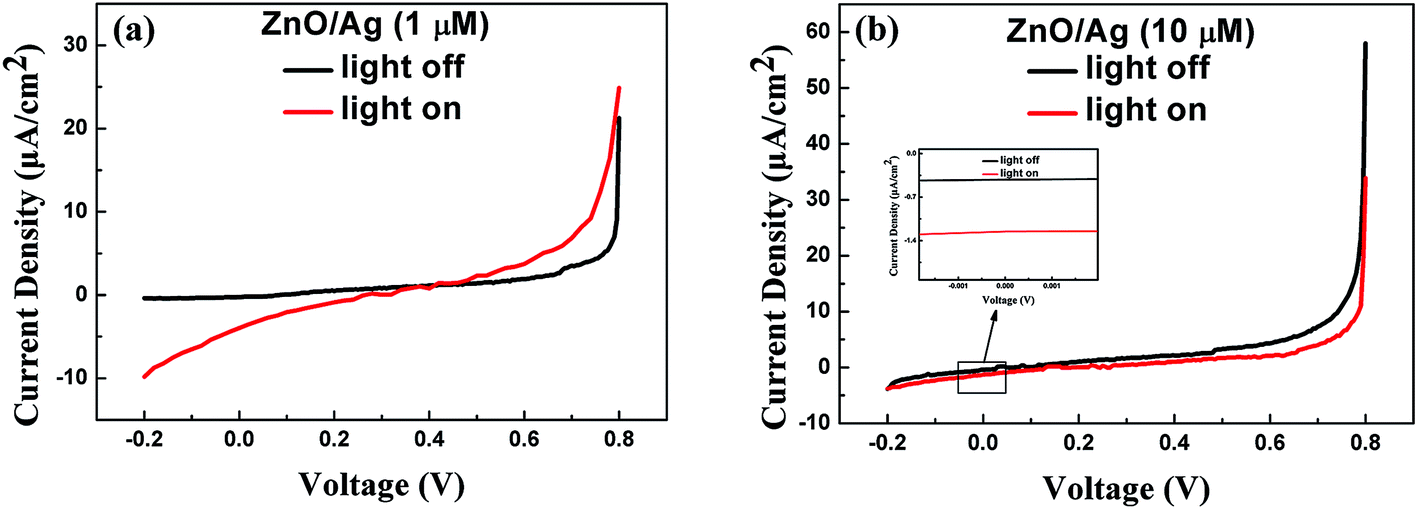 | ||
| Fig. 7 (a) I–V characteristics of Ag nanoparticles-modified ZnO NWs based detector (sample 2) in darkness and under the illumination of 60 μW cm−2 of UV light (λ = 365 nm); (b) I–V characteristics of Ag nanoparticles-modified ZnO NWs based detector (sample 3) in darkness and under the illumination of 60 μW cm−2 of UV light (λ = 365 nm), the inset is the zoomed-up figure of the selected area. | ||
 | ||
| Fig. 8 Photocurrent response of the three samples (sample 1, sample 2 and sample 3) under on/off radiation of 60 μW cm−2 of UV light (λ = 365 nm). | ||
 | ||
| Fig. 9 UV-visible light absorption spectra of ZnO NWs and Ag nanoparticles-modified ZnO NWs prepared at different AgNO3 concentrations. | ||
A simple functioning mechanism of our device is discussed. In brief, a built-in electric field is formed due to the difference of the Fermi level of ZnO and water. Therefore, after absorbing the energy of the UV light, the electron–hole pairs are generated and automatically separated by the electric force. Separated electrons travel along the ZnO NWs and transfer to the counter-electrode while the holes drift to the water side. A circular reaction is happening in the device. Holes oxidize the OH− ion to OH˙ radical, simultaneously, OH˙ radical is reduced to OH− ion by acquiring the negative electron with the help of Pt catalyst. In this process, the device is working continuously without external applied energy as long as the appropriate UV light at certain wavelength maintained illumination.
Conclusion
In conclusion, the ZnO NWs were grown vertically on the ITO coated PET substrate by a modified hydrothermal method. The flexible PECC type self-powered UV detectors was first fabricated and perform normally whenever in flat or bending status, showing strong potential in the wearable and flexible electronic applications. However, the responsivity is low compared to the non-plastic devices. Inspired by the LSPR effect, we have modified our devices by depositing certain sized Ag nanoparticles on the ZnO NWs and improved the performance of our devices. Considering that it is difficult to improve the crystal quality of ZnO NWs grown on the flexible substrates at low temperature, it is a good guide for us to enhance the performance of flexible UV detectors. The fabrication of flexible self-powered UV detectors represents a significant step toward future multifunctional optoelectronic applications.Acknowledgements
This work was supported by National Natural Science Foundation of China under Grant No. 51302244 and 91333203, and the Fundamental Research Funds for the Central Universities under Grant No. 2015FZA4007.References
- M. Razeghi and A. Rogalski, J. Appl. Phys., 1996, 79, 7433 CrossRef CAS.
- K. Liu, M. Sakurai and M. Aono, Sensors, 2010, 10, 8604–8634 CrossRef CAS PubMed.
- E. Monroy, F. Calle, J. L. Pau, E. Muñoz, F. Omnès, B. Beaumont and P. Gibart, J. Cryst. Growth, 2001, 230, 537–543 CrossRef CAS.
- E. Muñoz, E. Monroy, J. L. Pau, F. Omnès and P. Gibart, J. Phys.: Condens. Matter, 2001, 13, 7115–7137 CrossRef.
- A. B. Djurišić and Y. H. Leung, Small, 2006, 2, 944–961 CrossRef PubMed.
- C. Klingshirn, Phys. Status Solidi B, 2007, 244, 3027–3073 CrossRef CAS.
- U. Özgür, Y. I. Alivov, C. Liu, A. Teke, M. A. Reshchikov, S. Doğan, V. Avrutin, S. J. Cho and H. Morkoç, J. Appl. Phys., 2005, 98, 41301 CrossRef.
- A. S. Aricò and B. S. Peter Bruce, Nat. Mater., 2005, 4, 366–377 CrossRef PubMed.
- K. J. Chen, F. Y. Hung, S. J. Chang and S. J. Young, J. Alloys Compd., 2009, 479, 674–677 CrossRef CAS.
- Z. R. Tian, J. A. Voigt, J. Liu, B. Mckenzie, M. J. Mcdermott, M. A. Rodriguez, H. Konishi and H. Xu, Nat. Mater., 2003, 2, 821–826 CrossRef CAS PubMed.
- Y. Zhang, X. Wang, Y. Wu, J. Jie, X. Zhang, Y. Xing, H. Wu, B. Zou, X. Zhang and X. Zhang, J. Mater. Chem., 2012, 22, 14357 RSC.
- J. M. Wu, Y. Chen and Y. Lin, Nanoscale, 2011, 3, 1053–1058 RSC.
- J. B. K. Law and J. T. L. Thong, Appl. Phys. Lett., 2006, 88, 133114 CrossRef.
- H. Y. B. M. Hannes Kind and A. P. Y. Matthew Law, Adv. Mater., 2002, 14, 158–160 CrossRef.
- S. Bai, W. Wu, Y. Qin, N. Cui, D. J. Bayerl and X. Wang, Adv. Funct. Mater., 2011, 21, 4464–4469 CrossRef CAS.
- Q. A. Xu, J. W. Zhang, K. R. Ju, X. D. Yang and X. Hou, J. Cryst. Growth, 2006, 289, 44–47 CrossRef CAS.
- K. W. Liu, J. G. Ma, J. Y. Zhang, Y. M. Lu, D. Y. Jiang, B. H. Li, D. X. Zhao, Z. Z. Zhang, B. Yao and D. Z. Shen, Solid-State Electron., 2007, 51, 757–761 CrossRef CAS.
- X. G. Zheng, Q. S. Li, J. P. Zhao, D. Chen, B. Zhao, Y. J. Yang and L. C. Zhang, Appl. Surf. Sci., 2006, 253, 2264–2267 CrossRef CAS.
- K. Wang, Y. Vygranenko and A. Nathan, J. Appl. Phys., 2007, 101, 114508 CrossRef.
- W. Dai, X. Pan, S. Chen, C. Chen, Z. Wen, H. Zhang and Z. Ye, J. Mater. Chem. C, 2014, 2, 4606 RSC.
- C. Chen, S. Chang, S. Chang, M. Li, I. Chen, T. Hsueh and C. Hsu, Chem. Phys. Lett., 2009, 476, 69–72 CrossRef CAS.
- H. S. Y. L. S. Lianga, J. Cryst. Growth, 2001, 225, 110–113 CrossRef.
- Y. Zeng, X. Pan, W. Dai, Y. Chen and Z. Ye, RSC Adv., 2015, 5, 66738–66741 RSC.
- Y. Xie, L. Wei, Q. Li, Y. Chen, S. Yan, J. Jiao, G. Liu and L. Mei, Nanotechnology, 2014, 25, 75202 CrossRef PubMed.
- Y. Xie, L. Wei, G. Wei, Q. Li, D. Wang, Y. Chen, S. Yan, G. Liu, L. Mei and J. Jiao, Nanoscale Res. Lett., 2013, 8, 188 CrossRef PubMed.
- O. Game, U. Singh, T. Kumari, A. Banpurkar and S. Ogale, Nanoscale, 2014, 6, 503–513 RSC.
- W. Lee and M. Hon, Appl. Phys. Lett., 2011, 99, 251102 CrossRef.
- P. Lin, X. Yan, Y. Liu, P. Li, S. Lu and Y. Zhang, Phys. Chem. Chem. Phys., 2014, 16, 26697–26700 RSC.
- K. Liu, M. Sakurai, M. Liao and M. Aono, J. Phys. Chem. C, 2010, 114, 19835–19839 CAS.
- A. Rajan, H. K. Yadav, V. Gupta and M. Tomar, Appl. Phys. A, 2014, 116, 913–919 CrossRef CAS.
- R. A. Naphade, M. Tathavadekar, J. P. Jog, S. Agarkar and S. Ogale, J. Mater. Chem. A, 2014, 2, 975–984 CAS.
- A. Polman, Science, 2008, 322, 868–869 CrossRef PubMed.
- H. A. Atwater and A. Polman, Nat. Mater., 2010, 9, 205–213 CrossRef CAS PubMed.
- S. M. P. L. W. Ji, Appl. Phys. Lett., 2009, 94, 203106 CrossRef.
- K. C. Pradel, W. Wu, Y. Zhou, X. Wen, Y. Ding and Z. L. Wang, Nano Lett., 2013, 13, 2647–2653 CrossRef CAS PubMed.
- T. Wang, Z. Jiao, T. Chen, Y. Li, W. Ren, S. Lin, G. Lu, J. Ye and Y. Bi, Nanoscale, 2013, 5, 7552 RSC.
| This journal is © The Royal Society of Chemistry 2016 |