
 Open Access Article
 This Open Access Article is licensed under a
 Creative Commons Attribution 3.0 Unported Licence
Self-assembly and charge carrier transport of solution-processed conjugated polymer monolayers on dielectric surfaces with controlled sub-nanometer roughness†
Mengmeng
Li
a,
Felix
Hinkel
a,
Klaus
Müllen
*a and
Wojciech
Pisula
*ab
aMax Planck Institute for Polymer Research, Ackermannweg 10, 55128 Mainz, Germany. E-mail: pisula@mpip-mainz.mpg.de; muellen@mpip-mainz.mpg.de
bDepartment of Molecular Physics, Faculty of Chemistry, Lodz University of Technology, Zeromskiego 116, 90-924 Lodz, Poland
First published on 30th March 2016
Abstract
In recent years organic field-effect transistors have received extensive attention, however, it is still a great challenge to fabricate monolayer-based devices of conjugated polymers. In this study, one single layer of poly(2,5-bis(3-alkylthiophen-2-yl)thieno[3,2-b]thiophene) is directly dip-coated, and its self-assembly is precisely tuned from nanofibers to granular aggregates by controlling the dielectric roughness on a sub-nanometer scale. The charge carrier transport of the monolayer transistor exhibits a strong dependence on the dielectric roughness, which is attributed to the roughness-induced effects of higher densities of grain boundaries and charge trapping sites as well as surface scattering. These results mark a great advance in the bottom-up fabrication of organic electronics.
Introduction
In the past two decades, tremendous progress has been made in both organic semiconducting materials and device engineering for organic field-effect transistors (OFETs). So far it has been widely proven and accepted that the first few layers near the dielectric are primarily responsible for the charge carrier transport in OFETs.1 Recent studies on small molecules have already realized the bottom-up fabrication of monolayer transistors in which a single molecular layer is sufficient as the semiconducting channel.2–6 In particular, a monolayer of 1,4-bis((5′-hexyl-2,2′-bithiophen-5-yl)ethynyl)benzene was grown in the formation of two dimensional single crystals by drop-casting, and an excellent charge carrier transport was reported with the mobility up to 1 cm2 V−1 s−1.6 Such monolayer transistors could bear great potential in the near future due to their unique advantages such as lower cost, higher sensitivity and transparency.7 However, in comparison with their small molecule counterparts, it is still a great challenge to fabricate operating OFET devices using a single layer of conjugated polymers as a semiconducting channel. The Langmuir–Blodgett (LB) technique is an alternative approach for the fabrication of conjugated polymer monolayers,8 however, it has to be noted that a water base is generally utilized during LB processing, which causes charge trapping and has a detrimental influence on the charge carrier transport in OFET devices.9The surface properties of the dielectric, including chemical composition, surface energy, surface viscoelasticity, and especially surface roughness critically affect the semiconductor film microstructure and charge carrier transport in OFETs.10–13 Early studies demonstrated that the charge carrier mobility of pentacene thin films (50 nm) was strongly dependent on the dielectric roughness, which could be explained by the “roughness valley” theory.14 It was also reported that a dielectric root-mean square roughness (Rms) greater than 0.5 nm severely inhibited the molecular order of poly(2,5-bis(3-alkylthiophen-2-yl)thieno[3,2-b]thiophene) (PBTTT, ∼20 nm) so that the charge carrier mobility was significantly reduced.15 In spite of these findings, the precise control of the self-assembly and charge carrier transport of conjugated polymer monolayer transistors has not yet been achieved.
Previously, we proposed an effective solution method to precisely tune the Rms value of the SiO2 surface on a sub-nanometer scale by which the intrinsic role of the interfacial order of organic semiconductors on the charge carrier transport was successfully revealed.16 In the present study, a donor–acceptor copolymer, poly[2,6-(4,4-bis(2-ethylhexyl)-4H-cyclopenta[2,1-b:3,4-b′]-dithiophene)-alt-4,7-(2,1,3-benzothiadiazole)] (PCPDTBT, Fig. 1), is processed into a monolayer by dip-coating which is a known technique to deposit organic semiconductors in a well-defined manner.17–19 Dielectrics with sub-nanometer roughness (S1–S4) are employed to kinetically control the self-assembly of this conjugated polymer monolayer. It is found that a high Rms induces an obvious energy barrier for the polymer chain mobility, so that long-range ordering is severely disrupted. Moreover, the charge carrier transport exhibits a roughness-dependent behavior, and the hole mobility is dramatically decreased from 5.08 ± 0.67 × 10⁻⁴ to 1.01 ± 0.22 × 10⁻⁴ cm2 V−1 s−1 with increasing Rms from 0.19 to 0.39 nm. Therefore, with the assistance of the sub-nanometer dielectric roughness, the precise control of a conjugated polymer monolayer is successfully achieved from both aspects of self-assembly and charge carrier transport.
 | ||
| Fig. 1 Schematic illustration of the device configuration. The top is the chemical structure of PCPDTBT, and the bottom is the sub-nanoscale dielectric roughness. | ||
Results and discussion
The deposition of PCPDTBT ultrathin films can be controlled in a monolayer precision by dip-coating from a 0.5 mg mL−1 chloroform solution. With a pulling speed of 400 μm s−1, a single polymer layer is fabricated on a silicon substrate (with 300 nm-thick thermally grown SiO2), and the morphology is characterized by tapping-mode atomic force microscopy (AFM), as shown in Fig. 2a and b. It is evident from Fig. 2c that the monolayer thickness is ∼2 nm. This value is in good agreement with the interlayer distance of this copolymer as measured by X-ray scattering,20a so that it can be assumed that the polymer backbone is arranged edge-on towards the surface. It has to be noted that this monolayer consists of oval-shaped nanofibers. For PCPDTBT, π-stacking forces occur parallel to the width, and the weaker alkyl interactions along the fiber height leading to oval shaped fibers.20b The phase image in Fig. 2b shows that the dark section represents the polymer nanofibers and the bright one corresponds to the uncovered substrate. Moreover, the number of polymer layers (N) is strongly dependent on the pulling speed (U). Five different pulling speeds are utilized: 1000, 400, 100, 50, and 20 μm s−1, respectively. By continuously decreasing U from 1000 to 20 μm s−1, the first two layers were nearly fully covered on the substrate, accompanied by the deposition of the third and fourth layers (Fig. 2d and S1†). As a result, the optimized pulling speed of U = 400 μm s−1 is used to fabricate PCPDTBT monolayers.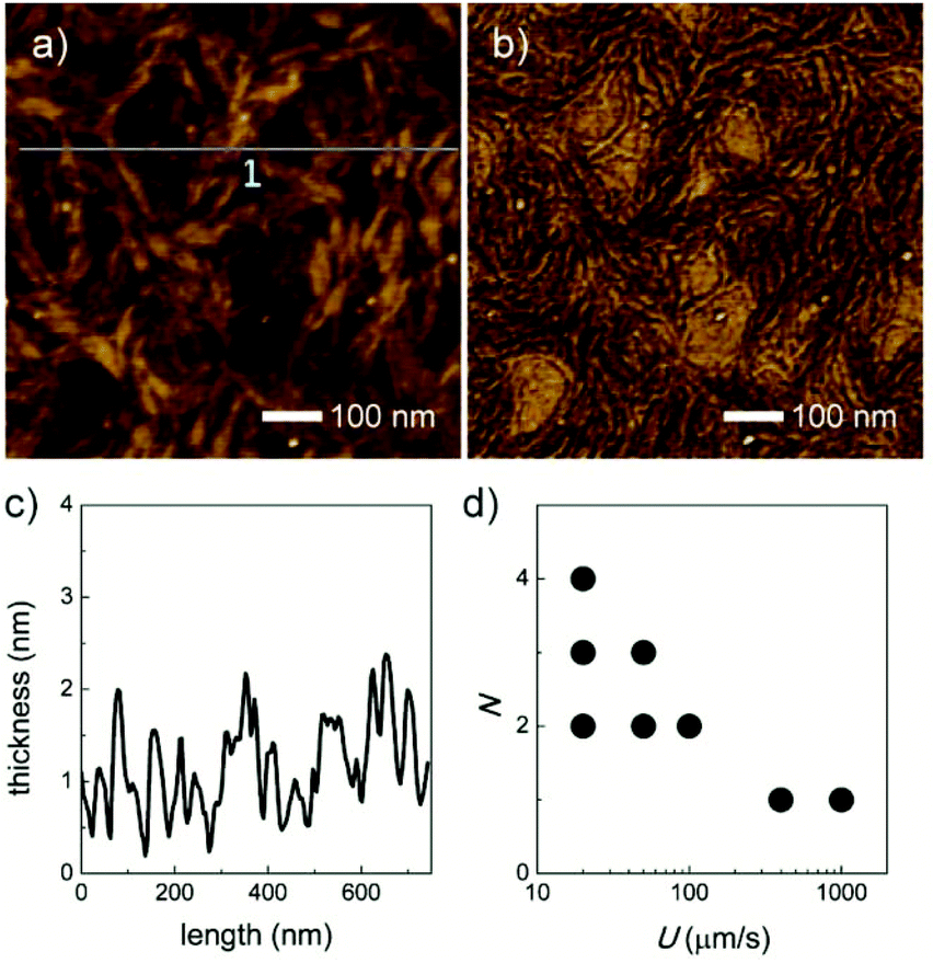 | ||
| Fig. 2 AFM height (a) and phase (b) images of the PCPDTBT monolayer dip-coated with a speed of 400 μm s−1 on a silicon substrate (with 300 nm-thick thermally grown SiO2). (c) The corresponding height plots in (a). (d) Evolution of the number of molecular layers (N) with pulling speed (U) (multiple dots indicate population of several layer thicknesses in the same film). | ||
The dielectric roughness plays a critical role in the microstructure of organic semiconducting layers. Most previous studies reported the use of dielectrics with a roughness in the nanometer range by which the molecular order was severely destroyed in the entire film.14,15 In contrast, we found that roughness within a sub-nanometer scale allows the precise tuning of the self-assembly of organic semiconductors in monolayers.16 This sub-nanometer roughness is obtained by spin-coating a hydrolyzed tetramethyl orthosilicate (TMOS) solution on silicon wafers. This spin-coated layer is annealed at high temperature resulting in the formation of a 10 nm-thick SiO2 layer on the silicon wafer. The preparation details are described in the Experimental section. In comparison with a native oxide layer of the commercial silicon wafer (300 nm), the capacity change due to the slight thickness increase (∼10 nm) can be neglected. In this way, the dielectric roughness can be precisely modified from Rms = 0.19 to Rms = 0.39 nm (S1–S4, Table S1†). The Rms of the bare SiO2 substrate is ∼0.2 nm that is similar to the value of S1. It has been already proven that the conjugated polymer deposited on the bare SiO2 substrate exhibited an identical morphology and device performance to the one on S1.16
S1 has the smoothest surface with a Rms value of 0.19 nm, which is a little smaller than that of the commercial silicon wafer (∼0.2 nm). As determined by AFM, the PCPDTBT monolayer deposited on S1 is also composed of nanofibers with a 10 nm diameter which is identical to that on the silicon wafer (Fig. 2a, b and 3a, e). The charge carrier transport of the PCPDTBT monolayer is quantitatively evaluated by fabricating OFET devices. A top-contact bottom-gate configuration is employed based on the following considerations (Fig. 1). Firstly, top-contact transistors usually show a higher mobility than devices with a bottom-contact architecture,20c,d and this difference is even more pronounced for ultrathin films.20e The higher contact resistance in the bottom-contact device is attributed to a lower contact area between source/drain (S/D) electrodes and the semiconductor layer.20f Secondly, the bottom-contact transistor often leads to a poor morphology around the S/D electrodes bearing a detrimental influence on the charge carrier transport.20f The device fabrication is described in detail in the Experimental section. Before OFET measurement, the PCPDTBT monolayer is annealed at 120 °C for 30 min to remove the residual solvent. This posttreatment rarely has an influence on the microstructure of the deposited polymer monolayers.16 On the other hand, the specific transfer and output plots of the polymer monolayer on S1 exhibit a typical linear/saturation behavior, as shown in Fig. 4a and e. At a gate voltage (VGS) of −80 V, the drain current (−IDS) reaches 0.2 μA. The saturation mobility in holes (μh) of this monolayer transistor is 5.08 ± 0.67 × 10⁻⁴ cm2 V−1 s−1, with the maximum value of 6.42 × 10⁻⁴ cm2 V−1 s−1. It is worth pointing out that no field-effect characteristics were observed for the single layer of organic semiconductors in many cases.17,18,21 In addition, it must be emphasized that this μh value is not optimized and is underestimated because (i) no special surface treatment for the dielectric is applied, such as the use of self-assembled monolayers (SAMs) to reduce the trapping sites for charge carriers; (ii) the mobility extraction from transfer plots is carried out for a fully covered monolayer which is not the case for S1. The on/off ratio of the monolayer on S1 is around 103.
 | ||
| Fig. 3 (a–d) AFM height images of the PCPDTBT monolayer dip-coated on substrates S1–S4. The monolayer thickness is 2.4, 2.8, 3.1, and 3.4 nm for S1–S4, respectively. (e–h) The corresponding phase images of (a–d). The scale bar corresponds to 200 nm in all images. | ||
 | ||
| Fig. 4 (a–d) Transfer curves of PCPDTBT monolayers dip-coated on S1–S4 and (e–h) are the corresponding output curves. In the transfer plots a source–drain voltage (VDS) of −80 V is applied. | ||
Increasing Rms to 0.27 nm (S2) does not lead to a significant change in the morphology. The nanofiber based monolayer is still obvious, as determined by the AFM height and phase images (Fig. 3b and f). The monolayer on S2 exhibits a hole mobility of 3.65 ± 0.13 × 10⁻⁴ cm2 V−1 s−1 and an on/off ratio of 102–103 (Fig. 4b and f). In comparison with the monolayer on S1, the μh value is reduced by 28%, which can be attributed to two aspects. Firstly, more trapping sites are induced by a higher Rms so that the charge carrier transport is decreased. Secondly, the surface scattering on charge carriers is intensified, hindering the movement of charge carriers along the working channel.14,22 With a further increase in the dielectric roughness to 0.30 nm (S3), the chain mobility of the conjugated polymer is continuously decreased, which results in a lower propensity to self-assemble (Fig. 3c and g). Consequently, the hole transport of the PCPDTBT monolayer gradually deteriorates with a charge carrier mobility of 3.40 ± 0.59 × 10⁻⁴ cm2 V−1 s−1 (Fig. 4c and g). The output characteristics in Fig. 4f and g reveal a nonlinear behavior of IDS at a low VDS indicating contact resistance and charge injection limitation.23,24
When a dielectric with a higher Rms value (S4) is utilized to deposit the PCPDTBT monolayer, the long-range ordering of PCPDTBT is significantly hindered, with a transition of the polymer self-assembly from an ordered (nanofibers) to a disordered microstructure (granular aggregates) (Fig. 3d and h). This transition originates from the insufficient chain mobility of the conjugated polymer which cannot overcome the roughness-induced barrier and is hampered in the self-organization into nanofibers.25 The monolayer on S4 reveals not only a much poorer organization, but also more grain boundaries resulting in a low μh value of 1.01 ± 0.22 × 10⁻⁴ cm2 V−1 s−1. This decline in hole mobility correlates well with the decrease in −IDS by approximately one order of magnitude from 0.2 to 0.03 μA (Fig. 4d and h). Furthermore, the transfer curve at a low VGS exhibits a more obvious trapping effect as well as a higher turn-on voltage. In addition, both transfer and output characteristics of the monolayer on S4 indicate a stronger effect of contact resistance and charge injection limitation.17
The roughness-dependent behavior of the charge carrier mobility is summarized in Fig. 5a. It can be clearly seen that the hole mobility is reduced with increasing the value of Rms, which is in good agreement with the reported “roughness valley” theory.14 Besides the increased density of charge trapping and surface scattering induced by a higher Rms, the molecular order is another factor responsible for the 5-fold decline in the charge carrier transport, as shown in Fig. 5b. In contrast to the highly organized monolayer on a smooth dielectric such as S1, the molecular self-assembly is severely inhibited by the roughness-induced barrier (S4). This leads to a poor molecular ordering and more grain boundaries, and finally as a consequence hinders the transport of charge carriers. It is worth noting that the decrease in mobility is less than one order of magnitude in spite of significant changes in the film microstructure. This is reasonable because the long polymer chains are effective to bridge the ordered domains providing sufficient pathways for charge carriers.26,27 Additionally, the bridging effect of polymer chains may contribute to the unchanged on/off ratio and threshold voltage, as shown in Table S3.†26,27
 | ||
| Fig. 5 (a) Relationship between hole mobility and dielectric roughness. (b) Illustration of the molecular order on smooth (S1) and rough (S4) dielectrics. | ||
Conclusions
In conclusion, the self-assembly of conjugated polymer monolayers is kinetically tuned by controlling the dielectric roughness on the sub-nanometer scale. It has been revealed that a higher Rms significantly inhibits the molecular organization in the monolayer leading to a change in the microstructure from well-defined nanofibers to small aggregates. At the same time, the hole mobility of the monolayer transistor has an obvious reduction from 5.08 ± 0.67 × 10⁻⁴ to 1.01 ± 0.22 × 10⁻⁴ cm2 V−1 s−1 with increasing Rms from 0.19 to 0.39 nm. This roughness-dependent mobility is attributed to increased trapping sites, surface scattering of charge carriers, and a poor molecular order.Therefore, the precise control over the self-assembly and charge carrier transport of conjugated polymer monolayers is successfully achieved with the assistance of the sub-nanometer dielectric roughness. It is still a big challenge to fabricate working transistors based on a polymer monolayer.17,18,21 In spite of the hole mobility of 10−4 cm2 V−1 s−1 in this study, these results mark a great advance in the bottom-up fabrication of organic electronics, especially for conjugated polymers. Most importantly, this study provides further evidence for the possibility of kinetically controlling the self-assembly and charge carrier transport of conjugated polymer monolayers. Therefore, the sub-nanometer dielectric roughness prepared by our method can be considered as a promising tool for interfacial engineering in the field of organic electronics. In this way, the self-assembly and charge carrier transport in a monolayer can be precisely tuned.
Experimental section
General
PCPDTBT was synthesized using a general polymerization procedure according to a modified literature procedure.28 Further purification was employed by soxhlet-extraction with acetone, hexane and ethyl acetate. After precipitation from 1,2,4-trichlorobenzene (TCB) in methanol, the polymer was obtained as a dark solid. The high molecular weight of the polymer led to a broad polydispersity index (PDI) of 5 due to enhanced aggregation in GPC analysis (TCB). The molecular weight (Mn) of the polymer was thereby determined as 40 kg mol−1. Morphologies of the polymer monolayer were characterized by a Digital Instruments Nanoscope IIIa Atomic Force Microscope (AFM) in the tapping mode.Dielectrics with sub-nanometer surface roughness
The preparation of S1–S4 was described elsewhere.16 Briefly, 4 mL of TMOS solution in ethanol was prepared at a concentration of 0.5 mg mL−1 at 70 °C. Subsequently, 0.8 mL of HCl (40 mM) was mixed into the solution to hydrolyze TMOS. Afterwards, the solution was aged for 24 h. 1 mL of the aged solution was diluted by using a 9 mL of mixture of H2O and ethanol with a different volume ratio, and then mixed with a 10 mL of 2 mg mL−1 CTAB aqueous solution. The prepared precursor solutions were directly spin-coated onto the commercial wafers with a 300 nm-thick thermally grown silicon dioxide layer at a speed of 2000 rpm for 1 min. Finally, these spin-coated substrates were annealed at 700 °C for 1 h under a nitrogen atmosphere to remove organic impurities and obtain the silicon dioxide layer. The Rms value for each dielectric was calculated from 5–8 AFM images with a size of 2 × 2 μm2. Rms values of S1–S4 are summarized in Table S1.†Fabrication of conjugated polymer monolayer transistors
S1–S4 were cleaned by ultrasonication in acetone for 10 min, followed by ultrasonication in isopropanol for another 10 min. Then the monolayer was deposited by dip-coating from a 0.5 mg mL−1 PCPDTBT chloroform solution with a pulling speed of 400 μm s−1. The bottom-gate top-contact configuration was employed for OFET devices. The source and drain electrodes with a 60 nm thickness were deposited by Au evaporation. The channel length and width are 20 and 400 μm, respectively.Electrical characterization
Before measurement, annealing at 120 °C was applied for 30 min in order to remove residual solvents. A Keithley 4200-SCS was used for all standard electrical measurements in a glovebox under a nitrogen atmosphere. The average mobilites for polymer monolayer transistors on each dielectric were calculated from 3–7 devices.Acknowledgements
M. L. acknowledges financial support from the ERC-Adv.-Grant 267160 (NANOGRAPH).References
- F. Dinelli, M. Murgia, P. Levy, M. Cavallini, F. Biscarini and D. M. de Leeuw, Phys. Rev. Lett., 2004, 92, 116802 CrossRef PubMed.
- G. S. Tulevski, Q. Miao, M. Fukuto, R. Abram, B. Ocko, R. Pindak, M. L. Steigerwald, C. R. Kagan and C. Nuckolls, J. Am. Chem. Soc., 2004, 126, 15048–15050 CrossRef CAS PubMed.
- E. C. P. Smits, S. G. J. Mathijssen, P. A. van Hal, S. Setayesh, T. C. T. Geuns, K. A. H. A. Mutsaers, E. Cantatore, H. J. Wondergem, O. Werzer, R. Resel, M. Kemerink, S. Kirchmeyer, A. M. Muzafarov, S. A. Ponomarenko, B. de Boer, P. W. M. Blom and D. M. de Leeuw, Nature, 2008, 455, 956–959 CrossRef CAS.
- J. Huang, J. Sun and H. E. Katz, Adv. Mater., 2008, 20, 2567–2572 CrossRef CAS.
- S. G. J. Mathijssen, E. C. P. Smits, P. A. van Hal, H. J. Wondergem, S. A. Ponomarenko, A. Moser, R. Resel, P. A. Bobbert, M. Kemerink, R. A. J. Janssen and D. M. de Leeuw, Nat. Nanotechnol, 2009, 4, 674–680 CrossRef CAS PubMed.
- L. Jiang, H. Dong, Q. Meng, H. Li, M. He, Z. Wei, Y. He and W. Hu, Adv. Mater., 2011, 23, 2059–2063 CrossRef CAS PubMed.
- F. Zhang, C.-A. Di, N. Berdunov, Y. Hu, Y. Hu, X. Gao, Q. Meng, H. Sirringhaus and D. Zhu, Adv. Mater., 2013, 25, 1401–1407 CrossRef CAS PubMed.
- (a) J. C. Scott, J. D. J. Samuel, J. H. Hou, C. T. Rettner and R. D. Miller, Nano Lett., 2006, 6, 2916–2919 CrossRef CAS PubMed; (b) J. Paloheimo, P. Kuivalainen, H. Stubb, E. Vuorimaa and P. Yli-Lahti, Appl. Phys. Lett., 1990, 56, 1157–1159 CrossRef CAS; (c) H. G. O. Sandberg, G. L. Frey, M. N. Shkunov, H. Sirringhaus, R. H. Friend, M. M. Nielsen and C. Kumpf, Langmuir, 2002, 18, 10176–10182 CrossRef CAS; (d) G. Xu, Z. Bao and J. T. Groves, Langmuir, 2000, 16, 1834–1841 CrossRef CAS; (e) S. Fabiano, C. Musumeci, Z. Chen, A. Scandurra, H. Wang, Y.-L. Loo, A. Facchetti and B. Pignataro, Adv. Mater., 2012, 24, 951–956 CrossRef CAS PubMed; (f) S. Fabiano, H. Yoshida, Z. Chen, A. Facchetti and M. A. Loi, ACS Appl. Mater. Interfaces, 2013, 5, 4417–4422 CrossRef CAS PubMed.
- (a) C. M. Aguirre, P. L. Levesque, M. Paillet, F. Lapointe, B. C. St-Antoine, P. Desjardins and R. Martel, Adv. Mater., 2009, 21, 3087–3091 CrossRef CAS; (b) S. Hoshino, M. Yoshida, S. Uemura, T. Kodzasa, N. Takada, T. Kamata and K. Yase, J. Appl. Phys., 2004, 95, 5088–5093 CrossRef CAS; (c) W. Kim, A. Javey, O. Vermesh, Q. Wang, Y. Li and H. Dai, Nano Lett., 2003, 3, 193–198 CrossRef CAS.
- C. Kim, A. Facchetti and T. J. Marks, Science, 2007, 318, 76–80 CrossRef CAS PubMed.
- H.-G. Min, E. Seo, J. Lee, N. Park and H. S. Lee, Synth. Met., 2013, 163, 7–12 CrossRef CAS.
- C. Kim, A. Facchetti and T. J. Marks, Adv. Mater., 2007, 19, 2561–2566 CrossRef CAS.
- L. L. Chua, P. K. H. Ho, H. Sirringhaus and R. H. Friend, Adv. Mater., 2004, 16, 1609–1615 CrossRef CAS.
- S. Steudel, S. De Vusser, S. De Jonge, D. Janssen, S. Verlaak, J. Genoe and P. Heremans, Appl. Phys. Lett., 2004, 85, 4400–4402 CrossRef CAS.
- Y. Jung, R. J. Kline, D. A. Fischer, E. K. Lin, M. Heeney, I. McCulloch and D. M. DeLongchamp, Adv. Funct. Mater., 2008, 18, 742–750 CrossRef CAS.
- M. Li, C. An, T. Marszalek, M. Baumgarten, K. Müllen and W. Pisula, Adv. Mater., 2016, 28, 2245–2252 CrossRef CAS PubMed.
- S. Wang, A. Kiersnowski, W. Pisula and K. Müllen, J. Am. Chem. Soc., 2012, 134, 4015–4018 CrossRef CAS PubMed.
- L. Li, P. Gao, K. C. Schuermann, S. Ostendorp, W. Wang, C. Du, Y. Lei, H. Fuchs, L. D. Cola, K. Müllen and L. Chi, J. Am. Chem. Soc., 2010, 132, 8807–8809 CrossRef CAS PubMed.
- L. Li, P. Gao, W. Wang, K. Müllen, H. Fuchs and L. Chi, Angew. Chem., Int. Ed., 2013, 52, 12530–12535 CrossRef CAS PubMed.
- (a) W. Pisula, H. N. Tsao, D. Dudenko, D. M. Cho, S. R. Puniredd, Y. Zhao, A. Mavrinskiy, J. Shu, M. R. Hansen, M. Baumgarten and K. Müllen, Polymers, 2013, 5, 833–846 CrossRef; (b) S. Wang, M. Kappl, I. Liebewirth, M. Müller, K. Kirchhoff, W. Pisula and K. Müllen, Adv. Mater., 2012, 24, 417–420 CrossRef CAS PubMed; (c) M. Mamada, J.-I Nishida, D. Kumaki, S. Tokito and Y. Yamashita, Chem. Mater., 2007, 19, 5404–5409 CrossRef CAS; (d) G. R. Dholakia, M. Meyyappan, A. Facchetti and T. J. Marks, Nano Lett., 2006, 6, 2447–2455 CrossRef CAS PubMed; (e) P. V. Pesavento, K. P. Puntambekar, C. D. Frisbie, J. C. McKeen and P. P. Ruden, J. Appl. Phys., 2006, 99, 094504 CrossRef; (f) D. Gupta, M. Katiyar and D. Gupta, Org. Electron., 2009, 10, 775–784 CrossRef CAS.
- S. Wang, W. Pisula and K. Müllen, J. Mater. Chem., 2012, 22, 24827–24831 RSC.
- A. R. Völkel, R. A. Street and D. Knipp, Phys. Rev. B: Condens. Matter, 2002, 66, 195336 CrossRef.
- W. Zhang, J. Smith, S. E. Watkins, R. Gysel, M. McGehee, A. Salleo, J. Kirkpatrick, S. Ashraf, T. Anthopoulos, M. Heeney and I. McCulloch, J. Am. Chem. Soc., 2010, 132, 11437–11439 CrossRef CAS PubMed.
- M. Caironi, C. Newman, J. R. Moore, D. Natali, H. Yan, A. Facchetti and H. Sirringhaus, Appl. Phys. Lett., 2010, 96, 183303 CrossRef.
- S. Kundu, R. Ganesan, N. Gaur, M. S. M. Saifullah, H. Hussain, H. Yang and C. S. Bhatia, Sci. Rep., 2012, 2 Search PubMed.
- R. Noriega, J. Rivnay, K. Vandewal, F. P. V. Koch, N. Stingelin, P. Smith, M. F. Toney and A. Salleo, Nat. Mater., 2013, 12, 1038–1044 CrossRef CAS PubMed.
- R. J. Kline, M. D. McGehee, E. N. Kadnikova, J. Liu, J. M. J. Fréchet and M. F. Toney, Macromolecules, 2005, 38, 3312–3319 CrossRef CAS.
- M. Zhang, H. N. Tsao, W. Pisula, C. Yang, A. K. Mishra and K. Müllen, J. Am. Chem. Soc., 2007, 129, 3472–3473 CrossRef CAS PubMed.
Footnote |
| † Electronic supplementary information (ESI) available. See DOI: 10.1039/c6nr01082b |
| This journal is © The Royal Society of Chemistry 2016 |