
 Open Access Article
 This Open Access Article is licensed under a
 Creative Commons Attribution 3.0 Unported Licence
Morphology analysis of near IR sensitized polymer/fullerene organic solar cells by implementing low bandgap heteroanalogue C-/Si-PCPDTBT†
Tayebeh
Ameri
*a,
Parisa
Khoram
a,
Thomas
Heumüller
a,
Derya
Baran
a,
Florian
Machui
a,
Anna
Troeger
c,
Vito
Sgobba
c,
Dirk M.
Guldi
c,
Marcus
Halik
d,
Silke
Rathgeber
e,
Ullrich
Scherf
f and
Christoph J.
Brabec
ab
aInstitute of Materials for Electronics and Energy Technology (I-MEET), Department of Materials Science and Engineering, Friedrich-Alexander University Erlangen-Nuremberg, Martensstrasse 7, 91058 Erlangen, Germany. E-mail: tayebeh.ameri@fau.de
bBavarian Center for Applied Energy Research (ZAE Bayern), Haberstr. 2a, 91058 Erlangen, Germany
cDepartment of Chemistry and Pharmacy & Interdisciplinary, Center for Molecular Materials, Friedrich-Alexander University Erlangen-Nuremberg, Egerlandstrasse 3, 91058 Erlangen, Germany
dOrganic Materials and Devices (OMD), Institute of Polymer Materials, Friedrich-Alexander-University of Erlangen-Nuremberg, Martensstraße 7, 91058 Erlangen, Germany
eInstitute for Natural Sciences, Physics Department, University of Koblenz-Landau, Universitätsstraße 1, 56070 Koblenz, Germany
fFB C – Mathematik & Naturwissenschaften Fachgebiet Makromolekulare Chemie & Institut für Polymertechnologie, Bergische Universität Wuppertal, Gaußstraße 20, 42097 Wuppertal, Germany
First published on 15th September 2014
Abstract
In the current work, we have investigated the morphological aspects of the ternary solar cells based on host matrices of P3HT:PCBM and P3HT:ICBA, using the low bandgap polymer analogues of C- and Si-bridged PCPDTBT as near IR sensitizers, which show noticeably different performance. A direct comparison of these well-functional and poorly functional ternary blend systems provides insights into the bottlenecks of device performance and enables us to set up an initial set of design rules for ternary organic solar cells. Our study reveals the importance of surface energy as a driving force controlling sensitizer location and morphology formation of ternary blends. The interfacial surface energy results indicate that Si-PCPDTBT locates at amorphous interfaces and P3HT crystallites, while C-PCPDTBT tends to accumulate at amorphous interfaces and semi-crystalline (or agglomerated) domains of the fullerene derivatives. GIWAXS and SCLC results support this prediction where adding high content of C-PCPDTBT influences mainly the semi-crystallinity (aggregation) of the fullerene and reduces the electron mobility, but Si-PCPDTBT impacts mainly the P3HT ordering and, in turn, deteriorates the hole mobility. These findings show that the disruption of the fullerene semi-crystalline domains is more detrimental to the device performance than the disruption of the polymer domains.
1. Introduction
Recently, great efforts have been directed towards developing organic solar cells (OSCs) with improved power conversion efficiencies, leading to improved performance by over 10%.1–3 The entrance of organic photovoltaics into the niche market, indeed, indicates the huge potential of this technology. Further developments are, however, necessary to make organic photovoltaics an investment-worthy energy production technology.4,5 Recently, the concept of ternary bulk-heterojunction solar cells has evolved as an alternative to extend the narrow absorption window of large bandgap polymers into the near IR regions.6 This approach provides an alternative to achieve high efficiency and cost-effective organic photovoltaics avoiding all intricacies of multi-junction organic solar cells, although it would not tackle the detailed balance limit.6,7 In 2010, Koppe et al.8 confirmed for the first time the concept of near IR sensitization of organic solar cells based on a blend of poly(3-hexylthiophene) (P3HT) and [6,6]-phenyl-C61-butyric acid methyl ester (PCBM) by adding the low bandgap poly[2,6-(4,4-bis-(2-ethylhexyl)-4H-cyclopenta[2,1-b;3,4-b′]-dithiophene)-alt-4,7-(2,1,3-benzothiadiazole)] (C-PCPDTBT)9,10 as a sensitizer. Later on, using its Si-bridged analogue, that is, poly[(4,40-bis(2-ethylhexyl)dithieno[3,2-b:2′,3′-d]silole)-2,6-diyl-alt-(4,7-bis(2-thienyl)-2,1,3-benzothiadiazole)-5,5′-diyl] (Si-PCPDTBT),11,12 as a sensitizer for P3HT:PCBM, we documented an even higher potential of the near IR sensitization concept.13 Interestingly, these two similar low bandgap polymers revealed completely different functionality in the ternary devices. Please note that both of these polymers were implemented just as sensitizers without an active role to play in the transport of the free charge carriers.14–16 To this end, the performance of ternary solar cells based on P3HT:PCBM was slightly improved in the presence of just 20 wt% C-PCPDTBT. It is mainly an enhanced short circuit current density (Jsc), which results from an increased near IR photoresponsivity of the active layer. The addition of larger amounts of the sensitizer led, however, to a significant decrease in the fill factor (FF) relative to reference binary devices.8,17 In contrast, the presence of Si-PCPDTBT even up to 40 wt% enhanced the power conversion efficiency (PCE) of the device without compromising FF (Fig. S1, ESI†).13 These two analogous copolymers possess very similar chemical structures with comparable highest occupied molecular orbitals (HOMO) and lowest unoccupied molecular orbitals (LUMO), optical bandgaps, and absorption spectra. In addition, our detailed exciton/charge transfer study by means of picosecond time-resolved pump-probe spectroscopy revealed similar transfer mechanisms in both ternary systems. In particular, the photogenerated positive polarons are transferred either directly or upon around 1–2 nm diffusion into the interface from the low bandgap sensitizers to P3HT within few hundreds of picoseconds. This is a consequence of a fast electron transfer from the sensitizer to fullerene.15,16 Therefore, we hypothesize that the performance difference is likely to originate from the fact that the sensitizer addition imposes different types of impact on the morphology, as also reported for the C-/Si-PCPDTBT:PCBM binary systems.11,12 These differences in morphology and their impact on the performance of the devices are the focus of the current study.Our latest work on the ternary solar cells, in which we sensitized P3HT:indene-C60-bisadduct (ICBA), has revealed that the ternary concept is also able to tackle the limits associated with low open circuit voltages (Voc) in addition to the aforementioned absorption range of polymeric solar cells.18 To overcome this crucial restriction, different sorts of fullerene multiadducts have been synthesized with a LUMO level higher than that of commonly used mono-PCBM.19 This novel class of acceptors seems, however, only to function in combination with P3HT and rarely with high efficiency polymers.20,21 This is principally attributed to either transport or microstructure issues.22 Our recent work with P3HT:Si-PCPDTBT:ICBA demonstrated the success in overcoming the narrow absorption window of polymers as well as the Voc limitations of mono-PCBM by employing ternary blends that still rely on the favorable recombination dynamics and transport properties of P3HT.
In the current work, we shed light on the microstructure of ternary devices based on either P3HT:ICBA or P3HT:PCBM sensitized with either C-PCPDTBT or Si-PCPDTBT. To date, no particular technique assists in evaluating all the important morphological aspects of organic ternary blend films. Therefore, we performed a full-fledged characterization by UV-vis-NIR spectroscopy, atomic force microscopy (AFM), surface energy (SE) measurements, grazing incidence wide-angle X-ray scattering (GIWAXS), photoluminescence (PL), and space charge limited current (SCLC) to get insights into the correlation between device performance and morphology. Finally, an initial set of design rules is proposed for ternary organic solar cells.
2. Results and discussion
The ternary bulk heterojunction devices contained different amounts of the Si-PCPDTBT or C-PCPDTBT sensitizer blended into binary P3HT:ICBA and P3HT:PCBM. For all samples the overall polymer to fullerene ratio was 1![[thin space (1/6-em)]](https://www.rsc.org/images/entities/char_2009.gif) :1 by weight fraction. The chemical structures of the investigated components are depicted in Fig. 1a. As shown in Fig. 1b, all devices were fabricated as inverted architectures employing Al-doped ZnO and poly(3,4-ethylenedioxythiophene) doped with polystyrene sulfonate (PEDOT:PSS) as interfacial layers. In the following, results on the device performance, morphology, and photophysics as well as on the charge transport are presented and discussed in detail.
:1 by weight fraction. The chemical structures of the investigated components are depicted in Fig. 1a. As shown in Fig. 1b, all devices were fabricated as inverted architectures employing Al-doped ZnO and poly(3,4-ethylenedioxythiophene) doped with polystyrene sulfonate (PEDOT:PSS) as interfacial layers. In the following, results on the device performance, morphology, and photophysics as well as on the charge transport are presented and discussed in detail.
 | ||
| Fig. 1 (a) Chemical structures of the considered components in the active blend; and (b) schematic illustration of the inverted architecture of the binary/ternary solar cells. | ||
2.1 Device performance of ternary P3HT:Si-/C-PCPDTBT: ICBA systems
The performance of the P3HT:ICBA reference was rather moderate (PCE ∼ 3.92%). The commercially used ICBA was not a sufficiently purified batch and all devices were fabricated under ambient conditions, in contrast to most reports, in which devices are fabricated under nitrogen inside a glove-box. In light of the latter, the benchmark performance of P3HT:ICBA (PCE ∼ 6.5%)19d was not achieved. Still, we went forward to prove the concept of the near IR sensitizing P3HT:ICBA. Sensitization of P3HT:ICBA by Si-PCPDTBT led to a performance improvement of approximately 25% with an optimized composition ratio of 80:20:100 wt% P3HT:Si-PCPDTBT:ICBA.18
The performance parameters of solar cells prepared from binary P3HT:ICBA and Si-PCPDTBT:ICBA 1:1 wt% blends and ternary P3HT:Si-PCPDTBT:ICBA blends with different sensitizer contents are presented in Table 1 and Fig. 2a. Importantly, a P3HT:ICBA device was taken as a reference. All other device parameters are normalized to that of the reference. The corresponding J–V characteristics are presented in Fig. S2.†
| P3HT:sensitizer:ICBA [wt%] | V oc [V] | J sc [mA cm−2] | FF [%] | Eff. [%] |
|---|---|---|---|---|
| Si-PCPDTBT | ||||
| 1:0:1 |
0.82 | 7.95 | 60.1 | 3.92 |
| 0.95:0.05:1 |
0.8 | 8.1 | 63.98 | 4.16 |
| 0.9:0.1:1 |
0.8 | 8.75 | 64.77 | 4.53 |
| 0.85:0.15:1 |
0.8 | 8.95 | 64.86 | 4.65 |
| 0.8:0.2:1 |
0.79 | 10 | 64.9 | 5.14 |
| 0.75:0.25:1 |
0.8 | 9.38 | 61.8 | 4.65 |
| 0.65:0.35:1 |
0.8 | 9.6 | 57.91 | 4.48 |
| 0.6:0.4:1 |
0.8 | 9.51 | 56.5 | 4.31 |
| 0.5:0.5:1 |
0.81 | 8.53 | 52.45 | 3.62 |
| 0:1:1 |
0.72 | 4.77 | 31.8 | 1.1 |
|
||||
| C-PCPDTBT | ||||
| 0.9:0.1:1 |
0.80 | 6.8 | 58.65 | 3.18 |
| 0.85:0.15:1 |
0.82 | 6.5 | 59.0 | 3.15 |
| 0.8:0.2:1 |
0.80 | 6.4 | 53.47 | 2.74 |
| 0.75:0.25:1 |
0.80 | 6.4 | 53.47 | 2.74 |
| 0.65:0.35:1 |
0.79 | 4.76 | 55.84 | 2.1 |
| 0.5:0.5:1 |
0.83 | 4.37 | 39.27 | 1.42 |
| 0:1:1 |
0.76 | 3.78 | 31.6 | 0.91 |
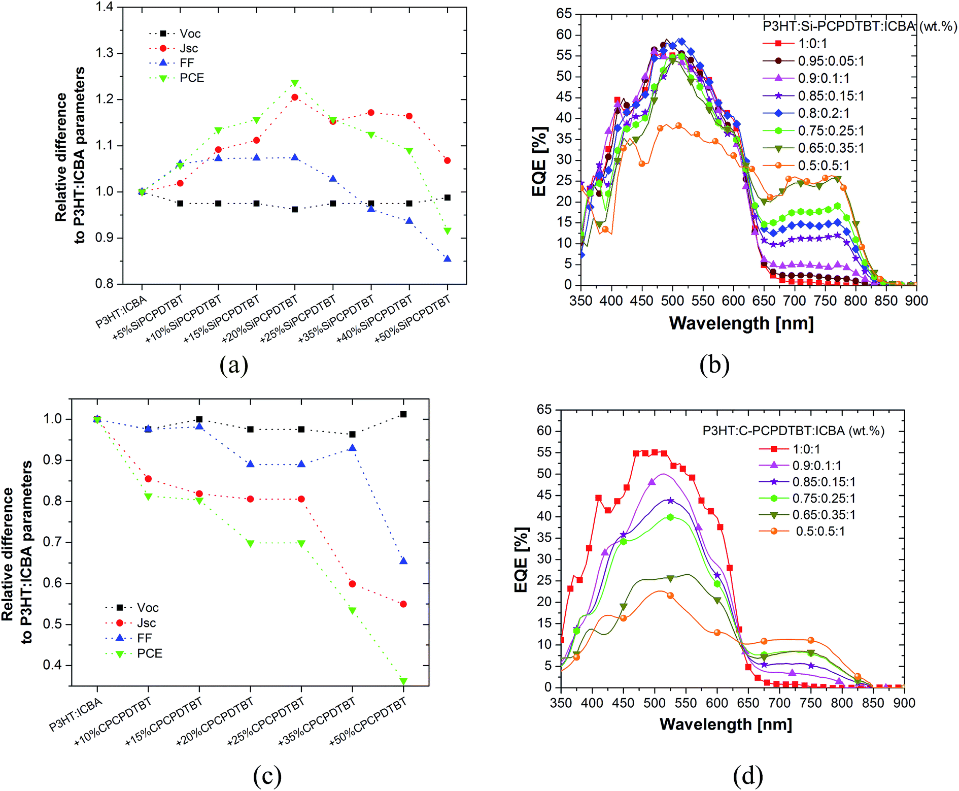 | ||
| Fig. 2 (a) Relative changes of device parameters with increasing (a) Si-PCPDTBT and (c) C-PCPDTBT content. The performance of binary P3HT:ICBA is chosen as the reference and set to 100%. All other device data are normalized to that reference; (b) EQE spectra of (b) P3HT:Si-PCPDTBT:ICBA and (d) P3HT:C-PCPDTBT:ICBA devices with different sensitizer contents under AM1.5G, 100 mW cm−2 illumination. | ||
When increasing the Si-PCPDTBT content up to 20 wt% the short circuit current density (Jsc) increases remarkably from 7.95 to 10 mA cm−2. At Si-PCPDTBT contents larger than 20 wt%, JSC drops slightly but remains higher than the value obtained for the binary P3HT:ICBA device. The open circuit voltage (Voc) is nearly unaffected by the addition of Si-PCPDTBT. Here, the slight drop of 3% in Voc is likely due to the change in the recombination mechanism.18 As for the ternary P3HT:Si-PCPDTBT:PCBM system, the fill factor improves around 8% at the optimized composition ratio of 80:20:100 wt% (FF ∼ 65%), compared to the corresponding binary P3HT:ICBA system (FF ∼ 60%). Finally, at concentrations beyond 50 wt% a substantial reduction is observed (FF < 55%). As Fig. S3† documents, the maximum values were reproduced for 18 samples at each concentration. Here, the key parameters are plotted with error bars.
The EQE spectra for P3HT:ICBA and for ternary cells with 5–50 wt% Si-PCPDTBT are presented in Fig. 2b. As such, they corroborate the NIR sensitization by Si-PCPDTBT in the 650–850 nm range, where the P3HT:ICBA contribution to EQE is negligible. In the long wavelength region the external quantum efficiency increases by increasing the Si-PCPDTBT sensitizer content and saturates at a sensitizer concentration of 50 wt% at 25% EQE. Samples with Si-PCPDTBT contents up to 20 wt% exhibit similar EQE in the P3HT absorption range, namely 400 to 600 nm, as the binary P3HT:ICBA reference. Slight variations might be due to differences in the active layer thicknesses or the optical interference within 100 nm thin active layers in the 400–600 nm region. At Si-PCPDTBT concentrations higher than 20 wt%, the EQE in the P3HT absorption range decreases due to a lower amount of P3HT, while at concentrations of 50 wt% a substantial drop in EQE is observed. In conclusion, the most efficient device, comprising 20 wt% Si-PCPDTBT, shows nearly an EQE plateau of 15% in the range of 650–800 nm and a maximum peak of ∼ 60% in the P3HT absorption range.
In contrast to Si-PCPDTBT, addition of C-PCPDTBT as an NIR sensitizer to the P3HT:ICBA blend did not result in any performance improvement, and appeared to adversely impact both Jsc and FF – see Fig. 2c and S4.† The reduction in Jsc happens in two recognizable steps. First, when the content of the sensitizer is at 10 to 25 wt%, Jsc drops around 20% compared to the reference binary system. In the second step and at higher sensitizer concentrations, Jsc shows a further decrease of 50 to 60%. The corresponding EQE spectra of these solar cells represent a minor contribution of the sensitizer in the long wavelength region of 650–850 nm (Fig. 2d); this increase is however accompanied by a continuous and considerable decrease of the EQE within the 400–600 nm region, where the host system of P3HT:ICBA has a dominant contribution. For instance, adding 10 wt% C-PCPDTBT increases the EQE around 3% in the near IR region, while an EQE reduction of 5–10% is observed all over the 400–600 nm region. We cannot assign this great loss only to the 10 wt% lower concentration of P3HT. The slight EQE increase in the near IR region cannot compensate for the significant EQE loss in 400–600 nm regions, leading, in turn, to an overall Jsc loss. Concurrent with the Jsc loss, we observe a decrease in the FF. This drop is rather moderate at low sensitizer concentrations, and becomes more pronounced for concentrations higher than 20 wt%. The Voc loss of 3% is also observed compared to the reference P3HT:ICBA device. Overall, we can conclude that the addition of even a low concentration of the C-PCPDTBT can be detrimental to the power conversion efficiency of the P3HT:ICBA device. The corresponding J–V characteristics are presented in Fig. S2b† and the performance key parameters are tabulated in Table 1.
2.2 Morphology investigation
Employing various techniques, we carried out a comprehensive study on the morphology of ternary P3HT:Si-PCPDTBT:ICBA, P3HT:C-PCPDTBT:ICBA and P3HT:Si-PCPDTBT:PCBM systems. We have reported the studies of the morphology of ternary P3HT:C-PCPDTBT:PCBM elsewhere.8,17UV-Vis spectroscopy. Absorption spectra of the binary and ternary films with a thickness of around 100 nm are presented in Fig. 3a. Addition of 20 wt% Si-PCPDTBT to P3HT:ICBA results in an absorption peak in the range between 650 and 850 nm, where P3HT fails to contribute to the overall absorbance. With increasing sensitizer content, the contribution of P3HT decreases, whereas the Si-PCPDTBT absorption increases. However, with respect to optimized device performance (80
:20:100 wt% P3HT:Si-PCPDTBT:ICBA), the P3HT absorption is not significantly reduced, when compared to the P3HT:ICBA reference. The absorption peaks of P3HT and their typical aggregation related shoulders at 550 and 600 nm are also visible when high Si-PCPDTBT concentrations are present. From the latter we conclude that the π–π stacking of P3HT is not crucially perturbed by addition of up to 40 wt% Si-PCPDTBT.
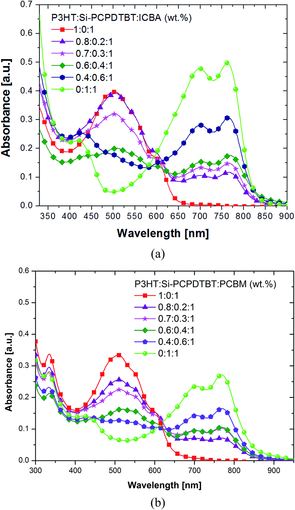 | ||
| Fig. 3 Absorbance spectra of P3HT:Si-PCPDTBT:ICBA (a) and P3HT:Si-PCPDTBT:PCBM (b) films with different Si-PCPDTBT sensitizer contents. | ||
The UV-Vis spectra of P3HT:C-PCPDTBT:ICBA with the sensitizer content less than 40 wt% show behavior very similar to that of the ternary composite comprising Si-PCPDTBT (Fig. S5†). The comparable absorption contribution of the C-bridged sensitizer in the 650–850 nm region and the similarly unaffected π–π stacking shoulder of P3HT indicate that Jsc loss can be attributed to neither low absorption of the sensitizer, nor the noticeable disturbed P3HT ordering.
Atomic force microscopy (AFM). Fig. 4a–h show non-contact mode AFM images. For P3HT:ICBA, a smooth surface with a root-mean-square roughness of Rrms = 1.3 nm (Fig. 4a) is noted. In analogy to the ternary P3HT:Si-PCPDTBT:PCBM systems,13 no change of the surface topography is observed by adding up to 40 wt% Si-PCPDTBT. The surface roughness and domain sizes (Fig. 4b and c) are comparable to those seen for P3HT:ICBA. This observation suggests that there is little interaction between Si-PCPDTBT and either P3HT or ICBA. Ternary composites with 60 and 70 wt% Si-PCPDTBT exhibit larger domain sizes and higher surface roughness with values of 11 and 10 nm, respectively, suggesting considerable morphological changes (Fig. 4d and e). In ternary films containing 80 wt% Si-PCPDTBT (Rrms = 6.5 nm) and 90 wt% Si-PCPDTBT (Rrms = 4.7 nm) (Fig. 4f and g) smaller domain sizes converge towards the characteristics of the binary Si-PCPDTBT:ICBA film (Rrms = 3.7 nm). Please also note that the binary Si-PCPDTBT:ICBA film (Fig. 4h) shows features different from those of the P3HT:ICBA reference.
 | ||
| Fig. 4 Non-contact mode AFM surface scans of 1:1 wt% P3HT:ICBA (a); 0.8:0.2:1 (b), 0.6:0.4:1 (c), 0.4:0.6:1 (d), 0.3:0.7:1 (e), 0.2:0.8:1 (f), and 0.1:0.9:1 wt% P3HT:Si-PCPDTBT:ICBA (g); and 1:1 wt% Si-PCPDTBT:ICBA (h). | ||
Interestingly, AFM images of the ternary P3HT:C-PCPDTBT:ICBA systems show a very different trend (Fig. S6†). At 20 wt% C-PCPDTBT concentration, no specific changes are observed in surface topography. In this case, only a minor change in the surface roughness is found (Rrms = 0.8 nm). At sensitizer contents up to 70 wt%, the films show slightly finer features with a Rrms of around 0.6 nm. For sensitizer contents above 70 wt%, ternary films show surface features very similar to those of the binary C-PCPDTBT:ICBA film with a Rrms of <0.5 nm. These results suggest that C-PCPDTBT forms a very fine intermixing with the host system, either in one of the P3HT and ICBA phases or both. Noticeably, the C-PCPDTBT:ICBA shows much finer features at the surface compared to Si-PCPDTBT:ICBA or P3HT:ICBA systems.
Surface energy. Surface energy has been shown to play a decisive role in the segregation of components. Previous studies have indicated that the location of a component in a ternary system can be predicted from the knowledge of the surface energies of all components.23–27 We also consider the surface energy of the materials as an important factor determining the sensitizer localization in the ternary blend films. Contact angle measurements were used to determine the surface energies of the pristine components as well as the binary and ternary composites with different mixing ratios. The surface energy of C-PCPDTBT (γC-PCPDTBT = 40.5 ± 1.5 mN m−1) is much higher than that of Si-PCPDTBT (γSi-PCPDTBT = 26.4 ± 2.1 mN m−1). Pristine P3HT and PCBM showed surface energies of 27.4 ± 0.8 and 45.8 ± 1.8 mN m−1, respectively. The surface energy of pristine ICBA (γICBA = 46 ± 1.4 mN m−1) is nearly equal to that of PCBM. The wetting coefficient of a guest material C (ωC) in blends of host materials A and B, which determines the location of the low bandgap polymeric sensitizers in ternary blends, is calculated on the basis of the interfacial surface energies between the pristine materials. If the wetting coefficient is larger than unity (ωC > 1), C will be located in domains of A. If ωC < −1, C will be located in domains of B. If −1 < ωC < 1, C will be located at the interface between domains of A and B. To simplify the calculations, following assessments are based on the averages of γP3HT = 27.4 and γICBA = γPCBM = 46 mN m−1, without considering their standard deviations. As such, the wetting coefficient of C-PCPDTBT in P3HT:ICBA and P3HT:PCBM was calculated to be −0.4 ± 0.2. Therefore, C-PCPDTBT is most likely located at the P3HT:ICBA and P3HT:PCBM interfaces with the tendency to interact with the semi-crystalline (or aggregated) domains of either ICBA or PCBM. In contrast, the calculated wetting coefficient of 1.1 ± 0.2 for Si-PCPDTBT in the P3HT:ICBA and P3HT:PCBM blends suggests that Si-PCPDTBT is located in the amorphous P3HT domains at the P3HT:ICBA or P3HT:PCBM interfaces with a high tendency to interact with the crystalline domains of P3HT.
We also determined the surface energies of P3HT:Si-PCPDTBT, Si-PCPDTBT:ICBA and Si-PCPDTBT:PCBM as well as P3HT:Si-PCPDTBT:ICBA and P3HT:Si-PCPDTBT:PCBM films. The surface energies of the ternary blends, adding different concentrations of Si-PCPDTBT to P3HT:ICBA and P3HT:PCBM, follow a similar trend as observed for the P3HT:Si-PCPDTBT binary systems (Fig. S7, S8 and Tables S1, S2†). These findings suggest that an interaction between P3HT and Si-PCPDTBT polymers is more probable than an interaction between either ICBA or PCBM and Si-PCPDTBT.
Photoluminescence (PL). The PL spectra (excitation at 488 nm) of the pristine components (P3HT, sensitizer, and ICBA), the binary composites (P3HT:ICBA and sensitizer:ICBA), and the ternary composites featuring varying Si-/C-PCPDTBT sensitizer concentrations are depicted in Fig. S9† and 5. The spectra have been normalized to the absorbance of each film at 488 nm. The absorption coefficients (α) of P3HT and Si-PCPDTBT films at 488 nm are 8.7 × 10428 and 2.6 × 104 cm−1,29 respectively. The penetration depths of the excitation light, 1/α, into P3HT and Si-PCPDTBT films are around 115 and 385 nm, respectively. In light of this consideration, the PL represents the bulk and not only the film surfaces. The PL of P3HT and Si-PCPDTBT films peaks at 740 and 860 nm, respectively (Fig. S9a†). In the binary polymer:ICBA 1
:1 wt% blends, the PL of P3HT and Si-PCPDTBT is quenched by around 80 and 95% (Fig. 5a with an enlarged PL intensity scale). Adding 20 wt% Si-PCPDTBT to P3HT:ICBA reduces the PL by about 25% at the P3HT PL peak at 740 nm. This decrease is accompanied by a small enhancement of the Si-PCPDTBT PL at 860 nm. Increasing the Si-PCPDTBT content beyond 20 wt% leads to a further decrease of the P3HT PL intensity (∼90%), whereas the Si-PCPDTBT PL intensity gradually increases. In accordance with the surface tension measurements, this might be explained by the growth of Si-PCPDTBT domains inside or at the phase boundaries of P3HT domains. Such sensitizer phases would decrease the effective size of P3HT domains, resulting in reduced P3HT PL intensities. The increasing Si-PCPDTBT PL might originate from increasing size of sensitizer domains, which maximize at around 70 wt% Si-PCPDTBT according to the AFM results. Previously, we implied a hole transfer from Si-PCPDTBT to P3HT upon electron transfer from Si-PCPDTBT to fullerene.15 Interestingly, at Si-PCPDTBT contents above 70 wt%, the Si-PCPDTBT PL starts to decrease towards the PL of the Si-PCPDTBT in the binary blend with ICBA, which indicates decreasing domain sizes (Fig. 5a). This observation is consistent with the AFM analysis, which reveals that above 70 wt% Si-PCPDTBT the domains reduce in size and converge to sizes observed for Si-PCPDTBT:ICBA. In line with the device performance and AFM images, the PL spectra of P3HT:C-PCPDTBT:ICBA ternary systems show a different trend compared to those of Si-PCPDTBT ternary systems. By adding 20 wt% C-PCPDTBT the PL intensity of P3HT:ICBA is quenched by over 50%, and simultaneously the C-PCPDTBT shows a considerable PL increase in the 800–1100 nm region (Fig. 5b), despite the absence of larger domains of C-PCPDTBT in the blend based on our AFM images. We may partly relate this to the higher PL of C-PCPDTBT compared to Si-PCPDTBT. Interestingly, the pristine C-PCPDTBT and its blend with ICBA both show a higher PL compared to pristine Si-PCPDTBT and Si-PCPDTBT:ICBA blend (Fig. S9b vs. S9a† and Fig. 5avs.5b). As mentioned previously, the PL intensities are normalized to the film absorption cross-sections at the excitation wavelength; therefore we rule out the possible influence of light absorption variation on the difference observed in PL intensity. Upon increasing the C-PCPDTBT content beyond 20 wt%, films show only a negligible PL emission for P3HT:ICBA, whereas the PL intensity of C-PCPDTBT shows further increase and remains unchanged for C-PCPDTBT contents up to 70 wt%. For the systems containing above 70 wt% sensitizer, PL slightly lower but comparable with that of the C-PCPDTBT:ICBA system is observed. On the basis of surface tension measurements, AFM analysis and PL spectra, we infer that, on one hand, the situated C-PCPDTBT at the P3HT and ICBA interfaces efficiently quenches the P3HT:ICBA PL emission and on the other hand, another part of the sensitizer interacts mainly with semi-crystalline/aggregated fullerene zones and forms a very fine intermixing with ICBA even at low C-PCPDTBT concentrations. Such fine morphology can disturb the efficient electron transport within the ternary blends, and also negatively impact the efficient extraction of the free holes from the sensitizer. The strongly reduced EQE in the 400–600 nm region (P3HT:ICBA contribution) and small increase of EQE in the near IR region (C-PCPDTBT contribution) confirm this hypothesis.
 | ||
| Fig. 5 Photoluminescence (PL) spectra of P3HT:sensitizer:ICBA films containing different amounts of (a) Si-PCPDTBT and (b) C-PCPDTBT sensitizers; the inset presents the PL intensity at 860 nm versus different sensitizer concentrations. | ||
Space charge limited current (SCLC). In order to obtain additional insights into the transport properties of P3HT:Si-/C-PCPDTBT:ICBA blends, we carried out space charge limited current (SCLC) measurements to individually characterize the hole and electron mobility of different blends. Fig. 6a shows the measured electron and hole mobility in P3HT:ICBA as a function of sensitizer content. The balanced hole and electron mobility values of P3HT:ICBA (μe,P3HT:ICBA = 1.9 × 10⁻⁴ cm2 V−1 s−1 and μh,P3HT:ICBA = 1.6 × 10⁻⁴ cm2 V−1 s−1) are in agreement with reported results from Kang et al.30 Addition of 10 wt% Si-PCPDTBT into the P3HT:ICBA host system leads to a deterioration of the electron and hole mobility to a different extent (μe,P3HT:Si-PCPDTBT:ICBA = 8.14 × 10⁻⁵ cm2 V−1 s−1 and μh,P3HT:Si-PCPDTBT:ICBA = 3.8 × 10⁻⁵ cm2 V−1 s−1). Compared to the binary reference system, the reduction in hole mobility is around 55% larger than the decrease in electron mobility. For the sensitizer contents above 10 wt%, the decrease in hole mobility vs. electron mobility is even more pronounced. At high Si-PCPDTBT contents (above 50 wt%), the hole mobility surpasses slightly the electron mobility. For sensitizer concentrations (20–30 wt%), at which the devices perform efficiently, the electron mobility reaches a plateau of around 5 × 10⁻⁵ cm2 V−1 s−1 and the measured hole mobility is still in the acceptable range of around 1 × 10⁻⁵ cm2 V−1 s−1. Further reduction in mobility appeared to be detrimental to the device functionality. In contrast to the Si-PCPDTBT, the addition of C-PCPDTBT to the host matrix influences noticeably the electron mobility rather than the hole mobility. Based on presented results and specifically our surface tension analysis, this different behavior can be explained by a higher interaction of C-PCPDTBT with fullerene semi-crystallites which reduces the order of the fullerene phase and thus the electron mobility. Conversely, Si-PCPDTBT impacts mainly the P3HT crystallites and deteriorates the ordering of the P3HT matrix leading to a major reduction in the hole mobility. These findings suggest that, here, the perturbation of the electron transport is more deleterious to the device performance. Moreover, the drop in Jsc and FF even at low C-PCPDTBT concentrations suggests that P3HT:C-PCPDTBT:ICBA ternary systems suffer from more critical transport issues and higher recombination losses when compared to the ternary system of P3HT:C-PCPDTBT:PCBM. As mentioned previously, the latter can be related to the less ordering of P3HT:ICBA compared to the P3HT:PCBM.
 | ||
| Fig. 6 SCLC electron and hole mobility vs. sensitizer (Si-PCPDTBT and C-PCPDTBT) content added to the (a) P3HT:ICBA and (b) P3HT:PCBM host systems. The electron and hole mobility values of the P3HT:C-PCPDTBT:PCBM systems are extracted from ref. 15. | ||
UV-Vis spectroscopy. Absorption spectra of the binary and ternary blends are presented in Fig. 3b. When increasing the sensitizer content a continuous reduction in the P3HT absorption (400–650 nm) and an increase in Si-PCPDTBT absorption (650–850 nm) are noted. In agreement with P3HT:Si-PCPDTBT:ICBA, π–π stacking of P3HT is unaffected up to 40 wt% Si-PCPDTBT.
Grazing incidence wide-angle X-ray scattering (GIWAXS). The GIWAXS measurements were performed on films prepared from pristine components (P3HT, Si-PCPDTBT, and PCBM), the binary composites (P3HT:PCBM and Si-PCPDTBT:PCBM), and ternary composites of P3HT:Si-PCPDTBT:PCBM containing 20, 40 and 60 wt% sensitizer. Fig. 7 summarizes the two-dimensional detector pattern, shown in (q, Φ)-presentation. Here, q is the overall momentum transfer and Φ denotes the angle between the directions parallel (Φ = 0°) and perpendicular (Φ = 90°) to the sample surface. For more details on the experimental setup and data conversion see ref. 31. To compare the polymer scattering contributions in samples containing different amounts of polymer, data in Fig. 7 are normalized to the polymer content and are plotted on the same intensity scale. For a comparison of the PCBM features, Fig. S11† shows the same data normalized to the PCBM content. Further details on the compound's content normalization are presented in section 8.3 of the ESI.†
 | ||
| Fig. 7 Two-dimensional GIWAXS detector patterns in (Φ [°], q [nm−1])-presentation of pristine, binary and ternary P3HT:Si-PCPDTBT:PCBM films with (x:1 − x:y) weight ratio. (1) Pristine polymer films (y = 0): P3HT (Ia: x = 1) and Si-PCPDTBT (Ie: x = 0). (2) Binary films: P3HT:PCBM (IIa: y = 1, x = 1, and IIIa: y = 4, x = 1) and Si-PCPDTBT:PCBM (IIe: y = 1, x = 0, and IIIe: y = 4, x = 0). (3) Ternary films (y = 1): 0.8 (IIb), 0.6 (IIc), 0.4 (IId) and corresponding artificial polymer blend spectra (Ib, Ic, and Id) calculated under the assumption that the P3HT (Ia) and Si-PCPDTBT (Ie) spectra simply superimpose. Intensity scales are adjusted to the polymer volume fraction. Corresponding spectra normalized to the PCBM volume fraction are presented in the ESI (Fig. S11†). | ||
The degree of order in P3HT films is high (Fig. 7Ia). The interlayer peak (q = 3.96 nm−1, d = 1.59 nm, Φ = 90°), which originates from the layered structures of the conjugated backbones separated by layers of the alkyl side chains, is narrow and high in intensity. Higher order peaks are also visible. The peak at q = 16.8 nm−1 (d = 0.374 nm, Φ = 0°) relates to π–π stacking perpendicular to the interlayer stacking. Notably, the results are comparable to those of our previous work.17 Domains orient preferably in an edge-on configuration (interlayer peak at Φ = 90°) with some isotropic orientations that stem most likely from the bulk of the film.
Compared to P3HT, the Si-PCPDTBT is less organized (Fig. 7Ie and S10d†). However, the degree of order is significantly higher than that seen for C-PCPDTBT.17 The peak at q = 3.70 nm−1 (d = 1.70 nm, Φ = 90°) correlates with domains with preferred edge-on orientation relative to the substrate. However, besides the isotropic orientation some preferences for face-on orientation (q = 17.76 nm−1, d = 0.354 nm, Φ = 90°) are also observed.
In accordance with previous reports,17 the PCBM film shows three broad peaks (q = 7.3, 13.8 and 20.6 nm−1) (Fig. S11I†). PCBM domains do not exhibit long range order and there is no preferred domain orientation relative to the substrate (isotropic scattering).
For the following discussion, we will take the peak intensity of the main PCBM peak at about 14 nm−1 as a measure of the degree of phase separation (at same PCBM content) or, more generally spoken, as a measure of the amount of pristine PCBM phase. Please, note that the main PCBM peak corresponds to nearest neighbor correlations. Thus GIWAXS rather measures the amount of neat PCBM phase but not necessarily its crystallinity. This can lead to differences in the results derived from GIWAXS and DSC.17 For comparison of the PCBM and polymer peak intensities, the spectra obtained for the films prepared from binary and ternary mixtures are scaled according to the PCBM and polymer volume fraction in the blend. For more details see the ESI,† section 8.3.
For the binary films, Fig. 8a presents the polymer interlayer peak heights normalized to those of the respective pristine polymer films as a function of the PCBM content. In accordance with previous results,17 in the P3HT:PCBM 1:1 wt% film the degree of polymer order is preserved compared to that for pristine P3HT (Fig. 7IIa). It seems that in comparison to the pristine P3HT film the preference for edge-on orientation is somewhat more limited to the surface regions of the film, as indicated by the smaller angular spread of the interlayer peak – please compare Fig. 7IIa and Ia. In addition, we noted a slight preference for face-on orientations in the domains (see e.g. π–π stacking peak at Φ = 90° and 0°). A reduced crystallinity in the bulk of the film with isotropic domain orientations as reported previously is, however, not observed.17
 | ||
| Fig. 8 GIWAXS intensity of the main polymer interlayer peak (a and c) and main PCBM peak (b and d) normalized to the peak intensity of the corresponding pristine polymer and PCBM film, respectively, as a function of the Si-PCPDTBT (c and d) and PCBM contents (a and b). | ||
In the Si-PCPDTBT:PCBM 1:1 wt% film, the degree of polymer order is also preserved in the presence of the PCBM – please compare Fig. 7IIe and Ie. In fact, the increase in polymer interlayer peak height indicates an enhanced preference for edge-on orientations in the Si-PCPDTBT:PCBM films when compared to the pristine Si-PCPDTBT films (Fig. 8a). The isotropic contribution to the scattering decreases only slightly. An increase of the PCBM weight fraction to 80% leads to a strong reduction in the polymer crystallinity. This effect is more pronounced for P3HT than for Si-PCPDTBT (Fig. 7IIIa and IIIe). The Si-PCPDTBT shows enhanced order close to the surface and/or film-substrate interface. The polymer interlayer peak further increases in height (Fig. 8a), but some residual order remains in the bulk of the films. For both systems, PCBM is most likely incorporated into the amorphous part of the polymer. At lower PCBM contents (1:1 wt%) the presence of PCBM does not lead to any significant impact on the polymer crystallization. In the 1:1 wt% films the poorly organized Si-PCPDTBT obviously shows a higher polymer-PCBM-intermixing tendency than the more crystalline P3HT. For the binary films, Fig. 8b presents the PCBM peak heights normalized to that of the pristine PCBM film as a function of PCBM – see also two-dimensional data in Fig. S11.† The peak height of the main PCBM peak of the P3HT:PCBM 1:1 wt% film is comparable to that of pristine PCBM films, whereas the intensity of that of the Si-PCPDTBT:PCBM film is clearly reduced, which is in sound agreement with a recent report for P3HT and C-PCPDTBT.17 Increasing the PCBM content to 80 wt% leads to a further reduction of the PCBM peak intensities. However, this trend is less pronounced for Si-PCPDTBT than for P3HT, which is in accordance with the observation that further PCBM addition has less impact on the Si-PCPDTBT crystallinity than on that of P3HT.
Finally, we compared the experimental spectra obtained for ternary P3HT:Si-PCPDTBT:PCBM films (Fig. 7IIb–d) to that expected by just superimposing the spectra of the pristine polymer films according to their volume fraction (Fig. 7Ib–d) (see also section 8.3 in the ESI†). Fig. 8c shows the polymer interlayer peak intensity measured and computed for the ternary films as a function of the sensitizer content. Overall, they are indistinguishable. In the ternary films the crystallinity of the polymer phase is, however, somewhat reduced compared to that seen in the pristine polymer films. At a sensitizer content of 20 wt%, the polymer phase is still crystalline. At higher Si-PCPDTBT contents the higher order scattering features of the P3HT interlayer peak and the π–π peak at Φ = 0° start disappearing (40 wt%) or are lacking (60 wt%). In contrast, the Si-PCPDTBT π–π peak of the face-on domains at Φ = 90° remains (the corresponding π–π peak of P3HT would appear at smaller q-values). The interlayer peak intensity is close to the value obtained for the binary Si-PCPDTBT. It seems that the presence of Si-PCPDTBT is detrimental to the ordering process of P3HT, whereas the Si-PCPDTBT ordering in the ternary films remains or is marginally affected.
In the P3HT:Si-PCPDTBT:PCBM 0.8:0.2:1 wt% film the degree of P3HT crystallinity and the degree of PCBM phase separation are high (Fig. 7IIb and S11IIb†). Fig. 8d shows the PCBM peak intensity obtained for the ternary films as a function of the sensitizer content. The PCBM signal is only slightly reduced compared to that of the P3HT:PCBM 1:1 wt% film. The addition of 20 wt% Si-PCPDTBT has no significant effect on the PCBM phase and also the P3HT crystallinity is to a large extent preserved. Increasing the Si-PCPDTBT fraction beyond 20 wt% leads to a reduction of the amount of PCBM phase (Fig. S11IIc and d†). However, the relative reduction of the PCBM peak intensity is notably lower compared to that observed for the polymer interlayer peak – please compare Fig. 7c and d. This suggests that the intensity reduction stems not only from PCBM incorporation but also from incorporation of Si-PCPDTBT domains into the P3HT phase.
In conclusion, the GIWAXS results confirm that Si-PCPDTBT exerts less impact on the semi-crystalline domains of PCBM than C-PCPDTBT.17 The addition of the sensitizer seems to be detrimental to the P3HT ordering, whereas Si-PCPDTBT is marginally affected. Si-PCPDTBT as well as PCBM are most likely incorporated into the P3HT phase at high sensitizer concentrations. These results are consistent with our prediction based on interfacial surface energy calculations.
Space charge limited current (SCLC). Fig. 6b shows the measured electron and hole mobility in P3HT:PCBM as a function of Si-PCPDTBT content. For a direct comparison, the electron and hole mobility in P3HT:PCBM as a function of the C-PCPDTBT sensitizer content is taken from ref. 17 and is also presented in the same graph. The electron mobility is rather constant up to 60 wt% Si-PCPDTBT after a slight drop from 2.3 × 10⁻³ to 1 × 10⁻³ cm2 V−1 s−1 upon addition of 20 wt% sensitizer to P3HT:PCBM. In contrast, at sensitizer contents above 40 wt% the hole mobility changes from 2.7 × 10⁻⁴ down to 4.8 × 10⁻⁵ cm2 V−1 s−1. At these concentrations, the fill factor is lowered (Fig. S1d†). For P3HT32 and Si-PCPDTBT-based systems,33 space-charge formation becomes significant when the difference between the electron and hole mobility values is larger than 2–3 orders of magnitude. The diminished hole mobility does not influence the space-charge formation of the photocurrent. The binary blend of Si-PCPDTBT:PCBM shows an electron mobility of μe,Si-PCPDTBT:PCBM = 2.8 × 10⁻⁴ and a hole mobility of μh,Si-PCPDTBT:PCBM = 6.5 × 10⁻⁴ cm2 V−1 s−1. Conversely, for the P3HT:C-PCPDTBT:PCBM ternary systems a substantial reduction in electron mobility is observed, while the hole mobility stays unchanged.
In agreement with the surface tension prediction and GIWAXS results, the SCLC results confirm that Si-PCPDTBT exhibits tighter interaction with the amorphous P3HT:ICBA and P3HT:PCBM interfaces and semicrystalline domains of P3HT than the semicrystalline, aggregated domains of either ICBA or PCBM. This allows us to fabricate high efficiency ternary P3HT:Si-PCPDTBT:ICBA and P3HT:Si-PCPDTBT:PCBM devices with over 60% FF at sensitizer concentrations of 20 to 40 wt%. In contrast, the C-PCPDTBT sensitizer has a detrimental effect on the semicrystalline domains of the fullerene derivatives, impairing the device performance drastically even at very low concentration for P3HT:ICBA and at concentrations over 20 wt% for P3HT:PCBM reference systems.17,34
3. Conclusion
The performance of ternary solar cells based on P3HT:PCBM and P3HT:ICBA host matrices was improved by over 25% using 20–40 wt% of the near-IR sensitizer Si-PCPDTBT, while no drop in fill factor was observed. In contrast, no considerable device improvement was found when using C-PCPDTBT as the sensitizer for host systems of P3HT:PCBM and P3HT:ICBA. In the latter case, the addition of even a small amount of C-PCPDTBT to P3HT:ICBA deteriorated the device performance due to a substantial decrease in Jsc and FF. These performance losses are correlated with a substantial decreased electron mobility that is caused by preferential mixing of C-PCPDTBT with ICBA. The interfacial surface energy results indicated that Si-PCPDTBT locates at amorphous interfaces and P3HT crystallites, while C-PCPDTBT tends to accumulate at amorphous interfaces and semi-crystalline (or agglomerated) domains of the fullerene derivatives. GIWAXS and SCLC results are in agreement with this scenario. This study shows how slight structural modifications can significantly impact the behavior of a complex multiphase system. As an initial set of design rules we showed that the surface energy of the sensitizer is an important parameter to control the morphology of ternary blends. By designing sensitizers bearing fine-tuned surface energy, using appropriate functional groups, it is possible to incorporate these materials into the donor or into the acceptor phase. For instance in systems with low electron mobility (like the P3HT:ICBA), it is beneficial to use a sensitizer that prefers to mix with the polymer, as this will have less negative effects on the electron mobility. For these systems the disruption of the fullerene semi-crystalline domains is more detrimental to the device performance than the disruption of the polymer domains. The degree of crystallinity of the sensitizer might also impact the device performance. However, for the specific ternary systems investigated in this study this theory is not supported by our SCLC results.The current study can be used as a guideline for the establishment of design rules for organic ternary solar cells. However, further systems with different electronic energy levels, transport properties and crystallinity need to be examined. A comprehensive understanding of the morphology, charge transfer and charge transport in ternary systems can pave the way to high performance organic ternary solar cells.
4. Experimental section
4.1 Device fabrication
All the devices were fabricated in an inverted architecture (see Fig. 1b). Pre-structured indium tin oxide (ITO) coated glass substrates (Nuremberg Weidner Glas GmbH) were cleaned in acetone and isopropyl alcohol. After drying, the substrates were coated with Al-doped zinc oxide (AZO).35 The photoactive solutions were prepared from P3HT (purchased from Merck with 96.6% regioregularity) and Si-PCPDTBT (provided by Konarka) with different mixing ratios but constant overall polymer concentration of 1 wt% in o-dichlorobenzene/or chlorobenzene blended with ICBA (purchased from 1-Material) and PCBM (purchased from Solenne BV), respectively, with the polymer:fullerene ratio of 1:1. The active layers with an approximate thickness of 100 nm were doctor bladed from the as-prepared solutions on top of the AZO layer. Afterward the electron blocking layer of poly(3,4-ethylene dioxythiophene) doped with (polystyrene sulfonic acid) (PEDOT:PSS, purchased from Heraeus) diluted in isopropyl was bladed. The whole stack was annealed on a hot plate at 150 °C for 10 min. To complete the device preparation, a 100 nm thick Ag layer was evaporated as the top electrode. The active area was 10.4 mm2. All solution-processed layers were bladed in ambient air.
4.2 J–V and EQE characterization
The J–V characteristics were measured under AM1.5G illumination at 100 mW cm−2 (OrielSol 1A Solar simulator) using a source measurement unit from BoTest. The EQE spectra were recorded with a Varian CARY 500 Scan spectrometer with a tungsten light source.4.3 Surface and absorption characterization
AFM measurements were performed with a Veeco Model 03100 in non-contact mode after 10 min thermal annealing at 150 °C. For the film absorbance and thickness measurements UV-Vis-NIR spectrometer (Lambda 950, from Perkin) and Tencor profilometer were employed, respectively. The contact angle between the three solvents' drops (ultrapure water, diiodomethane and ethylene glycol) and the surface of the bladed and annealed films of pristine materials and their binary and ternary blends were measured using a contact angle instrument from Dataphysics (model OCA20). With the values of the initial contact angles, surface energies were calculated using the SCA20-U software and the Owens–Wendt and Kaelble method.36 The given surface energies for the pristine materials are averaged values based on 10 measurements per film. The wetting coefficient of material C (ωC) in blends of materials A and B can be calculated by Young's equation ωC = (γC–B − γC–A)/γA–B, where γX–Y is the interfacial surface energy between X and Y,23 calculated by Neumann's equation γX–Y = γX + γY – 2(γXγY)0.5exp[−β(γX − γY)2], where β = 0.000115 m4 mJ−2.37
4.4 Photoluminescence (PL)
For the PL measurement, the films were excited at 488 nm by a chopped argon laser beam. The PL emission of the films was dispersed by a 600 lines per mm grating monochromator (HRS-2) and detected by a Germanium detector (ADC 403L) through the lock-in technique.4.5 Space charge limited current (SCLC)
The structures of the hole only and electron only devices were glass/ITO/PEDOT:PSS/active layer/PEDOT:PSS/Ag and glass/ITO/AZO/active layer/Ca/Ag, respectively. The J–V characteristics of the single charge carrier devices were measured under dark conditions and analyzed in the space charge limited region. The charge carrier mobility is determined by a fit of the modified Mott–Gurney equation: to the measured J–V curves, where JSCL is SCL current density, ε0 and εr are the electric permittivity of free space and the relative dielectric constant of the active layer respectively, μ is the charge carrier mobility, L is the thickness of the device and β is the electric field-activation factor of mobility and accounts for the degree of disorder. Vin is the voltage drop across the sample, Vin = V − Vbi − Vrs, where V is the applied voltage, Vbi the built-in voltage and Vrs is the voltage drop due to the series resistance of the contacts.38
4.6 Grazing incidence wide-angle X-ray scattering
We performed grazing incidence wide-angle X-ray scattering experiments at the BW4 beam line, at HASYLAB at DESY in Hamburg, Germany. Experiments were carried out in the pseudo-grazing incidence configuration at a wavelength of λ = 0.138 nm, a band width of 10−4 and a spot size of 78 μm × 46 μm in horizontal and vertical directions, respectively. The incident polar angle was set to αi = 0.20°. Two-dimensional detector patterns were collected with an exposure time of 900 s on a CCD-detector (MAR165CCD, pixel size: 79.1 μm). The detector to sample distance was determined by means of a silver behenate standard. Data are corrected for background scattering from the silicon substrate and are normalized to the film thicknesses and incoming flux in order to allow for a comparison of peak intensities between different samples.Acknowledgements
The authors gratefully acknowledge the support of the Cluster of Excellence “Engineering of Advanced Materials” at the University of Erlangen-Nuremberg, which is funded by the German Research Foundation (DFG) within the framework of its “Excellence Initiative”, Organic Semiconductors for NIR Optoelectronics (OSNIRO, grant no. 607585) and Synthetic Carbon Allotropes (SFB953). This work has been funded by the DFG project, grant no. BR 4031/2-2 and Solar Technologies go Hybrid (SolTech).References
- M. A. Green, K. Emery, Y. Hishikawa, W. Warta and E. D. Dunlop, Prog. Photovoltaics, 2012, 20, 12 Search PubMed.
- J. You, L. Dou, K. Yoshimura, T. Kato, K. Ohya, T. Moriarty, K. Emery, C. C. Chen, J. Gao, G. Li and Y. Yang, Nat. Commun., 2013, 4, 1446 CrossRef PubMed.
- http://www.heliatek.com/wp-content/uploads/2013/01/130116_PR_Heliatek_achieves_record_cell_effiency_for_OPV.pdf .
- S. Lizin, S. Van Passel, E. De Schepper and L. Vranken, Sol. Energy Mater. Sol. Cells, 2012, 103, 1 CrossRef CAS PubMed.
- C. J. Brabec and J. R. Durrant, MRS Bull., 2008, 33, 670 CrossRef CAS.
- T. Ameri, P. Khoram, J. Min and C. J. Brabec, Adv. Mater., 2013, 25, 4245 CrossRef CAS PubMed.
- T. Ameri, N. Li and C. J. Brabec, Energy Environ. Sci., 2013, 6, 2390 CAS.
- M. Koppe, H. J. Egelhaaf, G. Dennler, M. C. Scharber, C. J. Brabec, P. Schilinsky and C. N. Hoth, Adv. Funct. Mater., 2010, 20, 338 CrossRef CAS.
- Z. Zhu, D. Waller and R. Gaudiana, J. Macromol. Sci., Part A: Pure Appl. Chem., 2007, 44, 1249 CrossRef CAS.
- D. Mühlbacher, M. Scharber, M. Morana, Z. Zhu, D. Waller, R. Gaudiana and C. J. Brabec, Adv. Mater., 2006, 18, 2884 CrossRef.
- M. C. Scharber, M. Koppe, J. Gao, F. Cordella, M. A. Loi, P. Denk, M. Morana, H. J. Egelhaaf, K. Forberich, G. Dennler, R. Gaudiana, D. Waller, Z. Zhu, X. Shi and C. J. Brabec, Adv. Mater., 2010, 22, 367 CrossRef CAS PubMed.
- M. Morana, H. Azimi, G. Dennler, H. J. Egelhaaf, M. Scharber, K. Forberich, J. Hauch, R. Gaudiana, D. Waller, Z. Zhu, K. Hingerl, S. S. van Bavel, J. Loos and C. J. Brabec, Adv. Funct. Mater., 2010, 20, 1180 CrossRef CAS.
- T. Ameri, J. Min, N. Li, F. Machui, D. Baran, M. Forster, K. J. Schottler, D. Dolfen, U. Scherf and C. J. Brabec, Adv. Energy Mater., 2012, 2, 1198 CrossRef CAS.
- T. Ameri, J. Min, N. Li, F. Machui, C. J. Brabec, M. Forster, K. Schottler, D. Dolfen and S. Allard, U. Scherf, SPIE Proceedings Article, Organic Photovoltaics XIII, 2012, p. 84770Y, DOI:10.1117/12.930475.
- H. Löslein, T. Ameri, G. J. Matt, M. Koppe, H. J. Egelhaaf, A. Troeger, V. Sgobba, D. M. Guldi and C. J. Brabec, Macromol. Rapid Commun., 2013, 34, 1090 CrossRef PubMed.
- M. Koppe, H. J. Egelhaaf, E. Clodic, M. Morana, L. Lüer, A. Troeger, V. Sgobba, D. M. Guldi, T. Ameri and C. J. Brabec, Adv. Energy Mater., 2013, 3, 949 CrossRef CAS.
- F. Machui, S. Rathgeber, N. Li, T. Ameri1 and C. J. Brabec, J. Mater. Chem., 2012, 22, 15570 RSC.
- T. Ameri, T. Heumuller, J. Min, N. Li, G. Matt, U. Scherf and C. J. Brabec, Energy Environ. Sci., 2013, 6, 1796 CAS.
- (a) M. Lenes, G. J. A. H. Wetzelaer, F. B. Kooistra, S. C. Veenstra, J. C. Hummelen and P. W. M. Blom, Adv. Mater., 2008, 20, 2116 CrossRef CAS; (b) R. B. Ross, C. M. Cardona, D. M. Guldi, S. G. Sankaranarayanan, M. O. Reese, N. Kopidakis, J. Peet, B. Walker, G. C. Bazan, E. Van Keuren, B. C. Holloway and M. Drees, Nat. Mater., 2009, 8, 208 CrossRef CAS PubMed; (c) M. Lenes, S. W. Shelton, A. B. Sieval, D. F. Kronholm, J. C. Hummelen and P. W. M. Blom, Adv. Funct. Mater., 2009, 19, 3002 CrossRef CAS; (d) G. Zhao, Y. He and Y. Li, Adv. Mater., 2010, 22, 4355 CrossRef CAS PubMed; (e) K. H. Kim, H. Kang, S. Y. Nam, J. Jung, P. S. Kim, C. H. Cho, C. Lee, S. C. Yoon and B. Kim, J. Chem. Mater., 2011, 23, 5090 CrossRef CAS; (f) E. Voroshazi, K. Vasseur, T. Aernouts, P. Heremans, A. Baumann, C. Deibel, X. Xue, A. J. Herring, A. J. Athans, T. A. Lada, H. Richter and B. P. Rand, J. Mater. Chem., 2011, 21, 17345 RSC.
- (a) X. Guo, M. Zhang, L. Huo, C. Cui, Y. Wu, J. Hou and Y. Li, Macromolecules, 2012, 45, 6930 CrossRef CAS; (b) H. Xin, S. Subramaniyan, T.-W. Kwon, S. Shoaee, James R. Durrant and S. A. Jenekhe, Chem. Mater., 2012, 24, 1995 CrossRef CAS.
- H. Xin, S. Subramaniyan, T. W. Kwon, S. Shoaee, James R. Durrant and S. A. Jenekhe, Chem. Mater., 2012, 24, 1995 CrossRef CAS.
- H. Azimi, D. Fournier, M. Wirix, E. Dobrocka, T. Ameri, F. Machui, S. Rodman, G. Dennler, M. C. Scharber, K. Hingerl, J. Loos, C. J. Brabec and M. Morana, Org. Electron., 2012, 13, 1315 CrossRef CAS PubMed.
- S. Honda, H. Ohkita, H. Benten and S. Ito, Adv. Energy Mater., 2011, 1, 588 CrossRef CAS.
- M. Sumita, K. Sakata, S. Asai, K. Miyasaka and H. Nakagawa, Polym. Bull., 1991, 25, 265 CrossRef CAS.
- A. C. Baudouin, J. Devaux and C. Bailly, Polymer, 2010, 51, 1341 CrossRef CAS PubMed.
- C. G. Ma, M. Q. Zhang and M. Z. Rong, J. Appl. Polym. Sci., 2007, 103, 1578 CrossRef CAS.
- T. W. Cheng, H. Keskkula and D. R. Paul, Polymer, 1992, 33, 1606 CrossRef CAS.
- G. Dennler, K. Forberich, T. Ameri, C. Waldauf, P. Denk, C. J. Brabec, K. Hingerl and A. J. Heeger, J. Appl. Phys., 2007, 102, 123109 CrossRef PubMed.
- H. Azimi, M. Morana, T. Ameri, B. Dastmalchi, M. Scharber, K. Hingerl and C. J. Brabec, Sol. Energy Mater. Sol. Cells, 2011, 95, 3093 CrossRef CAS PubMed.
- H. Kang, C. H. Cho, H. H. Cho, T. E. Kang, H. J. Kim, K. H. Kim, S. C. Yoon and B. J. Kim, ACS Appl. Mater. Interfaces, 2012, 4, 110 CAS.
- S. Rathgeber, J. Perlich, F. Kühnlenz, S. Türk, H. Hoppe and R. Gehrke, Polymer, 2011, 52, 3819 CrossRef CAS PubMed.
- L. J. A. Koster, V. D. Mihailetchi, H. Xie and P. W. M. Blom, Appl. Phys. Lett., 2005, 87, 203502 CrossRef PubMed.
- H. Azimi, A. Senes, M. C. Scharber, K. Hingerl and C. J. Brabec, Adv. Energy Mater., 2011, 1, 1162 CrossRef CAS.
- N. Li, F. Machui, D. Waller, M. Koppe and C. J. Brabec, Sol. Energy Mater. Sol. Cells, 2011, 95, 3465 CrossRef CAS PubMed.
- T. Stubhan, H. Oh, L. Pinna, J. Krantz, I. Litzov and C. J. Brabec, Org. Electron., 2011, 12, 1539 CrossRef CAS PubMed.
- D. K. Owens and R. C. Wendt, Estimation of the surface free energy of polymers, J. Appl. Polym. Sci., 1969, 13, 1741 CrossRef CAS.
- D. Li, A. W. Neumann and J. Colloid, Interface Sci., 1990, 137, 304 CrossRef CAS.
- N. Mott and R. Gurney, Electronic Processes in Ionic Crystals, Oxford University Press, London, 1940 Search PubMed.
Footnote |
| † Electronic supplementary information (ESI) available. See DOI: 10.1039/c4ta04070h |
| This journal is © The Royal Society of Chemistry 2014 |