
Morphology and structure controlled growth of one-dimensional AlN nanorod arrays by hydride vapor phase epitaxy
Susu Konga,
Hongyuan Wei*a,
Shaoyan Yang*a,
Huijie Lia,
Yuxia Fenga,
Zhen Chena,
Xianglin Liuab,
Lianshan Wanga and
Zhanguo Wanga
aKey Laboratory of Semiconductor Materials Sciences, Institute of Semiconductors, Chinese Academy of Sciences, Beijing, People's Republic of China. E-mail: why@semi.ac.cn; sh-yyang@semi.ac.cn
bLatticePower Corporation, Nanchang, People's Republic of China
First published on 20th October 2014
Abstract
Well-aligned one-dimensional aluminium nitride (AlN) nanorod arrays were grown on sapphire substrate by hydride vapor phase epitaxy (HVPE) with a temperature range from 750 °C to 900 °C. No template or catalyst was used during the whole procedure. The crystal structure and morphology of the AlN nanorods were investigated by X-ray diffraction, Raman spectroscopy, scanning and transmission electron microscopy. All the AlN nanorods were preferentially grown along the c-axis and perpendicular to the sapphire substrate. The morphology of single crystal AlN nanorods was closely related to growth temperature and V/III. Different stages of the growth were studied in detail and a vapor–solid growth mechanism with an anisotropic growth rate caused by limited migration of adatoms on the surface of the substrate explains the formation of AlN nanorods.
Introduction
One-dimensional (1D) nanostructure materials have attracted tremendous attention for their potential applications in devices at the nanoscale.1–3 Owing to the unique properties of nanostructured materials, devices based on these materials will have enhanced performance.4,5 Group III-nitrides have been regarded as the most important wide band gap semiconductors, their superior properties in light emission covering from the near-IR to the UV region, excellent thermal conductivity and high chemical resistance make them widely applied in optoelectronic and electronic devices.6,7 Efforts have been made on fabricating corresponding devices at nanoscale, for example, lasers based on III-nitride nanowires.8,9 Aluminium nitride (AlN) possesses the largest band gap (6.2 eV) in III-nitrides, extraordinaire thermal conductivity (3.2 W cm−1 K−1), high melting temperature (3000 °C), excellent mechanical strength10 and low electron affinity.11 These distinctive properties making AlN 1D nanostructures material potential applications on NEMS,12 hydrogen storage,13 filed emission application14 and gas sensor.15Up to present, AlN 1D nanostructures have been growth by many groups using chemical vapor deposition (CVD),16–19 metalorganic chemical vapor deposition (MOCVD)20,21 and some other methods,22 but using hydride vapor phase epitaxy (HVPE) is rarely seen.23 High growth temperature (>1000 °C),16,24 long growth duration (>1 hour)17,25,26 or catalyst20,27 are often needed for AlN nanostructures material growth using CVD or MOCVD. AlN nanorods with different diameters were grown by HVPE before and the decreasing of growth rate was attributed to the drop in the reactant gases concentration.23 In the presented study, we present a catalyst-free and fast growth method to fabricate well-aligned AlN 1D nanostructure arrays at relatively low temperature. The AlN 1D nanostructure arrays were directly grown on sapphire substrate. The influence of growth temperature and V/III on the morphology and structure of AlN nanostructures was investigated. The different stages of the growth were studied by altering the growth time at certain temperature. Anisotropic growth rate caused by limited migration of adatoms on the surface of the substrate is proposed to explain the formation of AlN nanostructures. Furthermore, this AlN nanorods growth method can be applied to lower growth temperatures28 or to different substrates29 like GaN.
Experimental details
AlN 1D nanostructures were grown on c-plane sapphire substrates in a home-build horizontal HVPE system. There are two zones in this system, namely source zone and reaction zone, both of them have a separated heating system. Al metal pellets (5 N grade) were placed in a quartz boat in the source zone, HCl was introduced into the source zone by carrying gas, then AlCl3 was formed in situ by reaction between Al and HCl (reaction (1)). AlCl3 was transported and mixed with NH3 in reaction zone and AlN 1D nanostructures were deposited on the sapphire substrate by reaction between AlCl3 and NH3 in N2 atmosphere (reaction (2)) at the downstream region of the reaction zone. In our experiments, the temperature of source zone was fixed at 550 °C to make sure reaction (1) is predominant and AlCl3 was the main AlClx production.30 The temperature of reaction zone was set between 750 °C–900 °C. N2 was served as the carrying gas. The flow rate of HCl was fixed at 100 sccm and total gas flow rate was 3600 sccm. The pressure of the whole HVPE system was keep at 100 Torr.
 | (1) |
| AlCl3 (g) + NH3 (g) → AlN (s) + 3HCl (g) | (2) |
The crystal structure and morphology of the AlN 1D nanostructures were characterized by X-ray diffraction (XRD: Rigaku SmartLab, Cu Kα), field emission scanning electron microscopy (FE-SEM: FEI NOVA NanoSEM 650 and Zeiss Merlin), transmission electron microscopy (TEM: FEI Tecnai G2 F20) and Raman spectroscopy (LabRAM HR Evolution).
Results and discussion
Fig. 1 shows the typical XRD patterns of AlN samples grown at different temperature. The flow rate of NH3 was keep at 500 sccm and all the AlN nanostructures were grown for 30 minutes. The diffraction peaks around 36.04° are correspond to (0002) diffraction peak of wurtzite-type hexagonal AlN. The predominant (0002) diffraction peaks indicate that the AlN nanostructures are preferential grown along c-axes. The (10![[1 with combining macron]](https://www.rsc.org/images/entities/char_0031_0304.gif) 1) diffraction peaks can be seen at full temperature range, while (100) diffraction peak can only be seen at 750 °C. Nevertheless, the intensity of (100) and (101) diffraction peaks are week comparing to (0002) diffraction peak. The X-ray rocking curves of the (0002) plane, the insert (a) of Fig. 1, show a broad peak centred around 18°. This indicates that the as-grown AlN nanostructures are preferentially oriented along the c-axis direction and nearly perpendicular to the substrate. The epitaxy relationship between the AlN nanorods and sapphire is not obviously because of the low growth temperature, the in-plane orientation is disorderly according to the phi scan of (101) plane (inset (b) of Fig. 1).
1) diffraction peaks can be seen at full temperature range, while (100) diffraction peak can only be seen at 750 °C. Nevertheless, the intensity of (100) and (101) diffraction peaks are week comparing to (0002) diffraction peak. The X-ray rocking curves of the (0002) plane, the insert (a) of Fig. 1, show a broad peak centred around 18°. This indicates that the as-grown AlN nanostructures are preferentially oriented along the c-axis direction and nearly perpendicular to the substrate. The epitaxy relationship between the AlN nanorods and sapphire is not obviously because of the low growth temperature, the in-plane orientation is disorderly according to the phi scan of (101) plane (inset (b) of Fig. 1).
 | ||
| Fig. 1 XRD patterns of the AlN samples grown at different temperature. Inset (a) is the rocking curve of (0002) plane, (b) is the phi scan of (101) plane of the AlN nanorods grown at 800 °C. | ||
The morphology of AlN nanostructures grown at different temperature was studied by FE-SEM. In our experiment, the growth temperature is the key factor affecting the shape of AlN nanostructures. For the growth temperature of 750 °C, well-aligned and vertical AlN nanorods can be seen in Fig. 2a and b. Although the bottom of AlN layer has coalesced, separated and high-density AlN nanorods can be seen at the top of AlN layer. These AlN nanorods are about 2 ± 0.2 μm long with shrinking diameter along the growth direction. When the temperature was increased to 800 °C, the diameter of AlN nanorods increased, as shown in Fig. 2c. The average diameter and length of rods are 250 ± 50 nm and 2 ± 0.2 μm, respectively. Hexagonal facets can be seen at the top of AlN nanorods in Fig. 2d inset. The growth rate of the AlN nanorods grown at 750 °C and 800 °C was about 4 μm h−1. A further increase of the growth temperature lead to AlN hexagonal columns (Fig. 2e and f). The average diameter and length of these columns are 2 ± 0.18 μm and 3 ± 0.1 μm, respectively. The density of the AlN columns is lower than the AlN nanorods grown at 750 °C and 800 °C. Hexagonal defect can be seen on the top of column, which might be etched by HCl.31
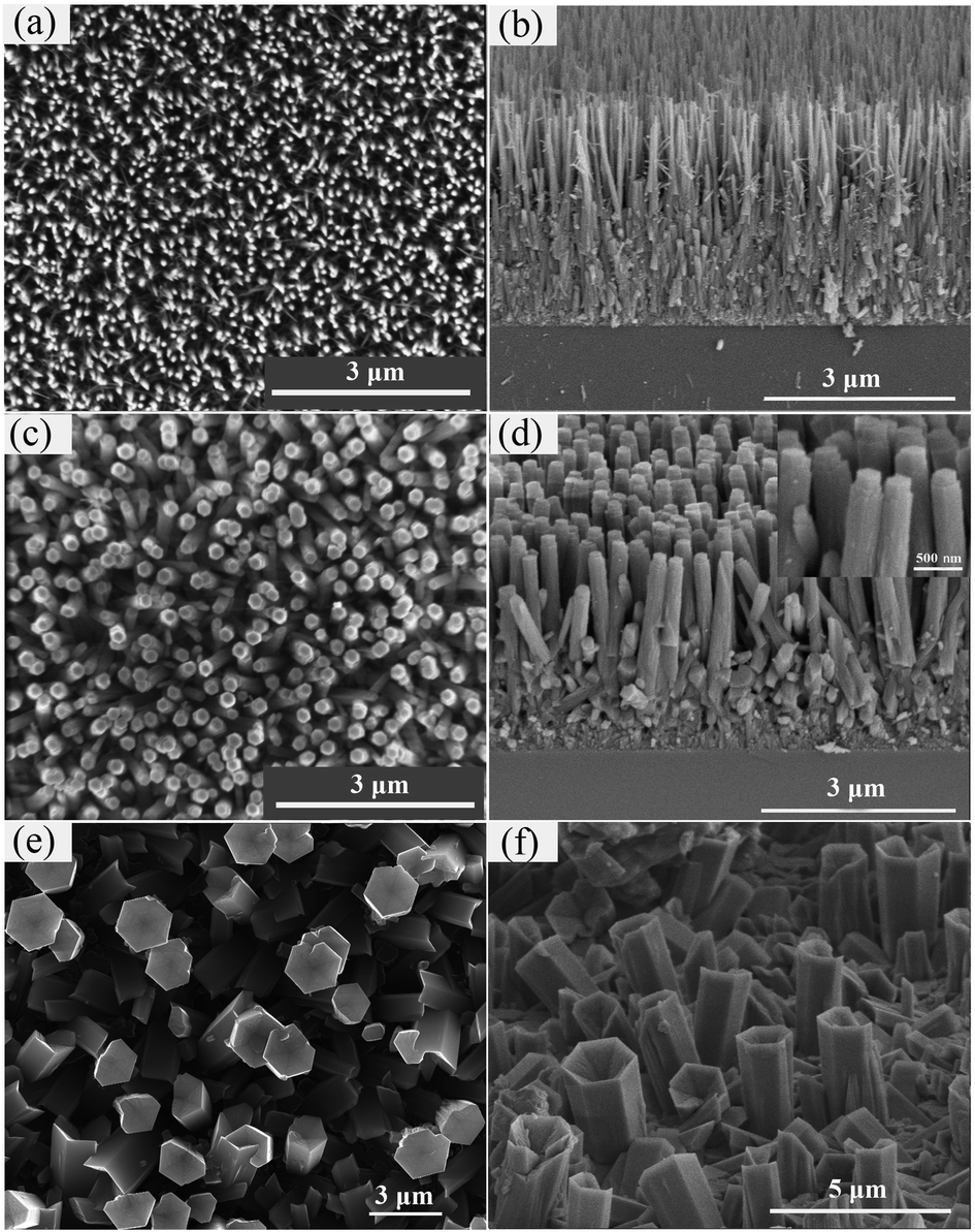 | ||
| Fig. 2 Typical SEM images of the AlN nanorods grown with temperature at (a) and (b) 750 °C, (c) and (d) 800 °C, (e) and (f) 900 °C, respectively. Inset in (d) is an enlarged image of the top of AlN nanorods grown at 800 °C. | ||
The morphology of AlN nanorods was also affected by the V/III ratio. In our experiments, the flow rate of NH3 was increased to obtain different V/III. Fig. 3 reports the post-growth SEM images of AlN nanorods grown with different V/III ratio at 800 °C for 30 minutes. For high V/III ratios of 30 and 22.5, the diameter of AlN nanorods was larger than those grown with the V/III ratio of 15 (Fig. 3c). When the V/III was increased to 22.5, the average diameter of AlN nanorods was increased to 550 nm (Fig. 3a). For a further increase of the V/III to 30, the shape of AlN nanorods changed into hexagonal columns and was similar to the AlN nanorods grown at 900 °C except for much smaller diameter and higher density (Fig. 3b).
 | ||
| Fig. 3 SEM images of the AlN nanorods grown with V/III at (a) 22.5, (b) 30. | ||
As the diameter of AlN columns grown at 900 °C was micron level, we focus on the AlN nanorods grown at 750 °C and 800 °C, further structure characterization of the AlN nanorods was carried out by Raman spectroscopy and transmission electron microscope (TEM). The Raman spectrum of the AlN nanorods was recorded at room temperature using a 532 nm solid state laser as the excitation source. There are six Raman-active modes, A1 (TO), A1 (LO), E1 (TO), E1 (LO), E2 (high) and E2 (low), in the first-order Raman scattering of wurtzite-type AlN. The E2 (high), E2 (low) and A1 (LO) are Raman-active modes in the backscattering configuration. However, other Raman modes may appear since not all the AlN nanorods were strictly vertical to the substrate.32 Fig. 4 is the Raman spectra of the AlN nanorods grown at 750 °C and 800 °C, the peaks located at 250, 613, 653 and 890 cm−1 can be assigned to E2 (low), A1 (TO), E2 (high) and A1 (LO), respectively. These are in agreement with those reported in the literatures.33,34
 | ||
| Fig. 4 Raman spectra of AlN nanorods grown at 750 °C and 800 °C. | ||
AlN nanorod with base diameter of 50 nm and apex diameter of 20 nm can be seen in Fig. 5a. Fig. 5b is the HRTEM image of one part of the nanorod. The interplanar spacing of 0.249 nm is in agree with those of (0002) plane of AlN. Low-magnification TEM image of AlN nanorod grown at 800 °C is shown in Fig. 6a, a decrease of diameter at the top of the rod can be seen, which is consistent with SEM image (Fig. 2d). The selected-area electron diffraction (SAED) pattern, which was taken along [010] zone axis, can be indexed as wurtzite-type hexagonal AlN and matches well with the corresponding HRTEM image (Fig. 6c). The interplanar spacing of (0001) and (100) planes is 0.499 nm and 0.269 nm, respectively. The results of Raman spectra and TEM indicate that the AlN nanorods grown at 750 °C and 800 °C are in good crystal quality and preferential grow along the [0002] direction.
 | ||
| Fig. 5 (a) TEM image, (b) corresponding HR-TEM image and the FFT pattern (inset) of one single AlN nanorod grown at 750 °C. | ||
 | ||
| Fig. 6 (a) TEM image, (b) SAED pattern, and (c) corresponding HR-TEM image and FFT pattern (inset) of one single AlN nanorod grown at 800 °C. | ||
In order to investigate the growth mechanism of the AlN nanorods, experiments were taken with different growth time at 800 °C with V/III of 15. The growth time was set at 30 seconds, 2 minutes, 5 minutes and 15 minutes, respectively. Fig. 7a is the cross-section SEM image of the AlN nanorods grown for 30 s, rod-like structures can be clearly seen even with such short time. That means AlN nanorods growth started at the initial stage of growth. Fig. 6b–d show the AlN nanorods grown for 2 min, 5 min and 15 min, respectively. When the growth time was increased, the length of nanorods increased roughly from 120 nm to 1.5 μm, while the diameter of nanorods only increased roughly from 30 nm to 135 nm.
 | ||
| Fig. 7 Typical SEM images of the AlN nanorods grown at 800 °C with growth time set at (a) 30 seconds, (b) 2 minutes, (c) 5 minutes, and (d) 15 minutes. | ||
As we did not apply Ni, Au or any other metal as catalyst in our experiment, the growth mechanism of AlN nanorods should be vapor–solid (VS) mechanism. Briefly, the gaseous source species transported to the surface of sapphire and reacted to form solid state AlN. Those solid state AlN absorbed onto the sapphire surface and AlN nucleus centers were then formed by the migration of those adatoms. According to van der Drift's evolutionary selection in growth orientation,35 [0002] direction, which is normal to the substrate, will survival during the competition with other growth directions, so the AlN nanorods grown along [0002] direction was preferential. Meanwhile, the strong covalent Al–N bonds restricted the migration of adatoms on the surface of substrate at low temperature, so the lateral growth of AlN nucleus and nanorods was restrained.36 Fig. 8 shows the growth rate of different directions as a function of the growth time at 800 °C. The feature sizes were determined from SEM measurements of the average diameter and length of AlN nanorods grown at different time. It's clearly shows that the vertical growth is far greater than lateral grow rate. AlN 1D nanostructures growth occurred with this anisotropic growth rate between vertical and lateral growth.
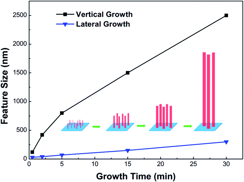 | ||
| Fig. 8 Growth rate of vertical and lateral direction as function of growth time. Inset is the schematic that illustrates the formation of AlN nanorods. | ||
The migration of adatoms is closely related to growth temperature, the surface diffusion length of adatoms, Ls, can be expressed as:

The supersaturation γ also plays an important role for the growth process. The supersaturation represents the progress of the reaction with respect to equilibrium.39 In the present investigations, supersaturation γ can be expressed as:

Conclusions
In conclusion, we report a fast and temperature controlled growth method of single crystal AlN nanorods. Well-aligned AlN nanorod arrays with preferential c-axis orientation have been successfully grown by HVPE without any catalyst or template. XRD, Raman and TEM results indicating AlN nanorods are single crystalline and in good crystal quality. With an increase in the growth temperature, AlN nanorods with different diameter and density have been grown. The increase of the diameter of AlN nanorods are due to the enhanced migration of adatoms at higher temperature. The morphology of AlN nanorods was also affected by V/III, high V/III is beneficial for lateral growth in our experiments. Different stages of the growth was discussed. It was found that the vertical growth rate was far great than the lateral growth. A VS growth model with anisotropic growth rate was proposed to explain the formation of AlN nanorods.Acknowledgements
This work was supported by National Nature Science Foundation of China (no. 91233111, 61274041 and 11275228), Special Funds for Major State Basic Research Project (973 program) of China (no. 2012CB619305), the 863 High Technology R&D Program of China (no. 2014AA032603), and Guangdong Provincial Special Fund for LED Industrial Development (no. 2012A080302003). The authors also appreciate Dalin Zhang for his technical support on SEM.Notes and references
- P. Y. Y. Xia, Y. Sun, Y. Wu, B. Mayers, B. Gates, Y. Yinl, F. Kim and H. Yan, Adv. Mater., 2003, 15, 353 CrossRef.
- S. Barth, F. Hernandez-Ramirez, J. D. Holmes and A. Romano-Rodriguez, Prog. Mater. Sci., 2010, 55, 563–627 CrossRef CAS PubMed.
- Z. L. Wang and J. H. Song, Science, 2006, 312, 242–246 CrossRef CAS PubMed.
- H. D. Espinosa, R. A. Bernal and M. Minary-Jolandan, Adv. Mater., 2012, 24, 4656–4675 CrossRef CAS PubMed.
- S. F. Li and A. Waag, J. Appl. Phys., 2012, 111, 071101 CrossRef PubMed.
- S. Nakamura, T. Mukai and M. Senoh, Appl. Phys. Lett., 1994, 64, 1687–1689 CrossRef CAS PubMed.
- S. J. Pearton, B. S. Kang, S. K. Kim, F. Ren, B. P. Gila, C. R. Abernathy, J. S. Lin and S. N. G. Chu, J. Phys.: Condens. Matter, 2004, 16, R961–R994 CrossRef CAS.
- S. Gradečak, F. Qian, Y. Li, H.-G. Park and C. M. Lieber, Appl. Phys. Lett., 2005, 87, 173111 CrossRef PubMed.
- S. Arafin, X. H. Liu and Z. T. Mi, J. Nanophotonics, 2013, 7, 074599 CrossRef PubMed.
- L. Liu and J. H. Edgar, Mater. Sci. Eng., R, 2002, 37, 61–127 CrossRef.
- M. Kasu and N. Kobayashi, Appl. Phys. Lett., 2000, 76, 2910 CrossRef CAS PubMed.
- G. Guisbiers and L. Buchaillot, J. Phys. D: Appl. Phys., 2008, 41, 172001 CrossRef.
- Q. Wang, Q. Sun, P. Jena and Y. Kawazoe, ACS Nano, 2009, 3, 621–626 CrossRef CAS PubMed.
- F. Liu, Z. J. Su, F. Y. Mo, L. Li, Z. S. Chen, Q. R. Liu, J. Chen, S. Z. Deng and N. S. Xu, Nanoscale, 2011, 3, 610–618 RSC.
- Z. Zhou, J. Zhao, Y. Chen, P. Schleyer and Z. Chen, Nanotechnology, 2007, 18, 424023 CrossRef PubMed.
- S.-C. Shi, S. Chattopadhyay, C.-F. Chen, K.-H. Chen and L.-C. Chen, Chem. Phys. Lett., 2006, 418, 152–157 CrossRef CAS PubMed.
- J. Yang, T. W. Liu, C. W. Hsu, L. C. Chen, K. H. Chen and C. C. Chen, Nanotechnology, 2006, 17, S321–S326 CrossRef CAS.
- X. Song, Z. Guo, J. Zheng, X. Li and Y. Pu, Nanotechnology, 2008, 19, 115609 CrossRef PubMed.
- F. Zhang, Q. Wu, X. Z. Wang, N. Liu, J. Yang, Y. M. Hu, L. S. Yu and Z. Hu, Vacuum, 2012, 86, 833–837 CrossRef CAS PubMed.
- J. Su, G. Cui, M. Gherasimova, H. Tsukamoto, J. Han, D. Ciuparu, S. Lim, L. Pfefferle, Y. He, A. V. Nurmikko, C. Broadbridge and A. Lehman, Appl. Phys. Lett., 2005, 86, 013105 CrossRef PubMed.
- V. Cimalla, C. Foerster, D. Cengher, K. Tonisch and O. Ambacher, Phys. Status Solidi B, 2006, 243, 1476–1480 CrossRef CAS.
- W. W. Lei, D. Liu, P. W. Zhu, Q. S. Wang, G. Liang, J. Hao, X. H. Chen, Q. L. Cui and G. T. Zou, J. Phys. Chem. C, 2008, 112, 13353–13358 CAS.
- Y. K. Byeun, R. Telle, S. H. Jung, S. C. Choi and H. I. Hwang, Chem. Vap. Deposition, 2010, 16, 72–79 CrossRef CAS.
- Q. Wu, Z. Hu, X. Z. Wang, Y. N. Lu, K. F. Huo, S. Z. Deng, N. S. Xu, B. Shen, R. Zhang and Y. Chen, J. Mater. Chem., 2003, 13, 2024–2027 RSC.
- Q. Zhao, H. Zhang, X. Xu, Z. Wang, J. Xu, D. Yu, G. Li and F. Su, Appl. Phys. Lett., 2005, 86, 193101 CrossRef PubMed.
- C. Liu, Z. Hu, Q. Wu, X. Wang, Y. Chen, H. Sang, J. Zhu, S. Deng and N. Xu, J. Am. Chem. Soc., 2005, 127, 1318–1322 CrossRef CAS PubMed.
- H. Cui, Y. Sun and C. X. Wang, CrystEngComm, 2013, 15, 5376 RSC.
- E. Nakamura, K. Ueno, J. Ohta, H. Fujioka and M. Oshima, Appl. Phys. Lett., 2014, 104, 051121 CrossRef PubMed.
- J. H. Choi, A. Zoulkarneev, S. I. Kim, C. W. Baik, M. H. Yang, S. S. Park, H. Suh, U. J. Kim, H. Bin Son, J. S. Lee, M. Kim, J. M. Kim and K. Kim, Nat. Photonics, 2011, 5, 763–769 CrossRef CAS.
- Y. Kumagai, T. Yamane, T. Miyaji, H. Murakami, Y. Kangawa and A. Koukitu, Phys. Status Solidi C, 2003, 2498–2501 CrossRef CAS.
- Y. S. Won, Y. S. Kim, O. Kryliouk and T. J. Anderson, J. Cryst. Growth, 2008, 310, 3735–3740 CrossRef CAS PubMed.
- T. Prokofyeva, M. Seon, J. Vanbuskirk, M. Holtz, S. Nikishin, N. Faleev, H. Temkin and S. Zollner, Phys. Rev. B: Condens. Matter Mater. Phys., 2001, 63, 125313 CrossRef.
- H. Harima, J. Phys.: Condens. Matter, 2002, 14, R967–R993 CrossRef CAS.
- J. G. Tischler and J. A. Freitas, Appl. Phys. Lett., 2004, 85, 1943 CrossRef CAS PubMed.
- A. Vanderdr, Philips Res. Rep., 1967, 22, 267–288 Search PubMed.
- J. Zheng, Y. Yang, B. Yu, X. B. Song and X. G. Li, ACS Nano, 2008, 2, 134–142 CrossRef CAS PubMed.
- Y. Kangawa, T. Akiyama, T. Ito, K. Shiraishi and T. Nakayama, Materials, 2013, 6, 3309–3360 CrossRef CAS PubMed.
- X. Q. Shen, H. Matsuhata, T. Ide and M. Shimizu, J. Appl. Phys., 2012, 111, 103529 CrossRef PubMed.
- K. Lekhal, G. Avit, Y. Andre, A. Trassoudaine, E. Gil, C. Varenne, C. Bougerol, G. Monier and D. Castelluci, Nanotechnology, 2012, 23, 405601 CrossRef CAS PubMed.
- A. Claudel, E. Blanquet, D. Chaussende, M. Audier, D. Pique and M. Pons, J. Cryst. Growth, 2009, 311, 3371–3379 CrossRef CAS PubMed.
| This journal is © The Royal Society of Chemistry 2014 |