 Open Access Article
 This Open Access Article is licensed under a
 Creative Commons Attribution 3.0 Unported Licence
Intrinsic electronic and transport properties of graphyne sheets and nanoribbons†
Wenzhi Wuab,
Wanlin Guo*a and
Xiao Cheng Zeng*b
aState Key Laboratory of Mechanics and Control of Mechanical Structures and Key Laboratory for Intelligent Nano Materials and Devices of MOE, Nanjing University of Aeronautics and Astronautics, Nanjing 210016, China. E-mail: wlguo@nuaa.edu.cn
bDepartment of Chemistry and Center for Materials & Nanoscience, University of Nebraska-Lincoln, Lincoln, Nebraska 68588, USA. E-mail: xzeng1@unl.edu
First published on 25th July 2013
Abstract
Graphyne, a two-dimensional carbon allotrope like graphene but containing doubly and triply bonded carbon atoms, has been proven to possess amazing electronic properties as graphene. Although the electronic, optical, and mechanical properties of graphyne and graphyne nanoribbons (NRs) have been previously studied, their electron transport behaviors have not been understood. Here we report a comprehensive study of the intrinsic electronic and transport properties of four distinct polymorphs of graphyne (α, β, γ, and 6,6,12-graphynes) and their nanoribbons (GyNRs) using density functional theory coupled with the non-equilibrium Green's function (NEGF) method. Among the four graphyne sheets, 6,6,12-graphyne displays notable directional anisotropy in the transport properties. Among the GyNRs, those with armchair edges are nonmagnetic semiconductors whereas those with zigzag edges can be either antiferromagnetic or nonmagnetic semiconductors. Among the armchair GyNRs, the α-GyNRs and 6,6,12-GyNRs exhibit distinctive negative differential resistance (NDR) behavior. On the other hand, the zigzag α-GyNRs and zigzag 6,6,12-GyNRs exhibit symmetry-dependent transport properties, that is, asymmetric zigzag GyNRs behave as conductors with nearly linear current–voltage dependence, whereas symmetric GyNRs produce very weak currents due to the presence of a conductance gap around the Fermi level under finite bias voltages. Such symmetry-dependent behavior stems from different coupling between π* and π subbands. Unlike α- and 6,6,12-GyNRs, both zigzag β-GyNRs and zigzag γ-GyNRs exhibit NDR behavior regardless of the symmetry.
1 Introduction
Carbon, the element providing the basis for most organic and biological molecules, has a broad range of unique chemical and physical properties largely due to possible formation of three distinct covalent bonds, namely, sp, sp2, sp3-hybridized bonds.1 In bulk crystalline form, carbon is known to possess three natural allotropes, i.e., cubic diamond, hexagonal diamond (lonsdaleite), and hexagonal graphite, which consist of extended networks of either sp3- or sp2-hybridized carbon atoms. These bulk-carbon allotropes show unique physical properties such as hardness,2 lubrication behavior,3 thermal conductivity4 and/or electrical conductivity.5 Conceptually, new carbon allotropes could be constructed via altering the periodic motif in their networks consisting of sp3-, sp2- and sp-hybridized carbon atoms. Over the past three decades, some low-dimensional carbon allotropes, such as fullerenes,6 carbon nanotubes,7 and graphene,8 have been successfully synthesized, which offer diverse and novel structural motifs for making high-performance carbon materials with new functionalities. Among them, graphene, a single atomic layer of sp2-bonded carbon, has been a central focus of carbon materials research for nearly a decade. Because of its single-atom thickness and highly symmetric network, graphene possesses some unusual properties. For example, its low-energy excitation spectrum with linear energy dispersion9,10 is contrary to the quadratic energy–momentum relationship observed in conventional semiconductors. This is because electrons in graphene mimic the behavior of massless Dirac fermions.11,12 In addition, graphene possesses outstanding carrier mobilities of ∼20![[thin space (1/6-em)]](https://www.rsc.org/images/entities/char_2009.gif) 000 cm2 V−1 s−1,13,14 mean free paths on the order of micrometer at room temperature,13 and conductivity approaching the ballistic value on the order of e2/h,13,15 all rendering graphene a highly attractive material for future applications such as electronics. Moreover, graphene can be patterned via the lithographic technique into quasi-one-dimensional (1D) graphene nanoribbons (GNRs) with added electronic and magnetic properties.16–23 In particular, zigzag-edged GNRs (ZGNRs) are predicted to be antiferromagnetic (AFM) semiconductors.17 Such zigzag edges can also give rise to other unusual properties such as half metallicity,18 magnetoelectric effect,20 and symmetry-dependent transport properties.24
000 cm2 V−1 s−1,13,14 mean free paths on the order of micrometer at room temperature,13 and conductivity approaching the ballistic value on the order of e2/h,13,15 all rendering graphene a highly attractive material for future applications such as electronics. Moreover, graphene can be patterned via the lithographic technique into quasi-one-dimensional (1D) graphene nanoribbons (GNRs) with added electronic and magnetic properties.16–23 In particular, zigzag-edged GNRs (ZGNRs) are predicted to be antiferromagnetic (AFM) semiconductors.17 Such zigzag edges can also give rise to other unusual properties such as half metallicity,18 magnetoelectric effect,20 and symmetry-dependent transport properties.24
The discovery of graphene-based two-dimensional (2D) carbon materials has sparked considerable research interest in finding new 2D carbon allotropes, especially 2D graphyne and graphdiyne.25–27 Like graphene, graphyne is also a one-atom-thick sheet of carbon atoms but with both sp and sp2 hybridized carbon bonds. The presence of the sp carbon atoms disintegrates the original honeycomb lattice of graphene. As a result, multiple lattice types of graphyne with different geometry arise. More specifically, four different types of graphyne, namely α-, β-, γ-, and 6,6,12-graphynes25,28 have been identified, each with different percentage of acetylenic linkages, i.e., 100%, 66.67%, 33.33%, and 41.67%, respectively. Despite the similarity between graphene and graphyne in topology, graphynes exhibit rich physical properties that are quite different from those of graphene due to the presence of the acetylenic linkages. Previous first-principles electronic structure calculations28–30 have shown that graphynes exhibit small carrier effective masses and high carrier mobility like graphene, and α-, β-, and 6,6,12-graphynes also possess Dirac cone-like band structures at the Fermi level,28 regardless of the existence or absence of the hexagonal (p6m) symmetry. Furthermore, two 6,6,12-graphyne derivatives,33 namely, 6(H2),14,18-graphyne and 6BN,6,12-graphyne, which contain either the heteroatom hydrogen or boron and nitrogen, are shown to entail Dirac points in their band structures. However, the single-layered γ-graphyne is predicted to be semiconducting with a direct band gap at the M point29–32 (the computed gap value ranging from 0.46 to 1.22 eV, depending on the exchange–correlation functional), and the band gap can be continuously tuned by the in-plane strain.30 Moreover, novel optical properties for this new class of 2D carbon nanostructures are predicted,30 including high third-order nonlinear optical susceptibility, strongly anisotropic optical absorption, and high fluorescence efficiency. Previous theoretical studies have also shown intriguing mechanical properties of graphynes. For example, graphynes soften significantly with the increasing temperature, a property completely different from that of the graphene because graphene can maintain its robust mechanical properties even at high temperatures.34 Also, the presence of the acetylenic linkages in graphynes results in significant reduction in fracture stress and Young's modulus, with the degree of reduction proportional to the percentage of the linkages.35 Among the four different graphynes, 6,6,12-graphyne exhibits exceptional directional anisotropy in its mechanical properties.35 Compared to theoretical studies on graphynes, less experimental studies have been reported in the literature due largely to the unavailability of free-standing graphynes in the laboratory. To our knowledge, only a few synthetic studies of graphdiyne films27 and nanoribbons36 have been reported.
On graphyne nanoribbons (GyNRs), previous theoretical studies have predicted electronic and magnetic properties of α- and γ-GyNRs.37,38 It is found that all the armchair-edged α-GyNRs (α-AGyNRs) are nonmagnetic semiconductors with their band gaps dependent on the ribbon widths. Moreover, the three families of α-AGyNRs can be classified according to their band gaps. The zigzag-edged α-GyNRs (α-ZGyNRs) are predicted to be AFM semiconductors, where the polarized electron spins are ferromagnetically aligned along the ribbon edges but antiferromagnetically coupled between the two opposite edges. As such, half-metallicity may be realized by applying a transverse electric field. In contrast, all the γ-GyNRs are semiconductors. The band gaps are located at the X point and decrease with the increasing width of nanoribbons. Interestingly, the band gap of zigzag γ-GyNRs (γ-ZGyNRs) shows a unique “step effect” as the width increases. These remarkable properties of graphynes afford their potential applications in optoelectronic devices, sensors, or energy storage.
To date, most previous studies have focused mainly on the electronic, optical, and mechanical properties of graphynes and their GyNRs. To our knowledge, little attention has been paid to the effect of acetylenic linkages on the electron transport properties and current–voltage (I–V) characteristics of graphyne and GyNRs. In this study, we perform a systematic investigation on the transport properties and current–voltage (I–V) characteristics of a variety of 2D graphyne sheets and 1D GyNRs, using the state-of-the-art first-principles quantum transport calculations. We show that the graphynes and their NRs exhibit many unique electronic, magnetic and transport properties very different from those of GNRs and boron-nitride (BN) NRs. We find that all armchair-edged GyNRs (AGyNRs) are nonmagnetic semiconductors, while all the zigzag-edged GyNRs (ZGyNRs) are magnetic semiconductors with the AFM ground state except that the γ-ZGyNRs can be either nonmagnetic or magnetic semiconductors. More interestingly, α-AGyNRs, armchair-edged 6,6,12-GyNRs (6,6,12-AGyNRs), zigzag-edged β-GyNRs (β-ZGyNRs), and γ-ZGyNRs all exhibit distinct negative differential resistance (NDR) effects, whereas the α-ZGyNRs and 6,6,12-ZGyNRs exhibit symmetry-dependent transport properties.
2 Computational method
Geometry relaxations and electronic structure calculations are based on density functional theory (DFT) as implemented in the SIESTA package.39 The generalized gradient approximation (GGA) within the Perdue–Burke–Ernzerhof (PBE) functional40 is used to treat the exchange–correlation potential, and the norm-conserving Troullier–Martins pseudopotentials41 are used for the core–valence interactions. The double-ζ polarized numerical atomic-orbital sets for C and H are selected along with the DFT calculations. Edges of all nanoribbons are saturated with hydrogen atoms to eliminate dangling bonds. The structures are fully relaxed using a conjugate gradient method with residual forces on each atom less than 0.01 eV A−1. An energy cutoff of 300 Ry is chosen and the vacuum layers are at least 15 Å in the non-periodic directions which is large enough to neglect interactions with their periodic replicas. The convergence criterion for the density matrix is chosen to be 10−4. The Brillouin-zone sampling of the calculations is determined after extensive convergence analysis.
The zero-bias conductance, bias-dependent electron transmission and current of graphyne sheets and NRs are computed using the non-equilibrium Green's function (NEGF) method based on the Keldysh formalism, as implemented in the Transiesta program package.42,43 The current through the contact region is calculated according to the Landauer–Büttiker formula44
| I = G0∫T(E, Vb)[fL(E) − fR(E)]dE |
3 Results and discussion
3.1 Electronic and transport properties of hexagonal α-graphyne sheet
We first optimize the structure of a 2D α-graphyne sheet, as shown in Fig. 1(a). Like graphene, the geometric structure of the α-graphyne sheet exhibits hexagonal lattice symmetry (p6m). The optimized lattice constant is 6.97 Å and the C1–C2 (C3–C4) bond length is 1.397 Å, while the C2–C3 bond length is 1.23 Å, close to the C![[triple bond, length as m-dash]](https://www.rsc.org/images/entities/char_e002.gif) C triple bond. These results are in agreement with previous calculations.38 The electronic band structure of the α-graphyne sheet is shown in Fig. 1(c). We can see that the valence and conduction bands cross a single point at the Fermi level, showing the Dirac-cone-like features like graphene, again consistent with the previous DFT results.28
C triple bond. These results are in agreement with previous calculations.38 The electronic band structure of the α-graphyne sheet is shown in Fig. 1(c). We can see that the valence and conduction bands cross a single point at the Fermi level, showing the Dirac-cone-like features like graphene, again consistent with the previous DFT results.28
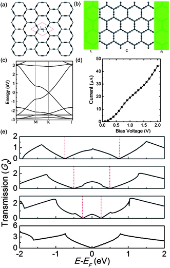 | ||
| Fig. 1 (a) Atomic structure and (b) schematic view of a two-probe α-graphyne sheet. (c) Band structure of the monolayer α-graphyne sheet. (d) Computed I–Vb curve of the α-graphyne sheet based device shown in (b). (e) Computed transmission spectra for 0, 0.5, 1.0, and 1.5 V bias voltages (listed from bottom to top), respectively. The rhombus in (a) represents a unit cell of the α-graphyne sheet and the dashed lines in (e) indicate the bias windows. The gray balls in (b) denote carbon atoms. | ||
Based on the optimized structures, we next investigate the electron transport properties of the 2D α-graphyne sheet by constructing a two-probe system, as shown in Fig. 1(b), where the central scattering region of the α-graphyne sheet is sandwiched between semi-infinite left- and right-electrodes. Both electrodes and the central region are made of the 2D α-graphyne sheet. The transmissions are given in the zigzag direction. Periodic boundary conditions are imposed on the plane perpendicular to the transport direction. The computed zero-field transmission spectrum is shown in Fig. 1(e), which apparently mimics the metallic band structure of the α-graphyne sheet. The current as a function of the applied bias voltage Vb is presented in Fig. 1(d). Here it should be noted that we increase Vb in steps of 0.1 V and use the converged density matrix of the previous state as an initial guess for the next step. It is found that the 2D α-graphyne sheet shows metal-like conduction, consistent with the zero-field transmission spectrum shown in Fig. 1(e). To understand the monotonic increase of the current with the increasing applied bias voltage, we present the evolution of the transmission spectra with bias voltages in Fig. 1(e). At zero bias, there is no transmission arising from the zero-gap band structure of the α-graphyne sheet. As the bias voltage increases, the valence band (π band) in the left electrode and the conduction band (π* band) in the right electrode overlap within the bias window (see ESI, Fig. S1†), which allows the electrons in the valence band of the left electrode to be transmitted to the conduction band of the right one. Thus a transmission peak arises around the Fermi level as shown in Fig. 1(e) and the transmission coefficient in the bias window increases steadily with the increasing bias voltage. As a result, the current, determined by the integral of T(E, Vb) over the bias window [−eVb/2, eVb/2] based on the Landauer–Büttiker formula, increases monotonically with the increasing bias voltage.
3.2 Electronic and transport properties of armchair and zigzag α-graphyne NRs
We now report computed structural and electronic properties of α-GyNRs. Similar to GNRs, the α-GyNRs exhibit two typical edge structures, namely, armchair and zigzag, for which the corresponding nanoribbons are denoted as α-AGyNRs and α-ZGyNRs, respectively. Both nanoribbons can be cut out from a single-layer h-α-graphyne sheet along the respective crystallographic orientations. Following the convention, we use the notation N-α-AGyNR to describe an α-AGyNR having N number of C dimer lines across the ribbon width and use N-α-ZGyNR to describe an α-ZGyNR having N zigzag C chains, as shown in Fig. 2(a) and 3(a), respectively. We terminate all the edge C atoms with H atoms to remove the effect of dangling bonds. | ||
| Fig. 2 (a) Atomic structure and (b) schematic view of a two-probe α-AGyNR device. (c) Band structure of 6-α-AGyNR in its primitive unit cell. (d) The variation of current as a function of bias voltage for 6-, 7-, and 8-α-AGyNRs. (e) The transmission spectra for 0.9, 1.2, 1.4, and 1.5 V bias voltages (from bottom to top), respectively. The dashed lines in (e) indicate the bias windows. The gray and white balls in (a) and (b) denote C and H atoms, respectively. | ||
 | ||
| Fig. 3 Atomic structure of (a) asymmetric 5-α-ZGyNR and (b) symmetric 6-α-ZGyNR, with the mirror plane σ denoted by the solid blue line. The dashed rectangle denotes the unit cell of the α-ZGyNR. (c) Computed I–Vb curves for 5- and 6-α-ZGyNR devices shown in the inset of (b). (d) Computed transmission spectra for 4-, 5-, and 6-α-ZGyNRs (from left to right) under 0.5 V bias voltage, respectively. | ||
It has been reported that all the α-AGyNRs are nonmagnetic semiconductors with band gaps depending on the ribbon width (namely, N).38 The α-AGyNRs can be grouped into three families with N = 3p, 3p + 1, 3p + 2, where p is a positive integer. And the gaps have a hierarchy as Δ3p+1 > Δ3p > Δ3p+2. The α-ZGyNRs have a magnetic semiconducting ground state with ferromagnetic ordering at each edge and opposite spin orientation between the two edges.38 In the following sections we will first present the transport properties of α-AGyNRs, and then those of α-ZGyNRs.
First, the band structures of the electrodes and the scattering region in their primitive unit cells are shown in Fig. 2(c), which can provide an understanding of the transport phenomena. It is found that the 6-α-AGyNR is a semiconductor with a direct band gap of 0.418 eV. The lowest conduction and the highest valence bands originate from π* and π band states, respectively. Next, the I–Vb curve of the two-probe device is computed (see Fig. 2). Clearly, the I–Vb characteristic is semiconducting, corresponding to the energy band structure shown in Fig. 2(c). The system has a threshold voltage Vth ≈ 0.4 V, below which the current is always close to zero, and above which the current begins to increase. More interestingly, the negative differential resistance (NDR) behavior can be observed with a peak–valley ratio (PVR) of 1.4. Here the PVR is defined as the ratio of the peak current Ip to the valley current Iv.
To understand the semiconducting I–Vb characteristic and the mechanism of the NDR effect observed, the transmission spectra are presented in Fig. 2(e). By applying a bias voltage the Fermi level of the left electrode shifts with respect to the Fermi level of the right electrode. At zero bias, there is a conductance gap (Cgap) of about 0.4 eV owing to the energy gap of 6-α-AGyNR. As the bias increases, the energy bands of the electrodes shift with the corresponding chemical energies and mismatch with one another so that the conductance gap becomes wider (see ESI, Fig. S2†). Furthermore, the conductance gap increases linearly with increasing bias voltage (see ESI, Fig. S2d†). When the bias increases further beyond 0.4 V, the threshold voltage, the valence band of the left electrode matches well in energy with the bottom of the conduction band of the right electrode. As a result, the electrons can tunnel through from the valence band of the left electrode to the conduction band of the right electrode, and thus the transmission coefficient becomes finite in the middle of the transport window as shown in Fig. 2(e), hence the current flows. Moreover, the transmission coefficient increases with the increasing bias voltage in the range of 0.4–1.2 V, which leads to the monotonic current increase in this bias window. When the bias is between 1.2 V and 1.4 V, the NDR behavior is observed with a dip in the current–voltage curve (Fig. 2(d)). As shown in Fig. 2(e), the transport window widens from [−0.6, 0.6] eV to [−0.7, 0.7] eV when the bias voltage increases from 1.2 to 1.4 V. Although the range of transport window with a nonzero transmission coefficient widens from [−0.42, 0.46] eV to [−0.47, 0.5] eV, the transmission coefficient decreases in the middle of the transport window, resulting in a decrease of the current and thus the NDR behavior at bias 1.4 V, as illustrated in Fig. 2(d).
For comparison, the I–Vb characteristics of 7- and 8-α-AGyNRs are also presented in Fig. 2(d). The 7-α-AGyNR belongs to the N = 3p + 1 family and possesses a slightly wider band gap (0.425 eV) compared to the 6-α-AGyNR (0.418 eV). As a result, the current is not observed until 0.425 eV as can be seen from Fig. 2(d). In contrast, the 8-α-AGyNR, belonging to the N = 3p + 2 family, yields a higher current at the same bias voltage, owing to its band structure with a band gap of ∼20 meV which is much narrower than that of 6- or 7-α-AGyNRs. Clearly, a NDR peak appears in all cases. For example, the PVR is up to about 1.9 and 1.1 for 7- and 8-α-AGyNRs, respectively.
We take 5- and 6-α-ZGyNRs as two prototypes to represent odd-N and even-N α-ZGyNRs, respectively (see Fig. 3(a) and (b)). There exists mirror reflection symmetry, described by a single mirror-symmetry plane σ, for the symmetric 6-α-ZGyNRs but not for the asymmetric 5-α-ZGyNRs. To compute the current–bias voltage (I–Vb) curves of the α-ZGyNRs, we construct two-probe systems as shown in the inset of Fig. 3(c) using either 5- or 6-α-ZGyNRs. The two-probe system contains a scattering region consisting of three primitive unit cells with the length of 20.91 Å, and two (left and right) semi-infinite α-ZGyNR electrodes. Fig. 3(c) shows the computed I–Vb curve for the two-probe device. Like ZGNRs, the symmetric and asymmetric α-ZGyNRs do exhibit very different transport characteristics. The 5-α-ZGyNR behaves like a conductor and the current increases linearly with increasing bias within a finite voltage range. As shown in Fig. 3(d), this characteristic arises from the presence of one conductance quantum (G0) around the Fermi level. On the other hand, the 6-α-ZGyNR shows very low currents (close to zero) when Vb is less than a critical bias voltage (Vc). Beyond Vc the current begins to increase due to the presence of a conductance gap (Cgap) around the Fermi level. Moreover, the conductance gap increases linearly with the increasing bias voltage (see ESI, Fig. S3†) and is slightly narrower than the bias window (eVb). The computed I–Vb curve and transmission spectrum of 4-α-ZGyNR, as shown in Fig. 3(c) and 3(d), respectively, reconfirm that symmetric α-ZGyNRs do exhibit very different transport characteristics from asymmetric ones.
We next investigate the underlying mechanism governing the symmetry-dependent transport behavior of α-ZGyNRs. In general, distinct transport behaviors are correlated with characteristics of the electronic band structures. The band structures of 5- and 6-α-ZGyNRs are plotted in Fig. 4(a) and (b), respectively. However, both α-ZGyNRs appear to exhibit very similar band structures, consistent with previous studies.38 Consequently, the distinct transport behavior of α-ZGyNRs must stem from special characteristics other than the band structures. In addition to the similarity in band structures, we can see that around the Fermi level, the peculiar degenerate flat edge states hybridize to form bonding and antibonding states, i.e., π and π* subbands when spins are not considered. We thus can expect that the characteristics of the π and π* subbands would dictate the electron transmission under low bias. As shown in Fig. 4(b) and (d), the Γ-point wave functions of the π and π* subbands do exhibit different characteristics. The wave functions present a well-defined parity with respect to this symmetry plane in which π*(π) subbands have odd (even) parities under σ mirror operation for symmetric 6-α-ZGyNRs, while for asymmetric 5-α-ZGyNRs both subbands have no definite parity due to the lack of the mirror plane.
 | ||
| Fig. 4 (a) Band structure around the Fermi level and (b) Γ-point wave functions of π and π* subbands for 5-α-ZGyNR. (c) Band structure around the Fermi level and (d) Γ-point wave functions of π and π* subbands for 6-α-ZGyNRs. (e) Band structures for the left and right electrodes, and the transmission spectrum of 5-α-ZGyNRs under 0.4 V bias voltage (highlighted by the green bar). (f) Band structures for the left and right electrodes, and the transmission spectrum of 6-α-ZGyNR under 0.4 V bias voltage. The yellow and blue colors indicate opposite signs of the wave function. | ||
To analyze symmetry-dependent transport behaviors of the α-ZGyNRs, we present some details of the transmission spectrum and band structures of left and right electrodes for 5- and 6-α-ZGyNRs. When a bias voltage is applied, the chemical potentials of left and right electrodes (uL and uR) are separated by eVb. Only the electrons in the states between uL and uR can contribute to the current. As shown in Fig. 4, when eVb < Δ, only the π subband of the left electrode overlaps with the π* subband of the right electrode within the bias window. For symmetric 6-α-ZGyNRs, due to the opposite parity of π and π* subbands under the σ mirror operation, the hopping integral is zero, and consequently the electrons cannot hop from the π subband of the left electrode to the π* subband of the right electrode, leading to a conductance gap appearing around the Fermi level and thereby a very low current. On the other hand, for the asymmetric 5-α-ZGyNR, the hopping integral is nonzero due to the lack of the mirror plane σ, and therefore the electrons can hop from the π subband of the left electrode to the π* subband of the right electrode and contribute to the transmission. Correspondingly, the 5-α-ZGyNR maintains a G0 conductance within the bias windows. When eVb > Δ, the other energy bands begin to contribute to the conductance and thus the currents through α-ZGyNRs increase with the increasing bias voltage.
3.3 Electronic and transport properties of hexagonal β-graphyne sheet
Like graphene and α-graphyne sheets, the atomic structure of a β-graphyne sheet also exhibits hexagonal lattice symmetry (p6m). The optimized structure is shown in Fig. 5(a). The optimized lattice constant is 9.48 Å, the C1–C2 bond length is 1.46 Å, the C3–C4 bond length is 1.23 Å, close to the CC triple bond, and the C5–C6 bond length is 1.39 Å, in agreement with previous calculations.25 The calculated electronic band structures of the β-graphyne sheet are shown in Fig. 5(c). Our calculation confirms that β-graphyne possesses the Dirac cone which occurs at the low-symmetry points, contrary to graphene and α-graphyne.
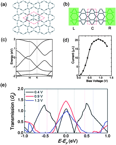 | ||
| Fig. 5 (a) Atomic structure of a 2D β-graphyne sheet and (b) schematic structure of the two-probe β-graphyne device. (c) Computed electronic band structures of a β-graphyne sheet. (d) The current versus the bias voltage (I–Vb) curve for the system shown in (b). (e) Transmission spectra of a β-graphyne device under a bias of 0.4, 0.9 and 1.3 eV, respectively. The dashed rectangle in (a) and rhombus in (b) denote the unit cell. The vertical lines in (e) indicate the bias windows. | ||
To compute electron transport properties of the 2D β-graphyne sheet, the two-probe system is still used as shown in Fig. 5(b). The transmission is in the armchair direction. The scattering region contains three primitive unit cells with the length of 28.43 Å. The computed current versus the bias voltage (I–Vb) curve is shown in Fig. 5(d). Similar to α-graphyne, the I–Vb characteristics for β-graphyne is metallic, consistent with the energy band structures. Moreover, the NDR effect is observed for the β-graphyne.
To understand the physical origin of the NDR in β-graphyne, we inspect the transmission spectra at three typical biases as illustrated in Fig. 4(e). As we all know, the current within the bias window is determined by the integration of T(E, Vb) over the interval −eVb/2 ∼ eVb/2. At zero bias, there is no transmission at the Fermi energy (not shown here) due to the metallic band structure. As the bias voltage increases, some features of the transmission function change dramatically. A transmission peak arising from the overlap of the valence band in the left electrode and the conduction band in the right electrode is observed around the Fermi level within the bias window. Thus the current arises. In more detail, compared to the case of 0.4 eV bias, the bias window is wider and the transmission coefficient becomes larger than 0.9 eV, resulting in a notable increase in the current. In contrast, the transmission coefficient decreases markedly with the increasing bias voltage to 1.3 eV, giving rise to a dip in the current and the NDR effect.
3.4 Electronic and transport properties of armchair and zigzag β-graphyne NRs
Here two typical patterns of the 1D β-GyNRs with the armchair and zigzag edges are denoted as β-AGyNRs and β-ZGyNRs. As shown in Fig. 6(a) and 7(a), the size of the unit cells of β-GyNRs is indexed by the number N. For simplicity, we use the notation N-β-AGyNRs or N-β-ZGyNRs to represent β-GyNRs with different widths. The dangling bonds at the edges are saturated with H atoms. The optimized structure of the 2-β-AGyNR is shown in the ESI, Fig. S4.† To determine the ground state of β-AGyNRs, we perform total energy calculations for spin-unpolarized and spin-polarized states, respectively. No energy difference is seen between the two states, indicating that the A-β-graphyne NRs are nonmagnetic (NM). The band structure of 2-β-AGyNR is plotted in Fig. 6(b). A band gap of 0.13 eV at the Γ point is found between the valence-band maximum (VBM) and the conduction-band minimum (CBM). The variation in the band gap Eg of the β-AGyNRs as a function of ribbon width (namely, N) is shown in Fig. 6(c), where the band gap decreases with increasing N, contrary to the case of AGNRs and α-AGyNRs where three distinct behaviors can arise. | ||
| Fig. 6 (a) Atomic structure of 1D armchair β-GyNRs. (b) Computed band structure of 2-β-AGyNR. (c) The variation in the band gap Eg of the β-AGyNRs as a function of ribbon width. (d) The I–Vb curve and (e) the transmission spectrum at the zero-bias voltage for the two-probe 2-β-AGyNR device. | ||
We next investigate the structural and electronic properties of β-ZGyNRs, taking the 4- and 5-β-ZGyNR as two prototype models. Total-energy calculations are performed for the β-ZGyNR in the ferromagnetic (FM) state, AFM state, and NM state, respectively. The relative energies among FM, AFM, and NM states are shown in the ESI, Table S1.† We find that the AFM state is the ground state as the total energy is lower than the NM state by 9 meV per supercell for 4-β-ZGyNRs and 44.7 meV per supercell for 5-β-ZGyNRs. The band structures in the NM state of the 4- and 5-β-ZGyNR are displayed in Fig. 7(c). It is found that 4-β-ZGyNR exhibits semiconducting behavior with a band gap of 0.04 eV. For 5-β-ZGyNR, around the Fermi level, there are two near-degenerate subbands which meet at the X point in the first Brillouin zone, while the nearly flat bands seen for ZGNRs and α-ZGyNRs (see Fig. 4(a)) are not observed for β-ZGyNRs. Note that the flat bands seen in ZGNRs and α-ZGyNRs are mainly due to the edge states. Consequently, the absence of flat bands for β-ZGyNRs suggests that their edge magnetism differs from those of ZGNRs and α-ZGyNRs. To address this issue, we perform further calculation of the spin-polarized band structure of 5-β-ZGyNR. Fig. 7 presents the band structures for the AFM state. The states of opposite spin orientation are degenerate in all bands, and a band gap of 0.24 eV is observed around the Fermi level. We then plot the spatial spin-density distribution for the ground state of the 5-β-ZGyNR. The spin density is distributed over the entire nanoribbon which is markedly different from those of ZGNRs and α-ZGyNRs where a rapid decay from the ribbon edge to the interior is observed for these states. The distinct spin-density distribution can be attributed to the absence of flat bands in β-ZGyNRs. We also carry out extensive computation of the band structures for a series of N-β-ZGyNRs and find that the β-ZGyNRs with N > 5 have similar electronic properties to 5-β-ZGyNR.
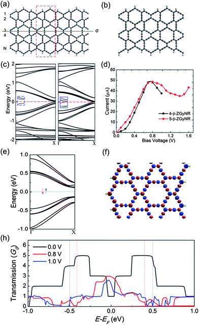 | ||
| Fig. 7 Atomic structure of (a) symmetric and (b) asymmetric β-ZGyNRs. The band structures for (c) the NM state of 4- and 5-β-ZGyNRs and (e) the AFM state of 5-β-ZGyNR. (d) The computed I–Vb curve and (f) spatial spin-density distribution (ρ↑ − ρ↓) with an iso-surface value of 0.002 e Å−3 of the 5-β-ZGyNR. (h) The transmission spectra under the bias voltages of 0, 0.8 and 1.0 V, respectively. The solid blue line in (a) represents the mirror plane σ, and the dashed red rectangle denotes the unit cell. | ||
To elucidate the NDR mechanism, some details of the transmission functions are presented in Fig. 7. It is clear that 5-β-ZGyNRs have a non-negligible transmission at the Fermi energy at zero bias, which is different from the case of α-ZGyNRs. With an increase in the bias voltage to 0.8 V, the bias windows and the transmission increase simultaneously, resulting in the increase of the current. When the bias is further increased to 1.0 V the transmission decreases in the middle of the transport window, leading to the NDR behavior.
3.5 Electronic and transport properties of hexagonal γ-graphyne sheet
The optimized geometric structure of a 2D γ-graphyne sheet is shown in Fig. 8(a). The optimized lattice constant is 6.89 Å. The C1–C2 bond length is 1.426 Å, the C3–C4 bond length is 1.223 Å, close to the CC triple bond, and the C5–C6 bond length is 1.408 Å, in agreement with previous calculations.29,30,37 The band structures of γ-graphyne were calculated by Narita et al.29 using LDA, which exhibit a direct band gap of 0.52 eV. The effective masses of the carriers in γ-graphyne are anisotropic. Kang et al.30 also calculated the band structures using the GGA-PBE method, and obtained similar band structures and the band gap of 0.46 eV. They also confirmed that the effective masses of carriers in γ-graphyne are anisotropic although the values are different. Our calculated band structures of γ-graphyne are shown in Fig. 8(b), and the band gap is 0.49 eV, consistent with previous results.29,30,37
 | ||
| Fig. 8 (a) Computed atomic and (b) band structures of a 2D γ-graphyne sheet. (c) The transmission spectrum of the γ-graphyne sheet under zero-bias voltage. (d) The I–Vb curve of a two-probe γ-graphyne device under a bias voltage from 0 to 2.0 V. (e) The transmission spectrum under a bias voltage of 1.0, 1.5, 1.8 and 2.0 V, respectively, of a two-probe γ-graphyne device. The red dashed rhombus in (a) denotes the unit cell. | ||
Again, we compute transport properties of the 2D γ-graphyne sheet using the two-probe model. The transmissions are in the armchair direction. The transmission coefficient T(E, Vb) at zero bias (Vb = 0) is shown in Fig. 8(c). Note that the transport properties at zero bias play an important role at low bias. Clearly, one can see a transmission valley near the Fermi level, indicating the appearance of a conductance gap. Thus, at low bias, it is harder for electrons to transport through the scattering region. As a result, the 2D γ-graphyne displays semiconducting behavior as shown in Fig. 8(b).
To further understand the transport properties of the 2D γ-graphyne sheet, we compute the I–Vb characteristics for the two-probe device, as shown in Fig. 8(d). The I–Vb characteristics display the semiconducting behavior. There is a threshold voltage of ∼0.5 V below which the conductance gap increases with the increasing bias voltage due to the shift of the band structures (or density of states, see ESI, Fig. S5†) in the left and right electrodes. Below the threshold voltage, electron tunneling through the central scattering region from the left to the right electrode is not allowed, hence almost zero transmission. If the bias increases beyond 0.5 V, the valence band of the left electrode matches well with the conduction band of the right electrode. As a result, the electrons can hop from the valence band of the left electrode to the conduction band of the right one and thus the transmission becomes finite in the transport window. Consequently, the current becomes non-zero at high bias. Note that a weak NDR effect can be observed with dips in the current occurring between 1.5 and 1.8 V, which can be understood based on the transmission functions presented in Fig. 8(e). Let us focus on the transmission peak around the Fermi level because the current in the bias window is only contributed by the peak. When the bias voltage increases from 0.5 V to 1.5 V both the bias window and the transmission coefficient increase. Thus a dramatic increase in the current is resulted. Compared to the case of 1.5 V bias voltage, the bias window of 1.8 V bias voltage increases but the averaged transmission coefficient decreases, resulting in a drop in the current. The current increases again with the increase of the bias window, as demonstrated in Fig. 8(e) for 2.0 V, giving rise to the NDR effect with a small PVR of 1.04.
3.6 Electronic and transport properties of armchair and zigzag γ-graphyne nanoribbons
The structural and electronic properties of γ-GyNRs were investigated by Pan et al.37 They considered both armchair and zigzag nanoribbons, as shown in Fig. 9(a) and (b). The width of the γ-GyNRs is indexed by the number of repeating units N. Again, a 1D γ-GyNR is denoted as either N-γ-AGyNR or N-γ-ZGyNR. Note that N can differ by a half-integer in γ-ZGyNRs. Pan et al.37 found that all the γ-GyNRs exhibit semiconducting behavior with a band gap at the X point, regardless of their edges (see Fig. 9(e) and (f)). The band gaps decrease as the width of γ-GyNRs increases. In particular, the band gap of γ-ZGyNRs shows a unique “step effect” as the width increases. In addition to the γ-AGyNRs and γ-ZGyNRs reported by Pan et al.,37 we construct another configuration with the zigzag edge, denoted as N-γ-Z′GyNRs (see Fig. 9(c)). Both spin-unpolarized and spin-polarized computations are performed to determine the ground state of γ-Z′GyNRs. Computed relative energies among FM, AFM, and NM states are shown in the ESI, Table S1.† Clearly, the AFM state is the ground state of the γ-Z′GyNRs. The band structure in Fig. 9(g) shows that the NM state exhibits metallic behavior with a twofold degenerated flat edge band at the Fermi level, similar to the case of ZGNRs and α-ZGyNRs. The spin-polarized band structure of 6-γ-Z′GyNRs as well as the magnetization density (ρ↑ − ρ↓) iso-surface plot for the AFM state are shown in Fig. 9(h). The 6-γ-Z′GyNR in the AFM state exhibits a direct band gap of 0.40 eV with AFM coupling between two edges, each in the ferromagnetically ordered edge state. The magnetization undergoes a rapid decay from the ribbon edge to the interior. | ||
| Fig. 9 Optimized structures of (a) N-γ-AGyNRs where N denotes the number of chains of hexagonal carbon rings, (b) N-γ-ZGyNRs, and (c) N-γ-Z′GyNRs. The primitive unit cell is represented by a red dashed rectangle. (d) Spin density for 6-γ-Z′GyNR with an iso-surface value of 0.002 e Å−3. Band structures of (e) 4-γ-AGyNR, (f) 4-γ-ZGyNR, and 6-γ-Z′GyNR in (g) the NM state or (h) the AFM state. | ||
 | ||
| Fig. 10 (a) The I–Vb curves for 4-, 5-, and 6-γ-AGyNRs. (b) The transmission spectra for four different bias voltages, i.e., 0, 0.7, 1.0, and 1.4 V (from left to right). | ||
 | ||
| Fig. 11 (a) Schematic structure of the two-probe 5-γ-Z′GyNR device. (b) The variation of current as a function of bias voltage for 4-γ-ZGyNR, 4-γ-Z′GyNR and 5-γ-Z′GyNR. The transmission spectra for four different bias voltages: (c) 0, 0.7, 1.0, and 1.4 V for 4-γ-ZGyNR, and (d) 0.2, 0.3, 0.6, and 0.8 V for 5-γ-Z′GyNR. | ||
For 4-γ-ZGyNR, the current versus voltage curve (see Fig. 11(b)) exhibits the semiconducting behavior and the threshold voltage decreases with the increasing width of NR. The transmission spectra as a function of the electron energy and bias are plotted in Fig. 11(c). At a low bias, a wide conductance gap can be observed around the Fermi level and is broadened with the increase of bias. However, the conductance gap around the Fermi level is removed away from the Fermi level, and two wide conductance gaps are formed at both sides of the Fermi level and shifted away from the Fermi level with the increase of the bias.
For 4-γ-Z′GyNR and 5-γ-Z′GyNR, we focus on the spin-unpolarized metallic state on the basis of the same reason as for α-ZGyNRs. Note that the 4-γ-Z′GyNR is symmetric while the 5-γ-Z′GyNR is asymmetric. The current versus the bias is shown in Fig. 11(b), where both systems exhibit metallic behavior. The symmetry-dependent transport properties are not found. Moreover, NDR behavior can be seen for both systems, and the NDR appears at different bias for different widths. In addition, the dips in the current occur in different bias ranges for each γ-Z′GyNR. The PVR is up to about 13 and 2.4 for 4- and 5-γ-Z′GyNRs, respectively.
To understand the physical origin of the NDR in the γ-Z′GyNRs, the transmission spectra for 5-γ-Z′GyNR at four typical biases are shown in Fig. 11(d). The current is mainly contributed by the transmission coefficient within the bias window around the Fermi level. Compared to the case of 0.2 V bias, although the transmission coefficient is nearly the same, the integration bias range for 0.3 V is significantly enhanced, resulting in a dramatic increase in the current. However, the transmission coefficient in the bias window decreases considerably with the continuously increasing bias to 0.6 V, and this decrease causes a dip in current. The current then increases again with the increase of the transmission coefficient in the bias window, as demonstrated in Fig. 11(d) for 0.8 V bias, resulting in the NDR behavior.
3.7 Electronic and transport properties of hexagonal 6,6,12-graphyne sheet
The optimized structure is shown in Fig. 12(a). In contrast to graphene or α-graphyne or β-graphyne, the 6,6,12-graphyne exhibits rectangular (pmm) symmetry rather than hexagonal symmetry. Previous studies28 show that the 6,6,12-graphyne also exhibits Dirac-cone-like band structures around the Fermi level and the Dirac points do not appear at the K or K′ points in the Brillouin zone. More importantly, the 6,6,12-graphyne possesses direction-dependent electronic properties.28 The highly anisotropic electrical properties likely lead to anisotropic I–Vb characteristics for the 6,6,12-graphyne. | ||
| Fig. 12 (a) Optimized geometric structure and (b) the band structure of a 6,6,12-graphyne sheet. The red rectangle in (a) represents the primitive unit cell. Schematic structure of the two-probe systems, where the transport direction is (c) armchair and (d) zigzag, respectively, as marked by the red arrows. (e) Calculated I–Vb curves for the systems shown in (c) and (d). | ||
For computing the transport properties of the hexagonal 6,6,12-graphyne sheet, the two-probe models of 6,6,12-graphyne are shown in Fig. 12(c) and (d). The central region of 6,6,12-graphyne is sandwiched between semi-infinite 6,6,12-graphyne electrodes. The transport direction is armchair (denoted as A-6,6,12-sheet) as shown in Fig. 12(c) and zigzag (denoted as Z-6,6,12-sheet) as shown in Fig. 12(d). Fig. 12(e) shows the I–Vb curve of the 6,6,12-graphyne, based on the Landauer–Büttiker formula. Indeed, the 6,6,12-graphyne exhibits highly anisotropic electrical transport properties even though both systems are metallic. For the A-6,6,12-sheet, the current increases monotonously with the increasing bias voltage and tends to level off at voltages above 0.7 V, while for the A-6,6,12-sheet, the current keeps increasing as the bias voltage increases. The current in A-6,6,12-sheet is higher than in Z-6,6,12-sheet when the bias voltage is between 0 and 0.4 V. The case reverses when the bias voltage is >0.4 V. To understand the origin of fascinating electrical transport properties of 6,6,12-graphyne, we compute electronic band structures in the periodic central region (in the NEGF model shown in Fig. 12). As Daniel Malko et al.28 reported previously, the bands in the kx and ky directions show different slopes and curvatures, which result in different shapes of the two Dirac cones due to the rectangular symmetry of 6,6,12-graphyne. The rectangular symmetry, along with the distortion of the Dirac cones with different slopes and curvatures at the Dirac points in the kx and ky directions, gives rise to the direction-dependent electronic conductivities.
3.8 Electronic and transport properties of armchair and zigzag 6,6,12-graphyne NRs
Here, the N-6,6,12-AGyNR denotes a 6,6,12-AGyNR with N benzene rings in the unit cell, while the N-6,6,12-ZGyNR denotes a 6,6,12-ZGyNR with N zigzag chains along the longitudinal direction. Our calculations show that 6,6,12-AGyNRs are nonmagnetic semiconductors. Fig. 13(a) and (b) show the atomic and electronic structures of 3-6,6,12-AGyNR. Both VBM and CBM are located at the Γ point with an energy gap of 0.12 eV. The variation in the energy gap (Eg) of the 6,6,12-AGyNRs as a function of width is plotted in Fig. 13(c). The band gaps are wider for small N but approaches to those of the 2D honeycomb structure as the width N → ∞, reflecting the quantum-size effect. | ||
| Fig. 13 (a) Atomic and (b) electronic structures of 3-6,6,12-AGyNR. (c) Variation in the energy gap for the 6,6,12-AGyNRs as a function of width. Band structures of the (d) NM state and (e) AFM state and (f) magnetization density (ρ↑ − ρ↓) with an iso-surface value of 0.002 e Å−3 for 6-6,6,12-ZGyNR. (g) Computed I–Vb curves for 3-6,6,12-AGyNR, 6-6,6,12-ZGyNR, and 7-6,6,12-ZGyNR. (h) Computed transmission spectra of 3-6,6,12-AGyNR. The applied bias voltages are 0.7, 0.9, and 1.5 V. | ||
In contrast to 6,6,12-AGyNRs, all 6,6,12-ZGyNRs considered in this study are magnetic in the AFM ground state. Fig. 13(d) shows the band structures in the NM state for 6-6,6,12-ZGyNR. Similar to γ-ZGyNRs, two-fold degenerated flat subbands are seen at the Fermi level, but the subbands arise in the range of about 0 < k < 0.3π/a. The band structures in the AFM state and the magnetization density (ρ↑ − ρ↓) iso-surface are plotted in Fig. 13(e). The 6-6,6,12-ZGyNR in the AFM state shows semiconducting behavior with an energy gap of 0.31 eV.
4 Conclusion
In conclusion, we have shown by comprehensive first-principles calculations that 2D graphyne sheets (α, β, γ, and 6,6,12-graphynes) and their nanoribbons possess many electronic, magnetic and transport properties that are notably different from those of known graphene and BN nanoribbons. With regard to electronic and magnetic properties, all armchair graphyne nanoribbons are nonmagnetic semiconductors while zigzag graphyne nanoribbons are either antiferromagnetic semiconductors or nonmagnetic semiconductors, depending on their edge structures. With regard to transport properties, α-ZGyNRs and 6,6,12-ZGyNRs exhibit symmetry-dependent transport properties, that is, the asymmetric ZGyNRs behave as a conductor with near-linear current–voltage dependence, while symmetric ZGyNRs yield very weak current due to the conductance gap around the Fermi level under finite bias voltages, which stems from different coupling between π* and π subbands. On the other hand, β-ZGyNRs and γ-ZGyNRs, as well as α-AGyNRs and 6,6,12-AGyNRs exhibit distinctive negative differential resistance behavior. Among the four polymorphic graphyne sheets, the 6,6,12-graphyne shows notable directional anisotropy in transport properties. These distinct electronic, magnetic and transport properties endow the graphynes with potential for applications in future nanoelectronic devices.Additional remark
After completion of the work and during the external review of this manuscript, we became aware of some related theoretical studies on α-ZGyNRs and 6,6,12-ZGyNRs by other groups.47–49Acknowledgements
WLG is supported by grants from the 973 Program (2013CB932604, 2012CB933403) and NSFC (10732040, 91023026) of China. XCZ is supported by NSF (DMR-0820521 and EPS-1010674), ARL (W911NF1020099), the Nebraska Research Initiative, the UNL NCESR, and a grant from USTC for (1000plan) Qianren-B summer research.References
- A. Hirsch, Nature, 2010, 9, 868–871 CrossRef CAS.
- C. A. Brookes, Nature, 1970, 228, 660–661 CrossRef CAS.
- R. H. Savage, J. Appl. Phys., 1948, 19, 1–10 CrossRef CAS.
- L. H. Wei, P. K. Kuo, R. L. Thomas, T. R. Anthony and W. F. Banholzer, Phys. Rev. Lett., 1993, 70, 3764–3767 CrossRef CAS.
- W. Primak and L. H. Fuchs, Phys. Rev., 1954, 95, 22–30 CrossRef.
- H. W. Kroto, J. R. Heath, S. C. Obrien, R. F. Curl and R. E. Smalley, Nature, 1985, 318, 162–163 CrossRef CAS.
- S. Iijima, Nature, 1991, 354, 56–58 CrossRef CAS.
- K. S. Novoselov, A. K. Geim, S. V. Morozov, D. Jiang, Y. Zhang, S. V. Dubonos, I. V. Grigorieva and A. A. Firsov, Science, 2004, 306, 666–669 CrossRef CAS.
- P. R. Wallace, Phys. Rev., 1947, 71, 622–634 CrossRef CAS.
- A. Bostwick, T. Ohta, T. Seyller, K. Horn and E. Rotenberg, Nat. Phys., 2007, 3, 36–40 CrossRef CAS.
- K. S. Novoselov, A. K. Geim, S. V. Morozov, D. Jiang, M. L. Katsnelson, I. V. Grigorieva, S. V. Dubonos and A. A. Firsov, Nature, 2005, 438, 197–200 CrossRef CAS.
- A. H. Castro Neto, F. Guinea, N. M. Peres, K. S. Novoselov and A. K. Geim, Rev. Mod. Phys., 2009, 81, 109–162 CrossRef CAS.
- X. Du, I. Skachko, A. Barker and E. Y. Andrei, Nat. Nanotechnol., 2008, 3, 491–495 CrossRef CAS.
- S. V. Morozov, K. S. Novoselov, M. I. Katsnelson, F. Schedin, D. C. Elias, J. A. Jaszczak and A. K. Geim, Phys. Rev. Lett., 2008, 100, 016602 CrossRef CAS.
- Y. W. Tan, Y. Zhang, K. Bolotin, Y. Zhao, S. Adam, E. H. Hwang, S. Das Sarma, H. L. Stormer and P. Kim, Phys. Rev. Lett., 2007, 99, 246803 CrossRef.
- M. Fujita, K. Wakabayashi, K. Nakada and K. Kusakabe, J. Phys. Soc. Jpn., 1996, 65, 1920–1923 CrossRef CAS.
- Y. W. Son, M. L. Cohen and S. G. Louie, Phys. Rev. Lett., 2006, 97, 216803 CrossRef.
- Y. W. Son, M. L. Cohen and S. G. Louie, Nature, 2006, 444, 347–349 CrossRef CAS.
- W. Y. Kim and K. S. Kim, Nat. Nanotechnol., 2008, 3, 408–412 CrossRef CAS.
- Z. Zhang, C. Chen and W. Guo, Phys. Rev. Lett., 2009, 103, 187204 CrossRef.
- V. Barone, O. Hod and G. E. Scuseria, Nano Lett., 2006, 6, 2748–2754 CrossRef CAS.
- L. Yang, C. H. Park, Y. W. Son, M. L. Cohen and S. G. Louie, Phys. Rev. Lett., 2007, 99, 186801 CrossRef.
- M. Y. Han, B. Özyilmaz, Y. Zhang and P. Kim, Phys. Rev. Lett., 2007, 98, 206805 CrossRef.
- Z. Li, H. Qian, J. Wu, B. L. Gu and W. Duan, Phys. Rev. Lett., 2008, 100, 206802 CrossRef.
- R. H. Baughman, H. Eckhardt and M. Kertesz, J. Chem. Phys., 1987, 87, 6687–6699 CrossRef CAS.
- M. M. Haley, S. C. Brand and J. J. Pak, Angew. Chem., Int. Ed., 1997, 36, 836–838 CrossRef CAS.
- G. X. Li, Y. L. Li, H. B. Liu, Y. B. Guo, Y. J. Li and D. B. Zhu, Chem. Commun., 2010, 46, 3256–3258 RSC.
- D. Malko, C. Neiss, F. Vines and A. Gorling, Phys. Rev. Lett., 2012, 108, 086804 CrossRef.
- N. Narita, S. Nagai, S. Suzuki and K. Nakao, Phys. Rev. B: Condens. Matter Mater. Phys., 1998, 58, 11009–11014 CrossRef CAS.
- J. Kang, J. Li, F. Wu, S. S. Li and J. B. Xia, J. Phys. Chem. C, 2011, 115, 20466–20470 CAS.
- R. C. Andrew, R. E. Mapasha, A. M. Ukpong and N. Chetty, Phys. Rev. B: Condens. Matter Mater. Phys., 2012, 85, 125428 CrossRef.
- J. Zhou, K. Lv, Q. Wang, X. S. Chen, Q. Sun and P. Jena, J. Chem. Phys., 2011, 134, 174701 CrossRef.
- D. Malko, C. Neiss and A. Gorling, Phys. Rev. B: Condens. Matter Mater. Phys., 2012, 86, 045443 CrossRef.
- T. J. Shao, B. Wen, R. Melnik, S. Yao, Y. Kawazoe and Y. J. Tian, J. Chem. Phys., 2012, 137, 194901 CrossRef.
- Y. Y. Zhang, Q. X. Pei and C. M. Wang, Appl. Phys. Lett., 2012, 101, 081909 CrossRef.
- X. Qian, Z. Ning, Y. Li, H. Liu, C. Ouyang, Q. Chen and Y. Li, Dalton Trans., 2012, 41, 730–733 RSC.
- L. D. Pan, L. Z. Zhang, B. Q. Song, S. X. Du and H. J. Gao, Appl. Phys. Lett., 2011, 98, 173102 CrossRef.
- Q. Yue, S. Chang, J. Kang, J. Tan, S. Qin and J. Li, J. Chem. Phys., 2012, 136, 244702 CrossRef.
- E. Artacho, D. Sánchez-Portal, P. Ordejón, A. García and J. M. Soler, Phys. Status Solidi B, 1999, 215, 809–817 CrossRef CAS.
- J. P. Perdew, K. Burke and M. Ernzerhof, Phys. Rev. Lett., 1996, 77, 3865–3868 CrossRef CAS.
- N. Troullier and J. L. Martins, Phys. Rev. B: Condens. Matter Mater. Phys., 1991, 43, 1993–2006 CrossRef CAS.
- M. Brandbyge, J. L. Mozos, P. Ordejn, J. Taylor and K. Stokbro, Phys. Rev. B: Condens. Matter Mater. Phys., 2002, 65, 165401 CrossRef.
- S. Datta, Electronic Transport in Mesoscopic Systems, Cambridge University Press, Cambridge, 1st edn, 1995, pp. 57–67, 86–88 Search PubMed.
- M. Büttiker, Y. Imry, R. Landauer and S. Pinhas, Phys. Rev. B: Condens. Matter Mater. Phys., 1985, 31, 6207–6215 CrossRef.
- N. D. Mermin and H. Wagner, Phys. Rev. Lett., 1996, 17, 1133–1136 CrossRef.
- D. A. Areshkin and C. T. White, Nano Lett., 2007, 7, 3253–3259 CrossRef CAS.
- Q. Yue, S. Chang, J. Tan, S. Qin, J. Kang and J. Li, Phys. Rev. B: Condens. Matter Mater. Phys., 2013, 86, 235448 CrossRef.
- Y. Ni, K. Yao, H. Fu, G. Gao, S. Zhu, B. Luo, S. Wang and R. Li, Nanoscale, 2013, 5, 4468–4475 RSC.
- Y. Jing, G. Wu, L. Guo, Y. Sun and J. Shen, Comput. Mater. Sci., 2013, 78, 22–28 CrossRef CAS.
Footnote |
| † Electronic supplementary information (ESI) available. See DOI: 10.1039/c3nr03167e |
| This journal is © The Royal Society of Chemistry 2013 |