
 Open Access Article
 This Open Access Article is licensed under a
 Creative Commons Attribution 3.0 Unported Licence
Growth of emergent simple pseudo-binary ferroelectrics and their potential in neuromorphic computing devices
Ampattu R.
Jayakrishnan†
ab,
Ji S.
Kim†
c,
Markus
Hellenbrand
 c,
Luís S.
Marques
ab,
Judith L.
MacManus-Driscoll
*c and
José P. B.
Silva
*ab
c,
Luís S.
Marques
ab,
Judith L.
MacManus-Driscoll
*c and
José P. B.
Silva
*ab
aPhysics Center of Minho and Porto Universities (CF-UM-UP), University of Minho, Campus de Gualtar, 4710-057 Braga, Portugal. E-mail: josesilva@fisica.uminho.pt
bLaboratory of Physics for Materials and Emergent Technologies, LapMET, University of Minho, 4710-057 Braga, Portugal
cDept. of Materials Science and Metallurgy, University of Cambridge, 27 Charles Babbage Rd., Cambridge, CB3 OFS, UK. E-mail: jld35@cam.ac.uk
First published on 27th February 2024
Abstract
Ferroelectric memory devices such as ferroelectric memristors, ferroelectric tunnel junctions, and field-effect transistors are considered among the most promising candidates for neuromorphic computing devices. The promise arises from their defect-independent switching mechanism, low energy consumption and high power efficiency, and important properties being aimed for are reliable switching at high speed, excellent endurance, retention, and compatibility with complementary metal–oxide–semiconductor (CMOS) technology. Binary or doped binary materials have emerged over conventional complex-composition ferroelectrics as an optimum solution, particularly in terms of CMOS compatibility. The current state-of-the-art route to achieving superlative ferroelectric performance of binary oxides is to induce ferroelectricity at the nanoscale, e.g., in ultra-thin films of doped HfO2, ZrO2, Zn1−xMgxO, Al−xScxN, and Bi1−xSmxO3. This short review article focuses on the materials science of emerging new ferroelectric materials, including their different properties such as remanent polarization, coercive field, endurance, etc. The potential of these materials is discussed for neuromorphic applications.
Wider impactFerroelectric memory devices are considered among the most promising candidates for neuromorphic computing. The promise arises from their defect-independent switching mechanism, low energy consumption and high power efficiency, and important properties being aimed for are reliable switching at high speed, excellent endurance, retention, and compatibility with complementary metal–oxide–semiconductor (CMOS) technology, making them one of the most suitable candidates for neuroinspired computing applications. In this short review article we highlight the materials science of emerging new ferroelectric materials, such as doped HfO2, ZrO2, Zn1−xMgxO, Al−xScxN, and Bi1−xSmxO3, including their different properties such as remanent polarisation, coercive field, endurance, etc. The potential of these materials is emphasized for neuromorphic applications, particularly in terms of CMOS compatibility. We also discuss possible routes for materials optimization to achieve superior neuromorphic performance. |
1. Neuromorphic computing and the promise of ferroelectric devices
Owing to the exponential increase in the quantity of information to be stored and processed,1–4 there is a need for lower energy, faster and more cost-effective computing. To achieve this, new computing paradigms are highly sought after. The conventional von Neumann architecture, which is currently required to perform processing of large quantities of data, leads to low energy efficiency attributable to the separation of processing and memory units, which leads to a high energy cost when moving data back and forth between the two.3,4 The imminent end of Moore's Law will also limit computing capacity. Although in its early stage, neuromorphic, ‘brain-like’, computing has received significant attention as a possible alternative for undertaking data-intensive cognitive tasks quickly and efficiently. In neuromorphic computing systems, the two key structures are artificial neural network (ANN) and spiking neural network (SNN) systems to process and store information in the same place, thus eliminating the energy-intensive data shuttling between the two.2–4 An analog synaptic device can be used to emulate the synaptic functionality in ANNs or SNNs for realizing cognitive tasks such as parallel computation and adaptive learning.3,4 The analog synaptic device is crucial in neuromorphic computing as a device with an effectively controllable conductance, which can be successfully arranged in a crossbar array to execute ‘neural’ tasks such as matrix vector multiplication. A multi-level non-volatile memory element can be used as an analog synaptic device and has the potential to implement potentiation (ability to gradually increase the conductance upon voltage pulses) and depression (ability to gradually decrease the conductance upon voltage pulses) for short-term and long-term plasticity. Non-volatile memory (NVM) devices can be based on resistive switching, phase change, and magnetic and ferroelectric materials, amongst others, and can imitate synapses by using just a single device or a few devices. Among them, ferroelectric-material-based memories such as ferroelectric random access memory (FeRAM), ferroelectric field-effect transistors (FeFETs, FETs with ferroelectric gate dielectrics), ferroelectric semiconductor field-effect transistors (FeS-FETs, FETs with ferroelectric semiconductor channels), ferroelectric tunnel junctions (FeTJs), and ferroelectric memristors (Fe memristors) are the most promising contenders owing to their inherent benefits such as a defect-independent switching mechanism, low energy consumption, and good power efficiency for neuromorphic computing systems.4–6Fig. 1 provides a schematic to illustrate the structures and functionalities of these devices.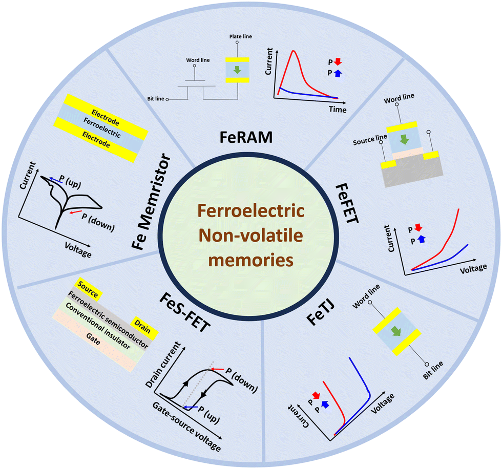 | ||
| Fig. 1 Different types of ferroelectric non-volatile memories that are applicable to neuromorphic computing and their corresponding current responses. | ||
2. Evolution of ferroelectric materials for non-volatile memory devices
In the electronics area, recent applications include ferroelectric non-volatile memory devices, which can be considered as the basic building blocks for neuromorphic computing devices.4,7,8 Ferroelectric materials possess the ability to switch, upon appropriate voltage application, the polarization direction of their remanent polarization (Pr), which is stable at zero electric field. This offers features like fast read/write speed, low power consumption, and high reliability compared with conventional floating-gate electrically erasable programmable read-only memory (EEPROM) and flash EEPROM devices, which require long read/write times and high voltages.8 Furthermore, ferroelectric materials can offer unique gradual domain switching characteristics, which provide the aforementioned multi-level conductance/resistance functionality. As a result, there is an increased interest in ferroelectric materials for non-volatile memory and neuromorphic applications. Fig. 2 shows the evolution of the number of publications per year since 1998, using the keywords ‘ferroelectric materials and memory applications’ in a Web of Science search. Up to 2013, the number of publications remained almost constant and then increased exponentially. This is linked to the discovery of new ferroelectric materials, as discussed below.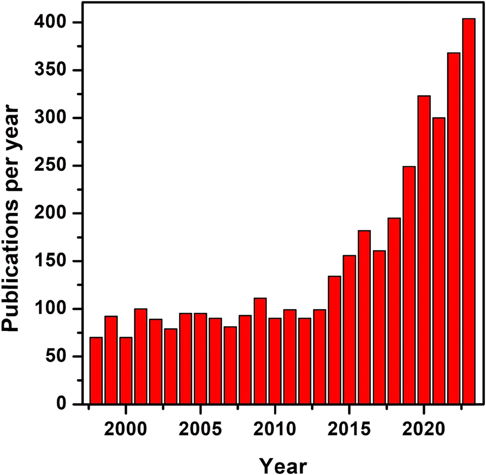 | ||
| Fig. 2 Publications per year based on ferroelectric memories from the year 1998 up to 2023 [Analyze Results (webofscience.com)]. | ||
Perovskite-based ferroelectric materials such as lead zirconate titanate (PZT) and strontium bismuth tantalate (SBT) are promising materials for achieving the performance required for memory applications such as logic-in memory (LiM) and non-volatile logic devices.9–17 For instance, different companies (such as Cypress Semiconductor, Texas Instruments, and Fujitsu) installed a PZT-based FeRAM in applications, including wearable medical gadgets, smart cards, energy meters, airplane black boxes, radio frequency tags, and code storage in microcontrollers.11 SBT-based FeFETs with a huge memory window and almost infinite cycling endurance (>1012) were demonstrated by Sakai et al.,12 which later exhibited adequate operation in non-volatile logic (NVL) circuits12 and 64 kbit NAND memory arrays.13 However, while recent investigations concentrated on the continued physical scaling-down of the metal–oxide–semiconductor field-effect transistor (MOSFET),13,15 the integration of perovskite oxides with front-end semiconductor manufacturing processes faced difficulties, particularly those related to perovskite etching, high crystallization temperature, hydrogen sensitivity, thickness, and cell size scaling beyond the 130 nm technology node.9,11 For instance, PZT experiences scalability problems,9,11 because it often loses its polarization in thin films at the nanoscale due to large depolarization fields. Increasingly, 3D integration is required for high-density memory technology with constantly decreasing dimensions, which exacerbates the scaling difficulties for perovskite ferroelectric films at the industrial level.11 Furthermore, PZT contains lead, which makes it toxic with serious health implications.
Considering the aforementioned challenges of perovskites, the discovery of ferroelectricity in Si-doped hafnium oxide (Si:HfO2) thin films has provided a promising alternative to resolve these problems.15,16 Following this exciting discovery, ferroelectricity in the nano-regime in Si:HfO2 has attracted significant attention from the ferroelectrics community due to its compatibility with the complementary metal–oxide–semiconductor (CMOS) technology. Inducing ferroelectricity at the nanoscale is the current trend in non-volatile memories to realize applications such as high-density memory, storage class memory, neuromorphic computing, hardware security, etc.17 Recent progress in this field has introduced new ferroelectric materials besides Si:HfO2 with promising ferroelectric polarization and superior scalability to the nanoscale regime that are compatible with CMOS for the next-generation ferroelectric memories as shown in Fig. 3.18–34Fig. 3 also provides some keywords for the enhancement of Pr with moderate coercive field (Ec) values (1–2 MV cm−1), which can induce large memory windows in non-volatile memory devices such as FeFETs for non-destructive readout operations.1 For FeFETs, however, a moderate Pr is already ideal, as too high of a Pr value can deteriorate the device reliability due to a high depolarization field and a high concentration of trapped charges.1Fig. 3 clearly provides a picture that orthorhombic (o-) Hf0.5Zr0.5O2 is at an advanced stage compared with other ferroelectric materials in terms of achieving good Pr, low Ec, and excellent CMOS compatibility. Table 1 complements Fig. 3, showing further details such as preparation methods, electrode materials, and film thicknesses, which were used in the ferroelectric-based devices, together with other relevant key ferroelectric performance indicators such as required wake-up cycles (the number of switching cycles required to achieve the maximum Pr), endurance, Curie temperature (Tc), etc. With this as the background, this short review focuses on the breakthroughs in the newly introduced ferroelectric materials from the viewpoint of their ferroelectric properties and how they are beneficial for neuromorphic applications. Finally, we conclude the review article with a perspective on this burgeoning area.
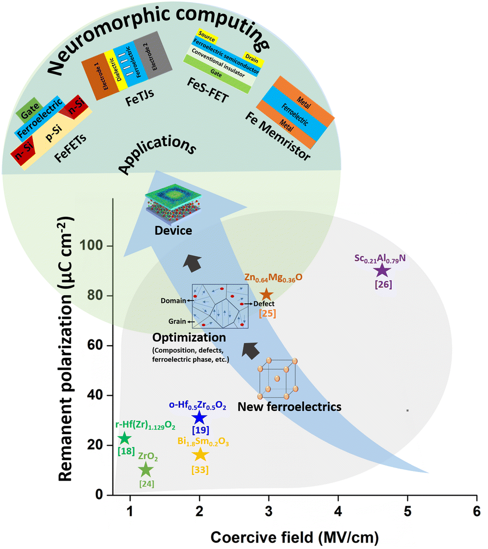 | ||
| Fig. 3 New ferroelectric materials and their possible applications. o- and r- indicate orthorhombic and rhombohedral phases, respectively. | ||
| Material and thickness | Method | P r (μC cm−2) | E c (MV cm−1) | T c (K) | Wake-up (cycle) | Endurance (cycles) | Top/bottom electrodes | Substrate | Ref. |
|---|---|---|---|---|---|---|---|---|---|
| *PLD – pulsed laser deposition, ALD – atomic layer deposition, IBSD – ion bean sputtering deposition, MBE – molecular beam epitaxy, PVD – physical vapor deposition, and CSM – chemical solution method | |||||||||
| Hf(Zr)1.129O2 (12 nm) | Sputtering | 22 | 0.65 | — | None | 1012 | TiN (top and bottom) | Si | 18 |
| Hf0.5Zr0.5O2 (20 nm) | ALD | ∼1.07 | ∼19 | — | Needed | 104 | Ni/Pt | SiO2/Si | 19 |
| Hf0.5Zr0.5O2 (10 nm) | ALD | ∼30 | ∼2 | — | None | 104 | W (top and bottom) | SiO2/Si | 19 |
| Hf0.5Zr0.5O2 (11 nm) | Sputtering | ∼1 | ∼10 | — | Needed | 104 | TiN/Pt | SiO2/Si | 20 |
| Hf0.5Zr0.5O2 (9 nm) | ALD | ∼1 | ∼21.7 | — | Needed | 105 | TiN/Pt | SiO2/Si | 21 |
| Hf0.5Zr0.5O2 (5 nm) | PLD | ∼5 | ∼34 | — | None | — | La0.7Sr0.3MnO3 (top and bottom) | SrTiO3 | 22 |
| ZrO2 (30 nm) | CVM | 8.5 | — | — | — | 103 | TiN/Pt | Si (100) | 23 |
| ZrO2 (8 nm) | IBSD | 9.3 | 1.2 | — | None | 106 | Au (top) | Nb:SrTiO3 | 24 |
| Zn0.64Mg0.36O (300 nm) | Sputtering | 80 | 3 | — | 20 | 103 | Pt (top and bottom) | SiO2/Si | 25 |
| Al0.79Sc0.21N (100 nm) | MBE | 90 | 4.6 | — | — | 105 | Au/n-type GaN | Si | 26 |
| Al0.7Sc0.30N (45 nm) | Sputtering | 100 | >5 | — | — | — | TiN (top and bottom) | SiO2/Si | 27 |
| Al0.64Sc0.36N (30 nm) | Sputtering | 100 | >6 | — | — | <105 | TiN (top and bottom) | SiO2/Si | 28 |
| Al0.64Sc0.36N (16 nm) | Sputtering | 30 | 6.5 | — | — | — | Pt (top and bottom) | SiO2/Si | 29 |
| Sc0.30Al0.7N (5 nm) | MBE | 23 | >6 | — | — | — | Mo (top and bottom) | Mo | 30 |
| Al0.72Sc0.28N (5 nm) | PVD | >100 | 9.2 | — | — | — | Al (top and bottom) | Sapphire | 31 |
| Al0.64Sc0.36N (100 nm) | Sputtering | 80 | 2 | — | — | 104 | Ti–Au/Pt | Si | 32 |
| Bi1.8Sm0.2O3 (1 nm) | Sol–gel | 17 | ∼2 | 473 | — | 108 | Au (top) | Nb:SrTiO3 | 33 |
| Bi1.8Sm0.2O3 (4.6 nm) | CSM | 50 | 0.75 | — | — | 109 | Au/Cr (top) | Nb:SrTiO3 | 34 |
3. Novel ferroelectric materials for neuromorphics
3.1 HfO2 and ZrO2-based films
Since the discovery of ferroelectricity in Si-doped hafnium oxide in 2011, doped hafnium oxide has been receiving significant attention.35 The discovery of CMOS-compatible and scalable ferroelectric materials has excited the ferroelectrics community.35,36 Following this, there have been extensive investigations into its fundamentals and applications. Hafnium oxide typically adopts a stable monoclinic phase (P21/c) at room temperature, a tetragonal (P42/mnc) structure at >2100 K, and a cubic (Fm![[3 with combining macron]](https://www.rsc.org/images/entities/char_0033_0304.gif) m) structure at >2800 K.35,36 These phases are non-polar, i.e., non-ferroelectric. So far, there have been a tremendous number of studies, experimental and computational, investigating the stabilization of meta-stable polar phases. Ferroelectricity in hafnium- and zirconium-based oxides arises from meta-stable, polar orthorhombic (o-) or rhombohedral (r-) phases with space groups Pca21 or R3m.22,37 In addition, several factors including doping, deposition method, post-deposition treatment, interface chemistry, etc. have shown to enhance the ferroelectric performance of these materials.38–40 In terms of doping, numerous dopants have been investigated such as Si, La, Gd, Y, Sr, Al, and Zr.38–47 Out of all the dopants in hafnium oxide, zirconium shows the most promise owing to the robust ferroelectric properties upon introducing it. Wei et al. reported wake-up-free ferroelectric switching in ultra-thin Hf0.5Zr0.5O2 films (thickness of 5 nm) by stabilizing the ferroelectric r-phase using a compressive epitaxial strain engineering strategy.22 Recently, the same group reported that the polarization switching in r-phase Hf0.5Zr0.5O2 films (thickness of 6 nm) might be ascribed to reversible oxygen vacancy migration.45 In another work, Stylianidis et al. reported ferroelectricity in 5-nm-thick Hf0.5Zr0.5O2 films also attributable to the polarization switching driven by oxygen vacancy migration.46 Yun et al., on the other hand, confirmed polarization switching in yttrium-doped HfO2 with an o-phase with a small rhombohedral distortion attributable to “true” ferroelectricity, i.e., the reversible switching of the material's unit cell polarization.47 The electrical switchability of the yttrium-doped HfO2 films studied using piezo-response force microscopy revealed features of “intrinsic” ferroelectricity not obscured by extrinsic factors like charge injection. Overall, the phenomenon of ferroelectric switching in hafnia-based films is still under debate regarding the origin of the observed polarization switching.45,46 The minimum film thickness that demonstrated ferroelectricity in Zr-doped HfO2 (Hf1−xZrxO2) with x = 0.2 was 1 nm, which was grown by low-temperature atomic layer deposition (ALD) on a silicon substrate, followed by rapid thermal annealing.48 Furthermore, the Zr-doped composition Hf1−xZrxO2, with x = 0.5, is the most promising one for its excellent ferroelectric properties attributable to the stable ferroelectric orthorhombic phase (Pbc21) due to the ferroelectric phase transition in the HfO2–ZrO2 solid solution.38
m) structure at >2800 K.35,36 These phases are non-polar, i.e., non-ferroelectric. So far, there have been a tremendous number of studies, experimental and computational, investigating the stabilization of meta-stable polar phases. Ferroelectricity in hafnium- and zirconium-based oxides arises from meta-stable, polar orthorhombic (o-) or rhombohedral (r-) phases with space groups Pca21 or R3m.22,37 In addition, several factors including doping, deposition method, post-deposition treatment, interface chemistry, etc. have shown to enhance the ferroelectric performance of these materials.38–40 In terms of doping, numerous dopants have been investigated such as Si, La, Gd, Y, Sr, Al, and Zr.38–47 Out of all the dopants in hafnium oxide, zirconium shows the most promise owing to the robust ferroelectric properties upon introducing it. Wei et al. reported wake-up-free ferroelectric switching in ultra-thin Hf0.5Zr0.5O2 films (thickness of 5 nm) by stabilizing the ferroelectric r-phase using a compressive epitaxial strain engineering strategy.22 Recently, the same group reported that the polarization switching in r-phase Hf0.5Zr0.5O2 films (thickness of 6 nm) might be ascribed to reversible oxygen vacancy migration.45 In another work, Stylianidis et al. reported ferroelectricity in 5-nm-thick Hf0.5Zr0.5O2 films also attributable to the polarization switching driven by oxygen vacancy migration.46 Yun et al., on the other hand, confirmed polarization switching in yttrium-doped HfO2 with an o-phase with a small rhombohedral distortion attributable to “true” ferroelectricity, i.e., the reversible switching of the material's unit cell polarization.47 The electrical switchability of the yttrium-doped HfO2 films studied using piezo-response force microscopy revealed features of “intrinsic” ferroelectricity not obscured by extrinsic factors like charge injection. Overall, the phenomenon of ferroelectric switching in hafnia-based films is still under debate regarding the origin of the observed polarization switching.45,46 The minimum film thickness that demonstrated ferroelectricity in Zr-doped HfO2 (Hf1−xZrxO2) with x = 0.2 was 1 nm, which was grown by low-temperature atomic layer deposition (ALD) on a silicon substrate, followed by rapid thermal annealing.48 Furthermore, the Zr-doped composition Hf1−xZrxO2, with x = 0.5, is the most promising one for its excellent ferroelectric properties attributable to the stable ferroelectric orthorhombic phase (Pbc21) due to the ferroelectric phase transition in the HfO2–ZrO2 solid solution.38
There have been many attempts to deposit ferroelectric Hf0.5Zr0.5O2 (HZO) using various deposition techniques such as ALD, pulsed laser deposition (PLD), metal–organic chemical vapor deposition (MOCVD), or sputtering.49–56 In the early stages of research, most HZO films were deposited using ALD on top of Si, SiO2 or TiN, followed by a rapid thermal annealing (RTA) step.39–41 Generally, an Ec value of ∼1 MV cm−1 and a remanent polarization Pr value of >15 μC cm−2 were achieved.45,47 ALD-grown HZO films tend to demonstrate wake-up behavior, which means that they require a number of applied voltage cycles prior to the actual demonstration of ferroelectric behavior or before reaching their maximum Pr value. There have been multiple attempts to mitigate this wake-up effect and some reports demonstrated wake-up-free ALD-grown HZO through capping electrode engineering, mechanical stress, and plasma treatment.10 Furthermore, epitaxial HZO has been investigated, mainly using PLD. While PLD is currently not CMOS-compatible like ALD, it enables understanding of fundamental properties about the origin of ferroelectricity in HZO with highly crystallized single-phase films. HZO films have been grown on SrTiO3 (STO) (001) with the La0.67Sr0.33MnO3 (LSMO) buffer layer55–58 and they typically demonstrate o-(111) oriented films. However, in 2018, Y. Wei et al. reported r-(111) ferroelectric films for the first time.28 The factors determining the formation of a specific ferroelectric phase remain unclear. Recent studies conducted by S. Estandia et al., 2021,57 and S. Shi et al., 2023,58 have highlighted the significant role of the bottom electrode in achieving the ferroelectric o-phase. Their findings indicate that MnO termination of LSMO is necessary for the formation of the o-phase. Epitaxial o-HZO films tend to have a high Ec of >3 MV cm−1 (depending on their thickness) and Pr > 30 μC cm−2. It is unclear at present which termination or other structural aspects of LSMO are needed to achieve the r-phase. In addition, recently, magnetron-sputtered r-Hf(Zr1.129)O2 films have shown a very good Pr of 22 μC cm−2, an ultra-low Ec of 0.65 MV cm−1, and stable performance up to ∼1012 cycles, which seem to solve the problem of high Ec in o-phase HfO2-based films. The demonstrated stabilization of the r-phase and its associated ferroelectric properties are attributed to intercalated atoms that expand the lattice, thereby increasing both in-plane and out-of-plane stresses, thus creating a more highly polarised structure, which is easier to switch due to its lower kinetic energy barrier between the two spontaneous polarization states.18
Rapid development of nanoscale HfO2-based materials with excellent ferroelectric properties and available multi-level conductance states, along with their physical dimensions and compatibility with CMOS technology, has inspired the adoption of these materials into synaptic devices with low footprints and high energy efficiency.49–56 The key parameters that determine the ideal requirement for a synaptic device are high Pr, moderate Ec, large on/off ratio, long cycling endurance, prolonged retention, and well-spaced conductance levels.4 For instance, ferroelectric materials can achieve multi-level Pr states by varying the applied electric switching field. Not only that, these materials maintain each state even after removal of the electric field. This multi-level Pr can be used to modulate the conductance of the synaptic device.59,60 The low Ec can extend the endurance lifetime and result in low-voltage switching for non-volatile memories.61 A large on/off ratio potentially increases the number of multi-level states by providing a large memory window.4,62 Moreover, the endurance and retention of the ferroelectric materials allow the memory device to store the data over a long time.62 Therefore, we can say that ferroelectric-based non-volatile memory devices are promising for synaptic elements in neuromorphic computing.
Recently, researchers have reported analog synaptic transistors based on HfO2- and ZrO2-based ferroelectric materials, which employ a variety of channel materials, including WOx, indium gallium zinc oxide (IGZO), indium zinc tin oxide (IZTO), poly-GeSn, and WS2.63–69 HfO2- and ZrO2-based ferroelectric materials are attractive due to their ferroelectricity in ultra-thin films (from ∼1 up to 10 nm) with improved reliability, low programming voltage and CMOS compatibility.63–66 For instance, Halter et al. studied an Hf0.57Zr0.43O2 thin-film-based (thickness ∼9.6 nm) FeFET with WOx as the channel material for synaptic elements.63 This work showcased an Hf0.57Zr0.43O2/WOx stack as an FeFET with good voltage control and strong linearity and symmetry in potentiation and depression at different voltage amplitudes with identical pulse trains, which facilitate facile programming of learning algorithms. The FeFET has a short programming time of 40 ns and a low write energy (2.1 × 10⁻¹⁷ J μm−2). Furthermore, it offers multi-level programming spanning more than 4 bit depth and a stable retention over 1500 s. Moreover, the device is compatible with a back end of line (BEOL) integration into standard CMOS processes. Kim et al. reported Al-doped HfO2 with improved switching speed (∼107 mV per decade) and a good on/off ratio (1 × 10³), demonstrating its use as a potential synaptic transistor.65 By varying the amplitude and number of input pulses, this work was able to achieve potentiation/depression weight updates with minimal cycle-to-cycle variability and good linearity. With the performance data of this FeFET, a simulated pattern recognition accuracy of almost 90% was achieved for the Modified National Institute of Standard and Technology (MNIST) handwritten data set under optimal potentiation/depression conditions. Furthermore, Al-doped HfO2 suppresses electrically active charge traps typically arising from the direct deposition of HfO2 on Si and favors analog conduction modulation at low operating voltages.
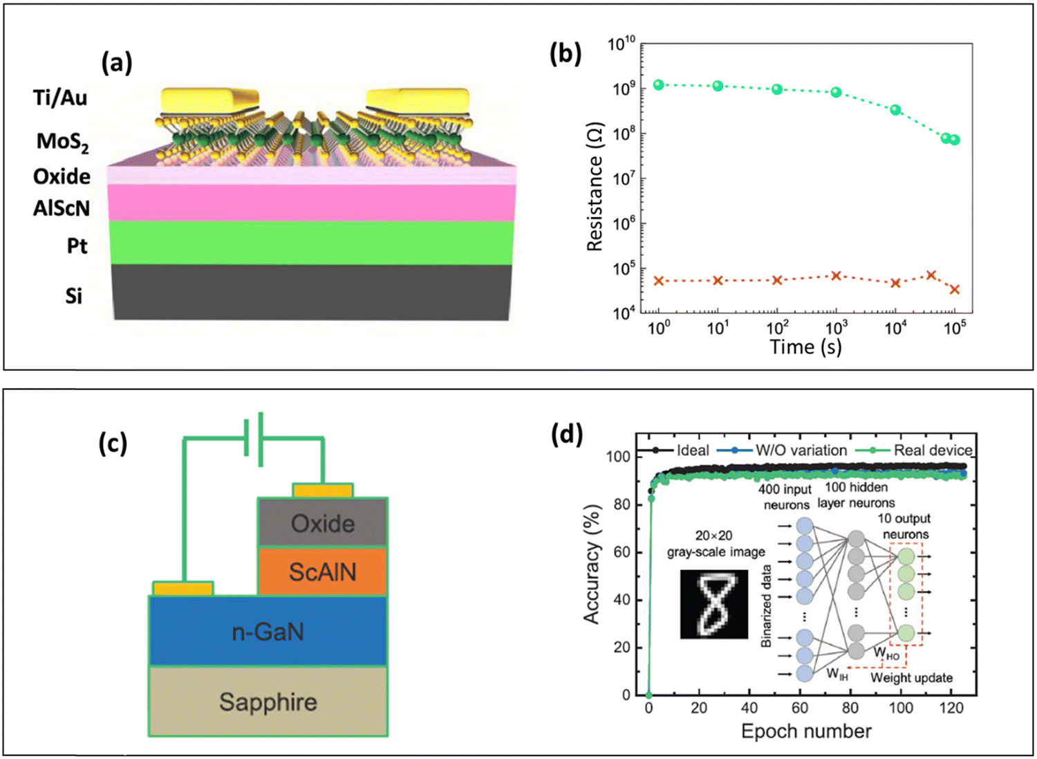
Bégon-Lours et al. developed a 3.5-nm-thick Hf0.5Zr0.5O2 thin film transistor with an on/off ratio of 7 and a small device-to-device variability (<5%) suitable for neural network inference.67 Furthermore, the device operates in the ohmic regime for the read-out, which is good for analog vector-matrix multiplication. The conduction modulation in the transistor may have originated from the motion of trapped hydrogen in the lattice and/or oxygen vacancies that form during ALD fabrication. These defects modify the conduction band energy profile and transport properties upon polarization switching. As a synaptic element, this transistor demonstrated a training accuracy of 92% after 36 epochs on the MNIST data set. Xi et al. experimentally demonstrated a CMOS-compatible FeFET using an Hf0.5Zr0.5O2 ferroelectric layer (thickness ∼10 nm, Fig. 4(a)) with a very high on/off ratio (3 × 10⁴) and low write energy consumption (∼2 fJ) at low voltages (0.5 V) (Fig. 4(b)).68 This synaptic device was based on Hf0.5Zr0.5O2/NiSi2/Si and used partial polarization switching to modulate the Schottky barrier of the NiSi2/Si contacts for analog conduction modulation with symmetric potentiation/depression characteristics and high retention.
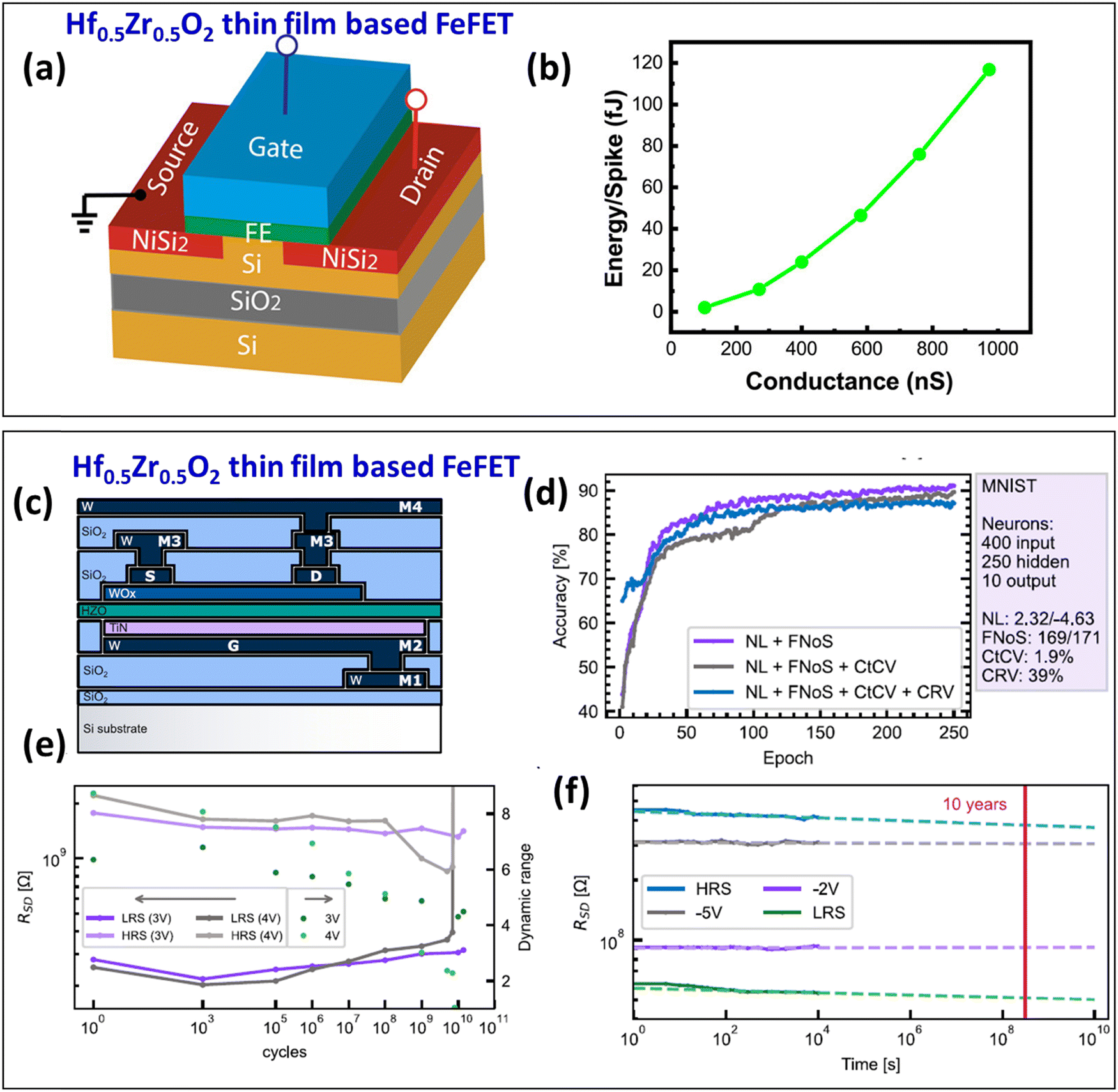 | ||
| Fig. 4 (a) Schematic diagram of an Hf0.5Zr0.5O2 thin-film-based 3-terminal FeFET. (b) Calculated energy/spike consumption at different voltage pulse amplitudes.68 Copyright (2020) by American Chemical Society. (c) Illustration of an FeFET device based on an Hf0.5Zr0.5O2 thin film with source (S), drain (D), gate (G), WOx channels, ferroelectric gate dielectric, access metal lines (M1, M2), plus S access metal line (M3) and D access metal line (M4). (d) MNIST classification performance of the FeFET with different degrees of non-idealities included: non-linearity factors and finite number of steps (purple), added cycle to cycle variation (grey), and added conductance range variation (blue). (e) Endurance measurement of the FeFET at 100 kHz. (f) Retention measurements at room temperature for the four programmed states69 with extrapolation to 10 years. | ||
Very recently, Halter et al. reported an Hf0.5Zr0.5O2 thin film FeFET (thickness ∼10 nm) (Fig. 4(c)) with good Pr (∼14 μC cm−2) and a very low write energy (1.2 fJ) at higher voltages (6 V).69 In terms of neuromorphic behavior, using the NeuroSim framework, a good MNIST classification accuracy of 88% was achieved (Fig. 4(d)) due to fine-grained, quasi-continuous monotonic resistance changes with more than 200 steps between the low and high resistance states and a low cycle-to-cycle variability. Furthermore, a very minimal dynamic range loss with a very high endurance (>1010 cycles) and an outstanding retention (>10 years) was achieved (Fig. 4(e) and (f)). As a result, the FeFET is promising for neural network inference and cognitive computing.
In a different study, Mikheev et al. fabricated a p-type Si/Hf0.5Zr0.5O2/TiN-based second-order memristor using a 4-nm-thin ferroelectric Hf0.5Zr0.5O2 ultra-thin film to investigate the synaptic functions for neuromorphic computing.70 In first-order memristors, the conductance is defined entirely by external stimuli and thus to emulate the temporal synapse response, an accurate overlapping of pre- and post-synaptic spikes is needed, which is not the case in biological synapses. In second-order memristors, the conductance is controlled by both the external stimuli and their instant internal state. These second-order memristors do not require particular spike shapes and their overlapping and thus allow a straightforward natural emulation of the frequency response. Mikheev et al. demonstrated conductivity (synaptic weight) modulation with ROFF/RON ∼ 8 via the gradual switching of polarization in ferroelectric domains of polycrystalline 4-nm-thin ferroelectric Hf0.5Zr0.5O2 films. The built-in electric field and charge trapping/de-trapping at the defect states at the Si interface contribute further to the temporal behavior, expressing modulation similar to synapses in biological systems. The work of Mikheev et al. also experimentally demonstrated synaptic functions such as short-term plasticity, paired-pulse facilitation (PPF), paired-pulse depression (PPD), and spike-rate-dependent plasticity (SRDP), which are similar to biological synaptic systems. Müller et al. developed another promising approach using an Fe memristor for the prospects of neuromorphic applications. A simple metal–ferroelectric–metal (MFM) structure utilizing an ultra-thin Hf0.93Y0.07O2 film of thickness 4.5 nm displayed a very good on/off ratio (540) and a large range of accessible resistance states for future NVM.66 This work introduces polarization-modulated charge transport from Schottky-barrier-limited to Ohmic conduction, reporting a high on/off ratio for ultrathin epitaxial Hf0.93Y0.07O2 films. The impact of the polarization reversal on the charge transport across a MFM device, utilizing a partially depleted insulating ferroelectric barrier, is demonstrated, which is conceptually different from those in FeTJs, where a fully depleted insulating ferroelectric barrier is used.
From these examples, it can be concluded that these HfO2- and ZrO2-based materials are all viable options for large-scale integration into neuromorphic hardware. However, one of the critical outstanding challenges with HfO2 and ZrO2 FeFETs are wake-up effects, about which no information has been provided in any of the reviewed examples.
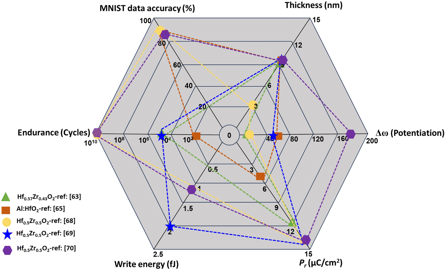
Table 2 shows some key reports on HfO2- and ZrO2-based synaptic transistors, including features like Pr, endurance pulse information, write pulse duration, on/off ratio, synaptic weight, and write energy. Fig. 5 complements Table 2 in terms of the key parameters (thickness, Pr, endurance, the number of conductance levels ω, and write energy) of HfO2- and ZrO2-based materials for application as synaptic devices. It can be concluded that reducing the thickness of the ferroelectric layer below 10 nm causes degradation of the potentiation/depression due to increased leakage currents during the program/erase process.4 Unfortunately, there is not much information available about the write energy and MNIST data accuracy except for Hf0.5Zr0.5O2 thin film FeFETs, which are considered to be key neuromorphic parameters. FeS-FET device structures are not currently being investigated on a large scale, while FeTJs and Fe memristors have been scarcely investigated.
| Device structure | P r (μC cm−2) | Endurance (cycles) | Voltage range for potentiation & depression | Write pulse duration (μs) | On/off ratio | Conductance levels Δω for potentiation/depression | Write energy (fJ) | Ref. |
|---|---|---|---|---|---|---|---|---|
| Al2O3/WOx/Hf0.57Zr0.43O2 (9.6 nm)/TiN/Si (FeFET) | ∼12 | 105 | 1 to 3.1 V and −0.9 to −3 V (incremental) | 10 | 1.9 | 22/22 | — | 63 |
| ITO/IGZO/Al:HfO2 (10 nm)/W/p-Si(FeFET) | ∼5 | 102 | 1.9 to 4 V and −1.2 to −3.3 V (incremental) | 1 | 1 × 10³ | 70/70 | — | 65 |
| W/Hf0.57Zr0.5O2 (5 nm)/n-SrTiO3/Si(FeTJ) | ∼14 | — | −2 V and 2 V (identical) | 50 | 1.55 | 16/16 | 8 | 64 |
| TiN/Hf0.5Zr0.5O2 (3.5 nm)/WOx/SiO2/Si(FeFET) | ∼14 | 1010 | −1.4 V and 2 V (unidentical) | 0.02 | 7 | 25/25 | — | 67 |
| TiN/Hf0.5Zr0.5O2(10 nm)/TiN/SiO2/Si (FeFET) | ∼14 | 105 | 0.5 V and −0.5 V (identical) | 1 | 3 × 10⁴ | 50/50 | 2 | 68 |
| TiN/Hf0.5Zr0.5O2 (10 nm)/WOx/SiO2/Si (FeFET) | ∼14 | 1010 | 0.6 V to 5 V and −1.25 V to −5.5 V (incremental) | 500 | — | 171/169 | 1.2 | 69 |
| Au/Hf0.93Y0.07O2 (4.5 nm)/La0.7Sr0.3MnO3/Nb–SrTiO3 (Fe Memristor) | — | 1.5 to 4 V and −1.5 to −4 V (incremental) | 10![[thin space (1/6-em)]](https://www.rsc.org/images/entities/char_2009.gif) 000 000 |
540 | 50/50 | — | 66 |
 | ||
| Fig. 5 Performance of HfO2- and ZrO2-based FeFETs for different key parameters that are required for neuromorphic computing devices. | ||
Just as with HfO2, pure or doped ZrO2-based thin films are promising for high-k gate dielectrics and are compatible with CMOS technology, and it is surprising that the material has been seldom investigated for ferroelectricity.71–74 In 2016, Fan et al. fabricated ZrO2 films using magnetron sputtering and stabilized the ferroelectric o-phase by substrate-induced strain to form highly textured (111) ZrO2 ferroelectric films.72 It was found that the o-phase is stabilized by applying compressive strain along the in-plane 〈11![[2 with combining macron]](https://www.rsc.org/images/entities/char_0032_0304.gif) 〉 direction. Consequently, a phase transition from the tetragonal (t-) phase to the ferroelectric o-phase occurred in the ZrO2 film. Lin et al. verified the existence of a ferroelectric o-phase in undoped ZrO2 films (10 nm thick) made by remote plasma ALD.73 More recently, Wang et al. reported a Pr of 8.5 μC cm−2 and a high relative permittivity of 39.6 in 30-nm-thick pure ZrO2 films grown on Si (100) via chemical solution deposition.23 Ferroelectricity in pure ZrO2 films is established after a wake-up operation of about 1000 cycles. According to Wang et al., the wake-up process induces ferroelectricity by changing the non-ferroelectric t-phase to a ferroelectric o-phase via oxygen loss. In addition, it was found that an increase in film thickness (40 nm and 50 nm) weakened the ferroelectric behavior and this was ascribed to the phase transformation from the o-phase to the cubic phase as strain relaxes with thickness. In the same year, Silva et al. showed ferroelectricity in r-phase ZrO2 thin films without any wake-up process.20 The films were grown on (111)-oriented Nb:SrTiO3 (Nb:STO) using ion beam sputtering. Ferroelectricity in these ZrO2 thin films is attributed to the formation of a polar r-(R3m) phase under epitaxial compressive strain. Pole figure measurements of the 8-nm-thick ZrO2 thin films confirmed the plane distances d200= d020= d002 in the range between 2.55 Å and 2.50 Å, indicative of an r-space group. The films displayed a spontaneous polarization Ps of 20 μC cm−2 and a Pr of 10.8 μC cm−2 with an Ec of 1.5 MV cm−1. By converting an anti-ferroelectric t-phase to a ferroelectric o-phase, Cheema et al. introduced a strategy to achieve ferroelectricity in ZrO2 films through reduced dimensionality.71 The films were deposited using ALD. This work reduced the ZrO2 film thickness down to 5 Å and stabilized the ferroelectric o-phase. The reduced dimensionality can be achieved through hydrostatic pressure, chemical pressure, or epitaxial strain.71 Very recently, Silva et al. stabilized the o-phase in 8-nm-thick ZrO2 films deposited using ion beam sputtering on Nb:STO substrate.20 The films displayed a Pr of 9.3 μC cm−2 and an Ec of 1.2 MV cm−1 without any wake-up process. The lack of wake-up effect is attractive for next-generation memory devices. However, the potential application of ferroelectric ZrO2 in neuromorphics is yet to be demonstrated.
〉 direction. Consequently, a phase transition from the tetragonal (t-) phase to the ferroelectric o-phase occurred in the ZrO2 film. Lin et al. verified the existence of a ferroelectric o-phase in undoped ZrO2 films (10 nm thick) made by remote plasma ALD.73 More recently, Wang et al. reported a Pr of 8.5 μC cm−2 and a high relative permittivity of 39.6 in 30-nm-thick pure ZrO2 films grown on Si (100) via chemical solution deposition.23 Ferroelectricity in pure ZrO2 films is established after a wake-up operation of about 1000 cycles. According to Wang et al., the wake-up process induces ferroelectricity by changing the non-ferroelectric t-phase to a ferroelectric o-phase via oxygen loss. In addition, it was found that an increase in film thickness (40 nm and 50 nm) weakened the ferroelectric behavior and this was ascribed to the phase transformation from the o-phase to the cubic phase as strain relaxes with thickness. In the same year, Silva et al. showed ferroelectricity in r-phase ZrO2 thin films without any wake-up process.20 The films were grown on (111)-oriented Nb:SrTiO3 (Nb:STO) using ion beam sputtering. Ferroelectricity in these ZrO2 thin films is attributed to the formation of a polar r-(R3m) phase under epitaxial compressive strain. Pole figure measurements of the 8-nm-thick ZrO2 thin films confirmed the plane distances d200= d020= d002 in the range between 2.55 Å and 2.50 Å, indicative of an r-space group. The films displayed a spontaneous polarization Ps of 20 μC cm−2 and a Pr of 10.8 μC cm−2 with an Ec of 1.5 MV cm−1. By converting an anti-ferroelectric t-phase to a ferroelectric o-phase, Cheema et al. introduced a strategy to achieve ferroelectricity in ZrO2 films through reduced dimensionality.71 The films were deposited using ALD. This work reduced the ZrO2 film thickness down to 5 Å and stabilized the ferroelectric o-phase. The reduced dimensionality can be achieved through hydrostatic pressure, chemical pressure, or epitaxial strain.71 Very recently, Silva et al. stabilized the o-phase in 8-nm-thick ZrO2 films deposited using ion beam sputtering on Nb:STO substrate.20 The films displayed a Pr of 9.3 μC cm−2 and an Ec of 1.2 MV cm−1 without any wake-up process. The lack of wake-up effect is attractive for next-generation memory devices. However, the potential application of ferroelectric ZrO2 in neuromorphics is yet to be demonstrated.
3.2 Doped zinc oxide films
ZnO is regarded as a conventional non-ferroelectric II–VI wurtzite semiconductor material with a band gap ∼3.4 eV.75 Theoretical investigations done by Moriwake et al., however, reported the possibility of a spontaneous polarization Ps of ∼ 90 μC cm−2 in wurtzite ZnO due to the structural distortion arising from the relative displacement of cations against anions along the c-axis.75,76 This is attributed to the tensile strain experienced along the ab-plane along the [0001] direction. Consequently, the potential barrier obstructing the polarization rotation is reduced and the non-polar P63/mmc switches between two equivalent polar states (P63mc), inducing ferroelectricity.76In order to make ZnO attractive as a ferroelectric tunneling resistive memory for low power non-volatile memory devices with fast switching speeds, appropriate dopants such as Li, Mn, Co, Cr, and Ti are required both to tune the band gap of ZnO and to enhance its ferroelectricity.77–79 Onodera et al. reported ferroelectric behavior in wurtzite-structured Li-doped ZnO bulk ceramics with a modest Pr of ∼ 0.044 μC cm−2 at ambient temperature using P–E hysteresis loop measurements. Here, the Li ion occupies the off-centered positions, replacing Zn ions. This forms electric dipoles to induce ferroelectric polarization.79 Yang et al. reported ferroelectric polarization in V-doped ZnO thin films deposited on Si(111) substrates with a Pr of ∼0.2 μC cm−2 using magnetron co-sputtering. The introduction of V5+ at Zn2+ sites affects the 3d–2p hybridization and induces a local dipole moment by changing the Zn(V)–O bond length.77 While the principal demonstration of ferroelectricity in ZnO is promising, the low Pr in these doped ZnO films obviously requires improvement, possibly by optimizing the dopant type and concentration and strain levels.76–80
Recently, Mg has emerged as an ideal stressor not only capable of inducing superior ferroelectric properties, but also capable of stabilizing the wurtzite structure of ZnO.81–83 Jacques et al. reported a high Pr of ∼80 μC cm−2 and an Ec of ∼3 MV cm−1 for epitaxial Zn0.64Mg0.36O (ZMO) films (thickness ∼300 nm) deposited using magnetron sputtering with pure Zn and Mg targets.81 To induce ferroelectric switching, an applied electric field greater than Ec had to be applied for a sufficiently long duration to wake up the polarization states. The full realization of the ferroelectric switching in ZMO films was observed after 100 cycles with the application of an electric field of ∼5 MV cm−1. The excess electric field of 5 MV cm−1 had to be applied to overcome the internal electric field in the ZMO films due to increased deep trap states attributed to the migration of defects at the interfaces.81 In Zn1−xMgxO (ZnMgO) films of ∼500 nm thickness grown on single-crystal Al2O3, with x between 0.35 and 0.37, Ferri et al. reported ferroelectric switching with a Pr exceeding 100 μC cm−2 and an Ec less than 3 MV cm−1.82 The pronounced wake-up process in the ferroelectric ZnMgO films concluded after 100 cycles with an applied electric field greater than Ec. Ferri et al. also demonstrated the direct integration of ZnMgO films on flexible substrates such as kapton and polystyrene. This introduces the possibility of exploring, for the first time, ferroelectric switching in wurtzite solid solutions for neuromorphic computing. Despite the promising Pr values, however, a considerable decrease of Ec is needed to make ZnO realistic for neuromorphic applications. To achieve this, we anticipate that different strategies such as epitaxial growth, doping, strain engineering, domain engineering, etc. can be used.
3.3 Scandium-doped aluminum nitride (Al1−xScxN) films
Pure aluminum nitride (AlN) with a wurtzite structure is generally a pyroelectric material as its polarization direction cannot be switched with an applied electric field.69 According to the literature, however, ferroelectricity in AlN can be induced by adding Sc to it. This is ascribed to the elongation of the Al–N bond parallel to the c-axis, which arises due to the formation of a metastable hexagonal phase introduced by Sc.84–88 The layered hexagonal phase, particularly around the Sc site, is non-polar. The increase in the Sc content flattens the ionic potential towards the hexagonal phase and therefore reduces the energy barrier, which obstructs the polarization switching in the wurtzite structure of AlN.84–88 As a result, Sc-doped AlN experiences ferroelectric switching.Fichtner et al. reported a high Pr of ∼100 μC cm−2 with an Ec of ∼3 MV cm−1 in reactively sputtered Al0.64Sc0.36N films of thickness 400 nm deposited on oxidized Si(100) wafers.84 This excellent ferroelectricity in Al0.64Sc0.36N is associated with the existence of the hexagonal phase and compositional homogeneity, which allows only 180° orientation of domains. Besides, the Al0.64Sc0.36N film exhibits a piezoelectric coefficient of 15.7 pm V−1 with an excellent symmetry around the field axis. It should be noted that the increased Sc content above a particular limit causes a linear decrease in Ec. This was concluded from the composition analysis performed by Fichtner et al., where exceeding a certain threshold of Sc content impeded the ferroelectric properties again, favoring the formation of more of a non-polar layered hexagonal phase, which in turn distorts the wurtzite structure due to the expansion of the basal plane and the increasing length of the metal–nitrogen bond.84 Wang et al. fabricated Al0.71Sc0.29N thin film capacitors to demonstrate ferroelectric switching.89 The 100 nm Al0.71Sc0.29N thin film was deposited on Pt-coated Ti using magnetron sputtering. A wake-up operation up to 50 cycles was required to grow and stabilize the ferroelectric domains in the Al0.71Sc0.29N thin film. The Al0.71Sc0.29N thin film displayed a Pr of ∼100 μC cm−2 with an Ec of ∼5.5 MV cm−1 near room temperature. Further work performed by Wang et al. reported a record high Pr of ∼140 μC cm−2 and an Ec of ∼6.5 MV cm−1 in 20-nm-thick Al0.68Sc0.32N thin films near room temperature.90 The film was deposited on a Pt (111)/Ti/SiO2/Si wafer using magnetron sputtering. The formation of a strongly c-axis-oriented Al0.68Sc0.32N film was elucidated using X-ray diffraction and rocking curve measurements, which confirmed its highly crystalline nature with a full width at half maximum of 2.7°. The excellent ferroelectric switching in this Al0.68Sc0.32N film might be due to a combination of high crystalline nature, low film thickness, and a lower depolarization field at the surface oxide. Yasuoka et al. studied the effect of deposition conditions on Al1−xScxN thin films deposited on Pt(111)/Ti/SiO2/Si substrates using magnetron sputtering.91 The group investigated the effect of sputtering gas, film composition, and film thickness on the ferroelectric behavior of Al1−xScxN films. The Al1−xScxN films deposited under an N2 atmosphere showed good ferroelectricity compared with an N2 + Ar atmosphere. The smaller value of Pr in the Al1−xScxN film deposited under an N2 + Ar atmosphere might be attributed to the increased pinning of polarization states. The composition analysis of Al1−xScxN films in the range 0 < x < 0.34 displayed an increase in lattice parameter c up to 0.22 Å and showed a decreasing trend above this value. This indicates that the ferroelectricity is optimum for the composition x = 0.22 and is ascribed to the presence of more non-polar layered hexagonal phases for larger values of x, which contribute to the lengthening of the metal–nitrogen bond. Furthermore, the crystal structure analysis of the various thicknesses (48–140 nm) of Al1−xScxN films with x = 0.22 using rocking curve XRD analysis revealed that the preferential (002) orientation becomes predominant above 50 nm. Thus, the maximum values of Pr and the dielectric constant were found to be 129 μC cm−2 and 15.9, respectively, for the Al1−xScxN films with x = 0.22 and 140 nm thickness.91 Ryoo et al. reported a high Pr of ∼100 μC cm−2 and an Ec of >5 MV cm−1 in 45-nm-thick Al0.7Sc0.3N films deposited on a SiO2/Si substrate via sputtering.27 The enhanced ferroelectricity in the Al0.7Sc0.3N thin films arises from the imposed compressive strain, which eventually increases the c/a-lattice parameter ratio attributable to the enhanced (002)-preferred orientation. In another work, Kim et al. fabricated 30-nm-thick Al0.70Sc0.30N wurtzite thin films with a high Pr of 100 μC cm−2 with an Ec of >6 MV cm−1via sputtering deposition on a SiO2/Si substrate. This is ascribed to the highly c-axis-oriented crystal structure of the film favouring very good switching speed, eliminating the slow motion of the domain wall. Furthermore, a fatigue-free behavior (<105 cycles) was observed in the film.28 Musavigharavi et al. grew 20-nm-thick ferroelectric Al0.64Sc0.36N on a SiO2/Si substrate by sputtering. The work reported a maximum Pr of 30 μC cm−2 with an Ec of 6.5 MV cm−1. The large polarization is attributed to the formation of a highly crystalline wurtzite structure of Al0.64Sc0.36N at lower thickness with a preferential (002) orientation achieved normal to the SiO2/Si substrate.29 Wang et al., in 2023, reported ferroelectricity in ultra-thin Al0.7Sc0.3N deposited on a molybdenum (Mo) substrate using molecular beam epitaxy (MBE). The work displayed a Pr of 23 μC cm−2 with an Ec of > 6 MV cm−1.30 The group investigated the ferroelectric behavior of Al0.7Sc0.3N by varying the thickness from 100 to 5 nm. It is observed that the thickness decrease had a significant effect on Pr (decreases) and Ec (increases). The diminution in the ferroelectric polarization in the wurtzite Al0.7Sc0.3N ultra-thin films results from the high compressive strain induced by the scaling-down of the film thickness. Furthermore, in addition to the Janovec–Kay–Dunn (JKD) model (where Ec is proportional to d−2/3 with the film thickness d), the formation of a non-switchable “dead” layer or dielectric interfacial layer, or a finite screening length of the electrodes, contributes to the increase in Ec with the scaling down of the thickness. Zheng et al. developed ultra-thin Al0.72Sc0.28N films (thickness ∼5 nm) deposited on a sapphire substrate using physical vapor deposition and investigated their ferroelectric properties. The work showed Pr > 100 μC cm−2 with Ec ∼9.2 MV cm−1.31 This work suggests that the high Ec value for lower thickness may be due to the decrease in the c/a ratio arising from the Sc alloying ratio or from the film stress. Liu et al. fabricated an FeFET device, as shown in Fig. 6(a), composed of 100-nm-thick sputtered Al0.71Sc0.29N integrated with a two-dimensional (2D) molybdenum disulfide (MoS2) channel.32 The device achieved a high Pr of 80 μC cm−2 and an Ec of 6 MV cm−1. Furthermore, the device exhibited an excellent on/off ratio of ∼106, an endurance of 104 cycles, and a good retention of 105 s, which was however measured at a gate voltage of ±40 V, which is a very high writing voltage (Fig. 6(b)). The 2D MoS2 channel minimizes the depolarization field by compensating the incomplete charge induced by the ferroelectric Al0.71Sc0.29N layer, consequently providing prolonged retention and minimal read-disturb. Very recently, Wang et al. studied the ferroelectric and analog resistive switching of memristors in 5 nm wurtzite Al0.7Sc0.3N with gallium nitride (GaN) as the semiconductor channel grown on a sapphire substrate using MBE, as shown in Fig. 6(c).92 The device demonstrated its potential as a candidate for nonlinear ferroelectric resistive memory arrays with a high on/off ratio of 105, an endurance of >104 cycles, and a good retention of 105 s. Furthermore, the work displayed eight conductance states during potentiation and depression for the incremental pulse scheme with voltages ranging from −7.6 V to −8.24 V and 1.9 V to 3.564 V, respectively. However, some reports suggest that a minimum of ten conductance states during potentiation/depression are required for the effective training process by an ANN in the analog domain.92 Nevertheless, the device yielded a recognition accuracy of 92.9% from MNIST simulation (Fig. 6(d)).
 | ||
| Fig. 6 (a) Schematic diagram of a 100-nm-thick ferroelectric AlScN–MoS2 FeFET and (b) retention measurements made by monitoring the drain current at various time intervals of up to 100 000 s with a gate voltage of ±40 V. Copyright (2020) by American Chemical Society.32 (c) Illustration of an Fe memristor device using an AlScN ultra-thin film. (d) MNIST simulated classification performance of the AlScN Fe memristor showing the best recognition accuracy of 92.9% with non-linearity and cycle-to-cycle/device-to-device variations.92 | ||
Based on these promising demonstrations, we foresee that more studies on these high-Pr Al1−xScxN films could produce further synaptic elements with multi-level polarization states essential for analog conduction modulation during potentiation/depression with CMOS compatibility. Strategies like domain and strain engineering, as well as thickness reduction, could potentially be explored for reducing Ec to enhance the potential neuromorphic applicability.
3.4 Layered bismuth oxide films
Bismuth oxide is a classical ferroelectric material with a very high Curie temperature (∼673 K) and excellent cycling endurance (∼1012 cycles).93,94 This discovery builds on the finding of in-plane ferroelectricity in BiO layers in complex layered bismuth oxide compositions, e.g., Bi2AlMnO6 and Bi2NiMnO6. In these materials, the growth of the layered structure occurs more in the horizontal than in the vertical direction. It is reported that out-of-plane ferroelectric properties offer higher polarization switching than the in-plane orientation due to more uniform grains and ordered domains.95–98 Very recently, Yang et al. reported strong out-of-plane ferroelectricity in 1-nm-thin Sm-substituted bismuth oxide (Bi1.8Sm0.2O3) grown on an Al2O3 substrate using sol–gel spin-coating.99 The 1-nm-thin Bi1.8Sm0.2O3 (BSO) film exhibited a Pr of 17 μC cm−2, which is high compared with other ultra-thin films such as HZO, CuInP2S6, BaTiO3, BiFeO3, and PbZr0.2Ti0.8O3. Here, the Bi layers at the interface serve as strain bearers to relax the lattice mismatch from the substrate, thus maintaining an unstrained growth of the film. Even though the reduced thickness affects the ferroelectricity in the BSO film due to surface charges and leakage, the remarkable Pr arises due to the incorporation of the Sm dopants, which preserves the ferroelectric phase in the BSO and maintains a high polarization by suppressing the depolarization field. Furthermore, Sm promotes the tolerance of the layered Bi structure to uphold the stability of the ferroelectric structure at low dimensions. A slightly thicker film of 4.56-nm-thin BSO displayed a high Pr of 50 μC cm−2 with an Ec of about 0.75 MV cm−1. In addition, the film exhibited an excellent cycling endurance (∼108 cycles) and outstanding thermal stability (up to 493 K). The demonstrated Ec and Pr values at highly scaled film thicknesses are promising for neuromorphic applications such as non-destructive read/write operations and synaptic functionality. Hence, this new material warrants further deeper explorative studies of its neuromorphic behavior.Very recently, Gia et al. demonstrated an FeTJ based on an ultra-thin BSO film of thickness 4.6 nm deposited on Nb:STO using a chemical solution method (Fig. 7(a)).34 The FeTJ exhibited long retention time (10 years, Fig. 7(b)) and exceptional cycling endurance (109). The stable tetragonal-like phase induced by Sm substitution provided prolonged retention in the BSO-based FeTJs by reducing the depolarization field. Furthermore, the BSO film showed an excellent Pr of 50 μC cm−2 and a very low Ec of 0.75 MV cm−1. Moreover, the FeTJ displayed a large tunnelling electroresistance compared to other materials attributable to the large polarization maintained at the minute thickness (Fig. 7(c)). Consequently, both the ferroelectric barrier height and barrier width at the depletion region surface of Nb:STO were modulated. In this work, a single BSO-based FeTJ demonstrated 32 conductance states without any write-termination process. Hence, this new material warrants further deeper explorative studies of its neuromorphic behavior.
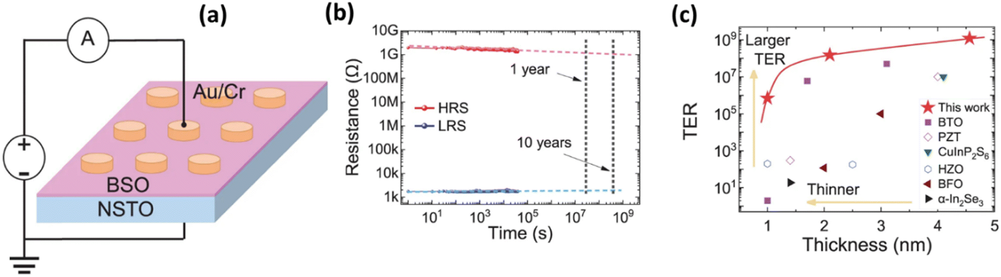 | ||
| Fig. 7 (a) Schematic diagram of a 4.6-nm-thin ferroelectric Bi1.8Sm0.2O3 (BSO) FeTJ device structure and (b) retention measurement indicating prolonged retention for more than 10 years by extrapolation. (c) Comparison of tunnelling electroresistance (TER) values of the BSO FTJ device with other ferroelectric materials and thicknesses.34 | ||
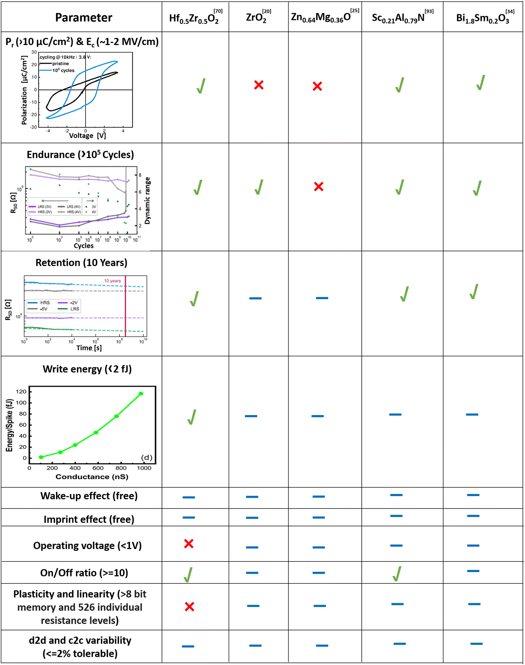
A summary comparing Pr, Ec, endurance, retention, and write energy of the different materials, together with neuromorphic performance parameters, is shown in Table 3. It is possible to conclude that Hf0.5Zr0.5O2 partially meets the requirements of neuromorphic applications. In the case of Hf0.5Zr0.5O2, we took the best performance56 from Fig. 5 to compare the neuromorphic parameters with other materials. However, these novel ferroelectrics are in the early stage of development and strong performance improvements are eagerly anticipated.
|
4. Concluding remarks
The recent discoveries of ferroelectricity in binary and pseudo-binary nanoscale oxide thin films offer great possibilities for miniaturized non-volatile memory and neuromorphic computing devices. We have reviewed the most promising of these oxide thin film materials, and examples are summarized in Table 1. These new materials show high polarization in the nano-regime, which is particularly important for ultra-scaled devices. Most importantly, HfO2- and ZrO2-based non-volatile FeFETs have already been established as promising contenders for synaptic elements in neuromorphic devices due to their established deposition methods, high ferroelectric polarization, scalability, high endurance, defect-free operation mechanism, and CMOS compatibility.63–68 The impressive performance of HfO2- and ZrO2-based thin film FeFETs is getting significant attention due to high scalability, good endurance, and CMOS compatibility.4In addition, these group-IV-based oxide materials exhibit important performance metrics, including good linearity/symmetry, multilevel states, high on/off ratios and low write energy characteristics, which are desirable for neuromorphic applications.4,63–65,67–69 However, HfO2- and ZrO2-based thin films typically struggle with parameters such as imprint, wake-up, fatigue, and consequently with uniform cycling endurance. Also, reducing the film thickness, as is required in some cases, may increase Ec and therefore necessitate higher operating voltages, leading to higher leakage currents during program/erase operations.
Based on the initial demonstrations of ferroelectricity in Sc-AlN, ZnMgO, and BiSmO3, there is potential for these materials for neuromorphic computing, too. However, while ZnMgO exhibits exceptional Pr values comparable to HfO2 and ZrO2 thin films, as of yet the large coercive field and thickness of ZnMgO present challenges for its integration as a neuromorphic computing device. Also, Sc-doped AlN and ZnMgO suffer from problems of low endurance and the requirement for wake-up cycling. Furthermore, parameters like on/off ratio, potentiation/depression, write energy, synaptic weight, etc. remain unexplored in ferroelectric ZrO2 and ZnMgO. Also, while very recently studied Bi1−xSmxO334 meets some performance parameter requirements for a synaptic element, all these performance parameters need to be explored in a substrate compatible with CMOS fabrication processes.
For all the aforementioned oxide materials, strategies should be implemented to control the ferroelectric phase stability and reduce oxygen vacancy concentrations. More studies on epitaxial films are useful in this regard as they serve as model systems to tune the structure carefully without influences of grain boundaries and mixed phases.
With a good understanding of the fundamental properties of materials and their control, domains can then be engineered to achieve low-voltage multi-level synaptic plasticity with low variability for neuromorphic applications. For example, the controlled design of sufficiently many domains in a thin film would allow a more fine-grained tuning of multiple polarization levels for quasi-analog synaptic plasticity and at the same time would improve variability due to the suppression of stochastic switching of only a few domains. Finally, we note that there are also many opportunities to expand the aforementioned ferroelectric thin film systems for applications beyond memory and neuromorphic computing, namely in pyroelectric- and piezoelectric-based energy harvesters, transducers, energy storage, etc.100–105
Conflicts of interest
There are no conflicts to declare.Acknowledgements
The authors are grateful for support from: (i) the Portuguese Foundation for Science and Technology (FCT) in the framework of the Strategic Funding Contract UIDB/04650/2020; (ii) the exploratory research project 2022.01740.PDTC (https://doi.org/10.54499/2022.01740.PTDC); (iii) the project M-ERA-NET3/0003/2021 – NanOx4EStor grant agreement no 958174 (https://doi.org/10.54499/M-ERA-NET3/0003/2021). J. P. B. S. also thanks FCT for the contract under the Institutional Call to Scientific Employment Stimulus – 2021 Call (CEECINST/00018/2021); (iv) the UK EPSRC grants EP/R513180/1 and EP/T517847/1; (v) the UK Royal Academy of Engineering Chair in Emerging Technologies scheme (no.: CIET1819_24); and (vi) ERC advanced grant, EU-H2020- ERC-ADG no. 882929, EROS.References
- T. Mikolajick, M. H. Park, L. Begon-Lours and S. Slesazeck, From ferroelectric material optimization to neuromorphic devices, Adv. Mater., 2023, 35(37), 2206042 CrossRef CAS PubMed.
- G. Indiveri, B. Linares-Barranco, R. Legenstein, G. Deligeorgis and T. Prodromakis, Integration of nanoscale memristor synapses in neuromorphic computing architectures, Nanotechnology, 2013, 24(38), 384010 CrossRef PubMed.
- M. Prezioso, F. Merrikh-Bayat, B. D. Hoskins, G. C. Adam, K. K. Likharev and D. B. Strukov, Training and operation of an integrated neuromorphic network based on metal-oxide memristors, Nature, 2015, 521(7550), 61–64 CrossRef CAS PubMed.
- D. H. Lee, G. H. Park, S. H. Kim, J. Y. Park, K. Yang, S. Slesazeck, T. Mikolajick and M. H. Park, Neuromorphic devices based on fluorite-structured ferroelectrics, InfoMat, 2022, 4(12), e12380 CrossRef CAS.
- T. Mikolajick, S. Slesazeck, H. Mulaosmanovic, M. H. Park, S. Fichtner, P. D. Lomenzo, M. Hoffmann and U. Schroeder, Next generation ferroelectric materials for semiconductor process integration and their applications, J. Appl. Phys., 2021, 129(10), 100901 CrossRef CAS.
- M. Si, A. K. Saha, S. Gao, G. Qiu, J. Qin, Y. Duan, J. Jian, C. Niu, H. Wang, W. Wu and S. K. Gupta, A ferroelectric semiconductor field-effect transistor, Nat. Electron., 2019, 2(12), 580–586 CrossRef CAS.
- S. Das, Z. Hong, M. McCarter, P. Shafer, Y. T. Shao, D. A. Muller, L. W. Martin and R. Ramesh, A new era in ferroelectrics, APL Mater., 2020, 8(12), 120902 CrossRef CAS.
- L. W. Martin and A. M. Rappe, Thin-film ferroelectric materials and their applications, Nat. Rev. Mater., 2016, 2(2), 1–14 Search PubMed.
- J. Y. Park, D. H. Choe, D. H. Lee, G. T. Yu, K. Yang, S. H. Kim, G. H. Park, S. G. Nam, H. J. Lee, S. Jo and B. J. Kuh, Revival of Ferroelectric Memories Based on Emerging Fluorite-Structured Ferroelectrics, Adv. Mater., 2022, 2204904 Search PubMed.
- K. Yao, S. Chen, S. C. Lai and Y. M. Yousry, Enabling distributed intelligence with ferroelectric multifunctionalities, Adv. Sci., 2022, 9(1), 2103842 CrossRef CAS PubMed.
- A. I. Khan, A. Keshavarzi and S. Datta, The future of ferroelectric field-effect transistor technology, Nat. Electron., 2020, 3(10), 588–597 CrossRef.
- S. Sakai and R. Ilangovan, Metal-ferroelectric-insulator-semiconductor memory FET with long retention and high endurance, IEEE Electron Device Lett., 2004, 25(6), 369–371 CrossRef CAS.
- M. Takahashi, T. Horiuchi, Q. H. Li, S. Wang, K. Y. Yun and S. Sakai, Basic operation of novel ferroelectric CMOS circuits, Electron. Lett., 2008, 44(7), 1 CrossRef.
- W. Banerjee, A. Kashir and S. Kamba, Hafnium oxide (HfO2)–a multifunctional oxide: a review on the prospect and challenges of hafnium oxide in resistive switching and ferroelectric memories, Small, 2022, 18(23), 2107575 CrossRef CAS PubMed.
- J. P. Silva, R. Alcala, U. E. Avci, N. Barrett, L. Bégon-Lours, M. Borg, S. Byun, S. C. Chang, S. W. Cheong, D. H. Choe and J. Coignus, Roadmap on ferroelectric hafnia-and zirconia-based materials and devices, APL Mater., 2023, 11(8), 089201 CrossRef CAS.
- B. Noheda, P. Nukala and M. Acuautla, Lessons from hafnium dioxide-based ferroelectrics, Nat. Mater., 2023, 22(5), 562–569 CrossRef CAS PubMed.
- M. H. Park, D. Kwon, U. Schroeder and T. Mikolajick, Binary ferroelectric oxides for future computing paradigms, MRS Bull., 2021, 1–9 Search PubMed.
- Y. Wang, L. Tao, R. Guzman, Q. Luo, W. Zhou, Y. Yang, Y. Wei, Y. Liu, P. Jiang, Y. Chen and S. Lv, A stable rhombohedral phase in ferroelectric Hf (Zr)1+xO2 capacitor with ultralow coercive field, Science, 2023, 381(6657), 558–563 CrossRef CAS PubMed.
- Y. C. Lin, F. McGuire and A. D. Franklin, Realizing ferroelectric Hf0.5Zr0.5O2 with elemental capping layers, J. Vac. Sci. Technol., B: Nanotechnol. Microelectron.: Mater., Process., Meas., Phenom., 2018, 36(1), 011204 Search PubMed.
- Y. H. Lee, H. J. Kim, T. Moon, K. Do Kim, S. D. Hyun, H. W. Park, Y. B. Lee, M. H. Park and C. S. Hwang, Preparation and characterization of ferroelectric Hf0.5Zr0.5O2 thin films grown by reactive sputtering, Nanotechnology, 2017, 28(30), 305703 CrossRef PubMed.
- H. J. Kim, M. H. Park, Y. J. Kim, Y. H. Lee, T. Moon, K. Do Kim, S. D. Hyun and C. S. Hwang, A study on the wake-up effect of ferroelectric Hf0.5Zr0.5O2 films by pulse-switching measurement, Nanoscale, 2016, 8(3), 1383–1389 RSC.
- Y. Wei, P. Nukala, M. Salverda, S. Matzen, H. J. Zhao, J. Momand, A. S. Everhardt, G. Agnus, G. R. Blake, P. Lecoeur and B. J. Kooi, A rhombohedral ferroelectric phase in epitaxially strained Hf0.5Zr0.5O2 thin films, Nat. Mater., 2018, 17(12), 1095–1100 CrossRef CAS PubMed.
- J. Wang, D. Zhou, W. Dong, X. Hou, F. Liu, N. Sun, F. Ali and Z. Li, Ferroelectric properties of pure ZrO2 thin films by chemical solution deposition, Ceram. Int., 2021, 47(12), 16845–16851 CrossRef CAS.
- J. P. Silva, M. C. Istrate, M. Hellenbrand, A. Jan, M. T. Becker, J. Symonowicz, F. G. Figueiras, V. Lenzi, M. O. Hill, C. Ghica and K. N. Romanyuk, Ferroelectricity and negative piezoelectric coefficient in orthorhombic phase pure ZrO2 thin films, Appl. Mater. Today, 2023, 30, 101708 CrossRef.
- L. Jacques, G. Ryu, D. Goodling, S. Bachu, R. Taheri, P. Yousefian, S. Shetty, B. Akkopru-Akgun, C. Randall, N. Alem and J. P. Maria, Wake up and retention in zinc magnesium oxide ferroelectric films, J. Appl. Phys., 2023, 133(22), 224102 CrossRef CAS.
- P. Wang, D. Wang, S. Mondal and Z. Mi, Ferroelectric N-polar ScAlN/GaN heterostructures grown by molecular beam epitaxy, Appl. Phys. Lett., 2022, 121(2), 023501 CrossRef CAS.
- S. K. Ryoo, K. D. Kim, H. W. Park, Y. B. Lee, S. H. Lee, I. S. Lee, S. Byun, D. Shim, J. H. Lee, H. Kim and Y. H. Jang, Investigation of optimum deposition conditions of radio frequency reactive magnetron sputtering of Al0.7Sc0.3N film with thickness down to 20 nm, Adv. Electron. Mater., 2022, 8(11), 2200726 CrossRef CAS.
- K. D. Kim, Y. B. Lee, S. H. Lee, I. S. Lee, S. K. Ryoo, S. Byun, J. H. Lee, H. Kim, H. W. Park and C. S. Hwang, Evolution of the Ferroelectric Properties of AlScN Film by Electrical Cycling with an Inhomogeneous Field Distribution, Adv. Electron. Mater., 2023, 9(5), 2201142 CrossRef CAS.
- P. Musavigharavi, A. C. Meng, D. Wang, J. Zheng, A. C. Foucher, R. H. Olsson III and E. A. Stach, Nanoscale structural and chemical properties of ferroelectric aluminum scandium nitride thin films, J. Phys. Chem. C, 2021, 125(26), 14394–14400 CrossRef CAS.
- D. Wang, P. Wang, S. Mondal, M. Hu, D. Wang, Y. Wu, T. Ma and Z. Mi, Thickness scaling down to 5 nm of ferroelectric ScAlN on CMOS compatible molybdenum grown by molecular beam epitaxy, Appl. Phys. Lett., 2023, 122(5), 052101 CrossRef CAS.
- J. X. Zheng, M. M. A. Fiagbenu, G. Esteves, P. Musavigharavi, A. Gunda, D. Jariwala, E. A. Stach and R. H. Olsson, Ferroelectric behavior of sputter deposited Al0.72Sc0.28N approaching 5 nm thickness, Appl. Phys. Lett., 2023, 122(22), 222901 CrossRef CAS.
- X. Liu, D. Wang, K. H. Kim, K. Katti, J. Zheng, P. Musavigharavi, J. Miao, E. A. Stach, R. H. Olsson III and D. Jariwala, Post-CMOS compatible aluminum scandium nitride/2D channel ferroelectric field-effect-transistor memory, Nano Lett., 2021, 21(9), 3753–3761 CrossRef CAS PubMed.
- Q. Yang, J. Hu, Y. W. Fang, Y. Jia, R. Yang, S. Deng, Y. Lu, O. Dieguez, L. Fan, D. Zheng and X. Zhang, Ferroelectricity in layered bismuth oxide down to 1 nanometer, Science, 2023, 379(6638), 1218–1224 CrossRef CAS PubMed.
- Y. Jia, Q. Yang, Y. W. Fang, Y. Lu, M. Xie, J. Wei, J. Tian, L. Zhang and R. Yang, Giant tunnelling electroresistance in atomic-scale ferroelectric tunnel junctions, Nat. Commun., 2024, 15(1), 693 CrossRef CAS PubMed.
- T. S. Böscke, J. Müller, D. Bräuhaus, U. Schröder and U. Böttger, Ferroelectricity in hafnium oxide thin films, Appl. Phys. Lett., 2011, 99(10), 102903 CrossRef.
- G. Segantini, B. Manchon, I. Cañero Infante, M. Bugnet, R. Barhoumi, S. Nirantar, E. Mayes, P. Rojo Romeo, N. Blanchard, D. Deleruyelle and S. Sriram, Interplay between Strain and Defects at the Interfaces of Ultra-Thin Hf0.5Zr0.5O2-Based Ferroelectric Capacitors, Adv. Electron. Mater., 2023, 9(10), 2300171 CrossRef CAS.
- J. P. Silva, R. F. Negrea, M. C. Istrate, S. Dutta, H. Aramberri, J. Íñiguez, F. G. Figueiras, C. Ghica, K. C. Sekhar and A. L. Kholkin, Wake-up free ferroelectric rhombohedral phase in epitaxially strained ZrO2 thin films, ACS Appl. Mater. Interfaces, 2021, 13(43), 51383–51392 CrossRef CAS PubMed.
- J. Muller, T. S. Boscke, U. Schroder, S. Mueller, D. Brauhaus, U. Bottger, L. Frey and T. Mikolajick, Ferroelectricity in simple binary ZrO2 and HfO2, Nano Lett., 2012, 12(8), 4318–4323 CrossRef PubMed.
- T. S. Böscke, S. Teichert, D. Bräuhaus, J. Müller, U. Schröder, U. Böttger and T. Mikolajick, Phase transitions in ferroelectric silicon doped hafnium oxide, Appl. Phys. Lett., 2011, 99(11), 112904 CrossRef.
- D. Martin, J. Müller, T. Schenk, T. M. Arruda, A. Kumar, E. Strelcov, E. Yurchuk, S. Müller, D. Pohl, U. Schröder and S. V. Kalinin, Ferroelectricity in Si-doped HfO2 revealed: a binary lead-free ferroelectric, Adv. Mater., 2014, 26(48), 8198–8202 CrossRef CAS PubMed.
- T. Song, H. Tan, R. Bachelet, G. Saint-Girons, I. Fina and F. Sánchez, Impact of La concentration on ferroelectricity of La-doped HfO2 epitaxial thin films, ACS Appl. Electron. Mater., 2021, 3, 4809–4816 CrossRef CAS PubMed.
- U. Schroeder, C. Richter, M. H. Park, T. Schenk, M. Pesic, M. Hoffmann, F. P. Fengler, D. Pohl, B. Rellinghaus, C. Zhou and C. C. Chung, Lanthanum-doped hafnium oxide: a robust ferroelectric material, Inorg. Chem., 2018, 57(5), 2752–2765 CrossRef CAS PubMed.
- T. Schenk, C. M. Fancher, M. H. Park, C. Richter, C. Künneth, A. Kersch, J. L. Jones, T. Mikolajick and U. Schroeder, On the origin of the large remanent polarization in La: HfO2, Adv. Electron. Mater., 2019, 5(12), 1900303 CrossRef CAS.
- S. Mueller, J. Mueller, A. Singh, S. Riedel, J. Sundqvist, U. Schroeder and T. Mikolajick, Incipient ferroelectricity in Al-doped HfO2 thin films, Adv. Funct. Mater., 2012, 22(11), 2412–2417 CrossRef CAS.
- P. Nukala, M. Ahmadi, Y. Wei, S. De Graaf, E. Stylianidis, T. Chakrabortty, S. Matzen, H. W. Zandbergen, A. Björling, D. Mannix and D. Carbone, Reversible oxygen migration and phase transitions in hafnia-based ferroelectric devices, Science, 2021, 372(6542), 630–635 CrossRef CAS PubMed.
- E. Stylianidis, P. Surabhi, R. Hamming-Green, M. Salverda, Y. Wei, A. Burema, S. Matzen, T. Banerjee, A. Björling, B. Mukherjee and S. Dutta, Investigating the Electromechanical Behavior of Unconventionally Ferroelectric Hf0.5Zr0.5O2-Based Capacitors Through Operando Nanobeam X-Ray Diffraction, Adv. Electron. Mater., 2023, 2201298 CrossRef CAS.
- Y. Yun, P. Buragohain, M. Li, Z. Ahmadi, Y. Zhang, X. Li, H. Wang, J. Li, P. Lu, L. Tao and H. Wang, Intrinsic ferroelectricity in Y-doped HfO2 thin films, Nat. Mater., 2022, 21(8), 903–909 CrossRef CAS PubMed.
- S. S. Cheema, D. Kwon, N. Shanker, R. Dos Reis, S. L. Hsu, J. Xiao, H. Zhang, R. Wagner, A. Datar, M. R. McCarter and C. R. Serrao, Enhanced ferroelectricity in ultrathin films grown directly on silicon, Nature, 2020, 580(7804), 478–482 CrossRef CAS PubMed.
- M. Hyuk Park, H. Joon Kim, Y. Jin Kim, T. Moon and C. Seong Hwang, The effects of crystallographic orientation and strain of thin Hf0.5Zr0.5O2 film on its ferroelectricity, Appl. Phys. Lett., 2014, 104(7), 072901 CrossRef.
- J. Lyu, I. Fina, R. Solanas, J. Fontcuberta and F. Sánchez, Robust ferroelectricity in epitaxial Hf1/2Zr1/2O2 thin films, Appl. Phys. Lett., 2018, 113(8), 082902 CrossRef.
- T. Shiraishi, K. Katayama, T. Yokouchi, T. Shimizu, T. Oikawa, O. Sakata, H. Uchida, Y. Imai, T. Kiguchi, T. J. Konno and H. Funakubo, Impact of mechanical stress on ferroelectricity in (Hf0.5Zr0.5)O2 thin films, Appl. Phys. Lett., 2016, 108(26), 262904 CrossRef.
- M. H. Park, H. J. Kim, Y. J. Kim, W. Lee, T. Moon, K. D. Kim and C. S. Hwang, Study on the degradation mechanism of the ferroelectric properties of thin Hf0.5Zr0.5O2 films on TiN and Ir electrodes, Appl. Phys. Lett., 2014, 105(7), 072902 CrossRef.
- H. J. Kim, M. H. Park, Y. J. Kim, Y. H. Lee, T. Moon, K. Do Kim, S. D. Hyun and C. S. Hwang, A study on the wake-up effect of ferroelectric Hf0.5Zr0.5O2 films by pulse-switching measurement, Nanoscale, 2016, 8(3), 1383–1389 RSC.
- M. H. Park, H. J. Kim, Y. J. Kim, T. Moon, K. D. Kim, Y. H. Lee, S. D. Hyun and C. S. Hwang, Study on the internal field and conduction mechanism of atomic layer deposited ferroelectric Hf0.5Zr0.5O2 thin films, J. Mater. Chem. C, 2015, 3(24), 6291–6300 RSC.
- J. Lyu, I. Fina, R. Solanas, J. Fontcuberta and F. Sánchez, Growth window of ferroelectric epitaxial Hf0.5Zr0.5O2 thin films, ACS Appl. Electron. Mater., 2019, 1(2), 220–228 CrossRef CAS.
- S. Estandía, N. Dix, M. F. Chisholm, I. Fina and F. Sánchez, Domain-matching epitaxy of ferroelectric Hf0.5Zr0.5O2 (111) on La2/3Sr1/3MnO3 (001), Cryst. Growth Des., 2020, 20(6), 3801–3806 CrossRef.
- S. Estandía, J. Gazquez, M. Varela, N. Dix, M. Qian, R. Solanas, I. Fina and F. Sánchez, Critical effect of the bottom electrode on the ferroelectricity of epitaxial Hf0.5Zr0.5O2 thin films, J. Mater. Chem. C, 2021, 9(10), 3486–3492 RSC.
- S. Shi, H. Xi, T. Cao, W. Lin, Z. Liu, J. Niu, D. Lan, C. Zhou, J. Cao, H. Su and T. Zhao, Interface-engineered ferroelectricity of epitaxial Hf0.5Zr0.5O2 thin films, Nat. Commun., 2023, 14(1), 1780 CrossRef CAS PubMed.
- Z. Fan, J. Chen and J. Wang, Ferroelectric HfO2-based materials for next-generation ferroelectric memories, J. Adv. Dielectr., 2016, 6(02), 1630003 CrossRef CAS.
- T. Mikolajick, S. Slesazeck, M. H. Park and U. Schroeder, Ferroelectric hafnium oxide for ferroelectric random-access memories and ferroelectric field-effect transistors, MRS Bull., 2018, 43(5), 340–346 CrossRef CAS.
- F. Ali, T. Ali, D. Lehninger, A. Sünbül, A. Viegas, R. Sachdeva, A. Abbas, M. Czernohorsky and K. Seidel, Fluorite-Structured Ferroelectric and Antiferroelectric Materials: A Gateway of Miniaturized Electronic Devices, Adv. Funct. Mater., 2022, 32(27), 2201737 CrossRef CAS.
- H. Mulaosmanovic, E. T. Breyer, S. Dünkel, S. Beyer, T. Mikolajick and S. Slesazeck, Ferroelectric field-effect transistors based on HfO2: a review, Nanotechnology, 2021, 32(50), 502002 CrossRef CAS PubMed.
- M. Halter, L. Bégon-Lours, V. Bragaglia, M. Sousa, B. J. Offrein, S. Abel, M. Luisier and J. Fompeyrine, Back-end, CMOS-compatible ferroelectric field-effect transistor for synaptic weights, ACS Appl. Mater. Interfaces, 2020, 12(15), 17725–17732 CrossRef CAS PubMed.
- N. Siannas, C. Zacharaki, P. Tsipas, D. J. Kim, W. Hamouda, C. Istrate, L. Pintilie, M. Schmidbauer, C. Dubourdieu and A. Dimoulas, Electronic Synapses Enabled by an Epitaxial SrTiO3−δ/Hf0.5Zr0.5O2 Ferroelectric Field-Effect Memristor Integrated on Silicon, Adv. Funct. Mater., 2024, 2311767 CrossRef CAS.
- D. Kim, Y. R. Jeon, B. Ku, C. Chung, T. H. Kim, S. Yang, U. Won, T. Jeong and C. Choi, Analog synaptic transistor with Al-doped HfO2 ferroelectric thin film, ACS Appl. Mater. Interfaces, 2021, 13(44), 52743–52753 CrossRef CAS PubMed.
- M. L. Müller, M. T. Becker, N. Strkalj and J. L. MacManus-Driscoll, Schottky-to-Ohmic switching in ferroelectric memristors based on semiconducting Hf0.93Y0.07O2 thin films, Appl. Phys. Lett., 2022, 121(9), 093501 CrossRef.
- L. Bégon-Lours, M. Halter, F. M. Puglisi, L. Benatti, D. F. Falcone, Y. Popoff, D. Dávila Pineda, M. Sousa and B. J. Offrein, Scaled, Ferroelectric Memristive Synapse for Back-End-of-Line Integration with Neuromorphic Hardware, Adv. Electron. Mater., 2022, 8(6), 2101395 CrossRef.
- F. Xi, Y. Han, M. Liu, J. H. Bae, A. Tiedemann, D. Grützmacher and Q. T. Zhao, Artificial synapses based on ferroelectric Schottky barrier field-effect transistors for neuromorphic applications, ACS Appl. Mater. Interfaces, 2021, 13(27), 32005–32012 CrossRef CAS PubMed.
- M. Halter, L. Bégon-Lours, M. Sousa, Y. Popoff, U. Drechsler, V. Bragaglia and B. J. Offrein, A multi-timescale synaptic weight based on ferroelectric hafnium zirconium oxide, Commun. Mater., 2023, 4(1), 14 CrossRef CAS PubMed.
- V. Mikheev, A. Chouprik, Y. Lebedinskii, S. Zarubin, Y. Matveyev, E. Kondratyuk, M. G. Kozodaev, A. M. Markeev, A. Zenkevich and D. Negrov, Ferroelectric second-order memristor, ACS Appl. Mater. Interfaces, 2019, 11(35), 32108–32114 CrossRef CAS PubMed.
- S. S. Cheema, N. Shanker, S. L. Hsu, Y. Rho, C. H. Hsu, V. A. Stoica, Z. Zhang, J. W. Freeland, P. Shafer, C. P. Grigoropoulos and J. Ciston, Emergent ferroelectricity in subnanometer binary oxide films on silicon, Science, 2022, 376(6593), 648–652 CrossRef CAS PubMed.
- Z. Fan, J. Deng, J. Wang, Z. Liu, P. Yang, J. Xiao, X. Yan, Z. Dong, J. Wang and J. Chen, Ferroelectricity emerging in strained (111)-textured ZrO2 thin films, Appl. Phys. Lett., 2016, 108(1), 012906 CrossRef.
- G. Antoniou, N. R. Halcovitch, M. Mucientes, W. I. Milne, A. Nathan, J. L. MacManus-Driscoll, O. V. Kolosov and G. Adamopoulos, Solution-processed thin film transistors incorporating YSZ gate dielectrics processed at 400 °C, APL Mater., 2022, 10(3), 031109 CrossRef CAS.
- K. Ferri, S. Bachu, W. Zhu, M. Imperatore, J. Hayden, N. Alem, N. Giebink, S. Trolier-McKinstry and J. P. Maria, Ferroelectrics everywhere: Ferroelectricity in magnesium substituted zinc oxide thin films, J. Appl. Phys., 2021, 130(4), 044101 CrossRef CAS.
- H. Moriwake, A. Konishi, T. Ogawa, K. Fujimura, C. A. Fisher, A. Kuwabara, T. Shimizu, S. Yasui and M. Itoh, Ferroelectricity in wurtzite structure simple chalcogenide, Appl. Phys. Lett., 2014, 104(24), 242909 CrossRef.
- S. Lee, Y. Lee, D. Young Kim and T. Won Kang, Effects of Ti additives on structural and electric properties of Cr-and Ti-codoped ZnO layers, J. Appl. Phys., 2013, 114(6), 064102 CrossRef.
- Y. C. Yang, C. Song, F. Zeng, F. Pan, Y. N. Xie and T. Liu, V5+ ionic displacement induced ferroelectric behavior in V-doped ZnO films, Appl. Phys. Lett., 2007, 90(24), 242903 CrossRef.
- D. Dhananjay, J. Nagaraju and S. B. Krupanidhi, Off-centered polarization and ferroelectric phase transition in Li-doped ZnO thin films grown by pulsed-laser ablation, J. Appl. Phys., 2007, 101(10), 104104 CrossRef.
- A. O. A. Onodera, N. T. N. Tamaki, Y. K. Y. Kawamura, T. S. T. Sawada and H. Y. H. Yamashita, Dielectric activity and ferroelectricity in piezoelectric semiconductor Li-doped ZnO, Jpn. J. Appl. Phys., 1996, 35(9S), 5160 CrossRef CAS.
- H. Zhang, A. Alanthattil, R. F. Webster, D. Zhang, M. B. Ghasemian, R. B. Venkataramana, J. Seidel and P. Sharma, Robust Switchable Polarization and Coupled Electronic Characteristics of Magnesium-Doped Zinc Oxide, ACS Nano, 2023, 17(17), 17148–17157 CrossRef CAS PubMed.
- L. Jacques, G. Ryu, D. Goodling, S. Bachu, R. Taheri, P. Yousefian, S. Shetty, B. Akkopru-Akgun, C. Randall, N. Alem and J. P. Maria, Wake up and retention in zinc magnesium oxide ferroelectric films, J. Appl. Phys., 2023, 133(22), 224102 CrossRef CAS.
- K. Ferri, S. Bachu, W. Zhu, M. Imperatore, J. Hayden, N. Alem, N. Giebink, S. Trolier-McKinstry and J. P. Maria, Ferroelectrics everywhere: Ferroelectricity in magnesium substituted zinc oxide thin films, J. Appl. Phys., 2021, 130(4), 044101 CrossRef CAS.
- A. Konishi, T. Ogawa, C. A. Fisher, A. Kuwabara, T. Shimizu, S. Yasui, M. Itoh and H. Moriwake, Mechanism of polarization switching in wurtzite-structured zinc oxide thin films, Appl. Phys. Lett., 2016, 109(10), 102903 CrossRef.
- S. Fichtner, N. Wolff, F. Lofink, L. Kienle and B. Wagner, AlScN: A III–V semiconductor based ferroelectric, J. Appl. Phys., 2019, 125(11), 114103 CrossRef.
- F. Bernardini, V. Fiorentini and D. Vanderbilt, Spontaneous polarization and piezoelectric constants of III–V nitrides, Phys. Rev. B, 1997, 56(16), R10024 CrossRef CAS.
- F. Tasnádi, B. Alling, C. Höglund, G. Wingqvist, J. Birch, L. Hultman and I. A. Abrikosov, Origin of the anomalous piezoelectric response in wurtzite ScxAl1−xN alloys, Phys. Rev. Lett., 2010, 104(13), 137601 CrossRef PubMed.
- S. Zhang, D. Holec, W. Y. Fu, C. J. Humphreys and M. A. Moram, Tunable optoelectronic and ferroelectric properties in Sc-based III-nitrides, J. Appl. Phys., 2013, 114(13), 133510 CrossRef.
- N. Farrer and L. Bellaiche, Properties of hexagonal ScN versus wurtzite GaN and InN, Phys. Rev. B, 2002, 66(20), 201203 CrossRef.
- D. Wang, J. Zheng, Z. Tang, M. D’Agati, P. S. Gharavi, X. Liu, D. Jariwala, E. A. Stach, R. H. Olsson, V. Roebisch and M. Kratzer, 2020, July. Ferroelectric c-axis textured aluminum scandium nitride thin films of 100 nm thickness. In 2020 Joint Conference of the IEEE International Frequency Control Symposium and International Symposium on Applications of Ferroelectrics (IFCS-ISAF) (pp. 1-4). IEEE.
- D. Wang, J. Zheng, P. Musavigharavi, W. Zhu, A. C. Foucher, S. E. Trolier-McKinstry, E. A. Stach and R. H. Olsson, Ferroelectric switching in sub-20 nm aluminum scandium nitride thin films, IEEE Electron Device Lett., 2020, 41(12), 1774–1777 CAS.
- S. Yasuoka, T. Shimizu, A. Tateyama, M. Uehara, H. Yamada, M. Akiyama, Y. Hiranaga, Y. Cho and H. Funakubo, Effects of deposition conditions on the ferroelectric properties of (Al1−xScx) N thin films, J. Appl. Phys., 2020, 128(11), 114103 CrossRef CAS.
- D. Wang, P. Wang, S. Mondal, M. Hu, Y. Wu, T. Ma and Z. Mi, Ultrathin Nitride Ferroic Memory with Large ON/OFF Ratios for Analog In-Memory Computing, Adv. Mater., 2023, 35(20), 2210628 CrossRef CAS PubMed.
- C. A. P. de Araujo, J. D. Cuchiaro, L. D. McMillan, M. C. Scott and J. F. Scott, Fatigue-free ferroelectric capacitors with platinum electrodes, Nature, 1995, 374(6523), 627–629 CrossRef CAS.
- B. H. Park, B. S. Kang, S. D. Bu, T. W. Noh, J. Lee and W. Jo, Lanthanum-substituted bismuth titanate for use in non-volatile memories, Nature, 1999, 401(6754), 682–684 CrossRef CAS.
- L. Li, P. Boullay, P. Lu, X. Wang, J. Jian, J. Huang, X. Gao, S. Misra, W. Zhang, O. Perez and G. Steciuk, Novel layered supercell structure from Bi2AlMnO6 for multifunctionalities, Nano Lett., 2017, 17(11), 6575–6582 CrossRef CAS PubMed.
- L. Li, P. Boullay, J. Cheng, P. Lu, X. Wang, G. Steciuk, J. Huang, J. Jian, X. Gao, B. Zhang and S. Misra, Self-assembled two-dimensional layered oxide supercells with modulated layer stacking and tunable physical properties, Mater. Today Nano, 2019, 6, 100037 CrossRef.
- H. Irie, M. Miyayama and T. Kudo, Structure dependence of ferroelectric properties of bismuth layer-structured ferroelectric single crystals, J. Appl. Phys., 2001, 90(8), 4089–4094 CrossRef CAS.
- Z. Tao, F. Che, Y. Han, F. Wang, Z. Yang, W. Qi, Y. Wu and K. Zhang, Out-of-plane and In-plane piezoelectric behaviors of [Ba (Zr0.2Ti0.8)O3]–0.5(Ba0.7Ca0.3TiO3) thin films, Prog. Nat. Sci.: Mater. Int., 2017, 27(6), 664–668 CrossRef CAS.
- Q. Yang, J. Hu, Y. W. Fang, Y. Jia, R. Yang, S. Deng, Y. Lu, O. Dieguez, L. Fan, D. Zheng and X. Zhang, Ferroelectricity in layered bismuth oxide down to 1 nanometer, Science, 2023, 379(6638), 1218–1224 CrossRef CAS PubMed.
- K. Yao, S. Chen, S. C. Lai and Y. M. Yousry, Enabling distributed intelligence with ferroelectric multifunctionalities, Adv. Sci., 2022, 9(1), 2103842 CrossRef CAS PubMed.
- A. R. Jayakrishnan, J. P. Silva, K. Gwozdz, M. J. Gomes, R. L. Hoye and J. L. MacManus-Driscoll, The Ferro-Pyro-Phototronic Effect for High-Performance Self-Powered Photodetectors, Nano Energy, 2023, 108969 CrossRef CAS.
- A. R. Jayakrishnan, A. Kumar, S. Druvakumar, R. John, M. Sudeesh, V. S. Puli, J. P. Silva, M. J. Gomes and K. C. Sekhar, Inorganic ferroelectric thin films and their composites for flexible electronic and energy device applications: current progress and perspectives, J. Mater. Chem. C, 2023, 11, 827–858 RSC.
- A. R. Jayakrishnan, J. P. Silva, K. Gwozdz, M. J. Gomes, R. L. Hoye and J. L. MacManus-Driscoll, The Ferro-Pyro-Phototronic Effect for High-Performance Self-Powered Photodetectors, Nano Energy, 2023, 108969 CrossRef CAS.
- J. P. Silva, K. C. Sekhar, H. Pan, J. L. MacManus-Driscoll and M. Pereira, Advances in dielectric thin films for energy storage applications, revealing the promise of group IV binary oxides, ACS Energy Lett., 2021, 6(6), 2208–2217 CrossRef CAS.
- A. R. Jayakrishnan, J. P. B. Silva, K. Kamakshi, D. Dastan, V. Annapureddy, M. Pereira and K. C. Sekhar, Are lead-free relaxor ferroelectric materials the most promising candidates for energy storage capacitors?, Prog. Mater. Sci., 2022, 101046 Search PubMed.
Footnote |
| † These authors contributed equally to this work. |
| This journal is © The Royal Society of Chemistry 2024 |