 Open Access Article
 This Open Access Article is licensed under a Creative Commons Attribution-Non Commercial 3.0 Unported Licence
Giant Seebeck effect over 0.1 V K−1 – is this an intrinsic phenomenon in organic semiconductors?†
Masakazu
Nakamura
 *a,
Hirotaka
Kojima
ab,
Ryo
Abe
a,
Yongyoon
Cho
a,
Shotaro
Hayashi
c and
Masahiro
Hiramoto
ad
*a,
Hirotaka
Kojima
ab,
Ryo
Abe
a,
Yongyoon
Cho
a,
Shotaro
Hayashi
c and
Masahiro
Hiramoto
ad
aNara Institute of Science and Technology, 8916-5 Takayama, Ikoma, Nara 630-0192, Japan. E-mail: nakamura.masakazu@naist.ac.jp
bNational Institute of Technology, Maizuru College, 234 Shiroya, Maizuru, Kyoto 625-8511, Japan
cKochi University of Technology, 185 Tosayamada Miyanokuchi, Kami, Kochi 782-8502, Japan
dInstitute for Molecular Science, Myodaiji-machi, Okazaki, Aich 444-8585, Japan
First published on 4th September 2023
Abstract
A good solution for energy harvesting is to generate electricity using waste heat from our bodies or living environment. Therefore, the development of flexible and lightweight thermoelectric generators (TEGs) is urgently necessary, and studies on organic thermoelectric materials have become increasingly intensive. This article will present ongoing studies about a mysterious phenomenon in organic semiconductors, the giant Seebeck effect (GSE). The GSE was first discovered with pure C60 thin films and eventually confirmed to occur in various organic semiconductors. In the thin films or single crystals of organic small-molecule semiconductors with high purity, i.e., small carrier density, huge Seebeck coefficients, >0.1 V K−1, were reproducibly observed in the temperature range near 300–400 K. The facts revealed by the experiments to date will be presented, and unresolved mysteries will be discussed.
Introduction
In recent years, great attention has been placed on the Internet of Things (IoT) technologies. Wireless sensors are key devices to connect billions of “things” to the internet world. So, how can we maintain the billions of batteries for those sensors? A good solution is to use waste heat from our body or living environment to harvest electrical power via the Seebeck effect.1,2 Therefore, the development of flexible thermoelectric generators (TEGs) is urgently necessary and studies on organic-based thermoelectric materials have become more intensive.Since T. J. Seebeck discovered in 1821 that an electric current flows when an electric circuit of different metals is subjected to a temperature difference,3 various studies have been conducted from physical and applied perspectives. This journal and its predecessors have also published papers on the Seebeck effect.4 In the long history of the science and technology of thermoelectric phenomena, theories elucidating the Seebeck effect and guiding principles for thermoelectric generators have already been well developed. For example, the performance of the thermoelectric material is measured by the dimensionless figure of merit,
 | (1) |
From eqn (1), ZT is more sensitive to the Seebeck coefficient than conductivity. From the theory of the Seebeck coefficient explained in the next section, it is known that the Seebeck coefficient of metallic materials is inevitably small, and practical thermoelectric materials are selected exclusively from the semiconductor category. The theory also suggests that the Seebeck coefficient in a practical semiconductor should be limited to a few mV K−1. If we can find a phenomenon that can produce an order of magnitude higher Seebeck coefficient than this, the conventional wisdom of thermoelectric materials will be overturned, and an entirely new category of high-performance thermoelectric materials will be created.
Against this background, we found that giant Seebeck coefficients exceeding 0.1 V K−1 were observed in high-purity organic semiconductor thin films and published our first paper in 2015.5 Although we have been studying this giant Seebeck effect (GSE) for nearly a decade since then,6,7 we have not yet fully understood the nature of this novel phenomenon. This paper first explains how far away this GSE is from the conventional theory of the Seebeck effect. Then, some new experimental results will be shown, to provide information for the scientific community to consider this novel phenomenon.
The traditional theory of the Seebeck effect
Here, the relationship between the Seebeck coefficient and conductivity, which constitutes the power factor (PF = α2σ), corresponding to the numerator of eqn (1), is summarized. In solid-state physics, linear response theory is generally used to explain non-equilibrium transport phenomena, including thermoelectric effects.8 According to the linear response theory, the electrical conductivity can be expressed as follows from the coefficient of drift current caused by an electric field:9 | (2) |
 | (3) |
The results of calculations for these equations using the textbook-type spectral conductivity for three-dimensional semiconductors are shown in Fig. 1. Here, an n-type semiconductor is assumed, and the horizontal axis is the energy difference between the conduction band edge and the chemical potential of the electron (which can be thought of as the Fermi energy in many practical cases). We can see that the Seebeck coefficient decreases, and the conductivity increases as the Fermi energy moves from the middle of the band gap (εedge − μe > 0) into the conduction band (εedge − μe < 0) through the band edge (εedge − μe = 0). From this relationship, the power factor has a maximum with respect to the doping level at which the semiconductor is heavily doped to the degenerate state. For TEG applications, the Seebeck coefficient becomes as small as around 0.1 mV K−1 because the material is used at this peak of the power factor.
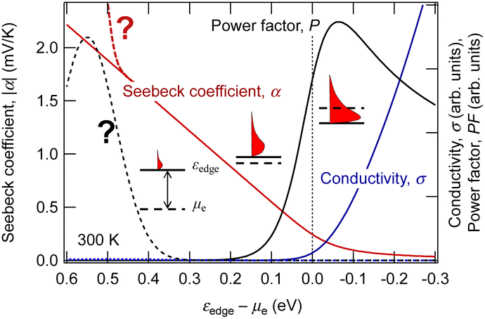 | ||
| Fig. 1 Dependence of electrical conductivity and Seebeck coefficient in three-dimensional semiconductors on the chemical potential of electrons calculated using eqn (2) and (3). | ||
Eqn (3) can be used as a general one for most materials regardless of them being a metal or semiconductor. Still, it is often transformed into more experiment-friendly formula using approximations that are considered reasonable on a case-by-case basis, especially in the field of material engineering. For example, by substituting the spectral conductivity of an ideal three-dimensional n-type semiconductor and using the Boltzmann approximation for fFD, one can obtain a Seebeck coefficient vs. conductivity equation,
 | (4) |
If the chemical potential of the electrons is far enough from the band edge, i.e., in the case of a near-intrinsic semiconductor with a wide band gap, we can further approximate eqn (4) as follows:
 | (5) |
This equation explicitly indicates that the Seebeck coefficient increases with increasing εc − μe or decreasing temperature. This also suggests that the Seebeck coefficient can be related to the entropy carried by a charge. If the Fermi energy is 1.5 eV away from the band edge, the Seebeck coefficient at 300 K reaches 5 mV K−1, which can be regarded as the upper limit of the Seebeck coefficient among practically available semiconductors if it follows the conventional linear response theory with the fluctuation–dissipation relation.
What is the giant Seebeck effect?
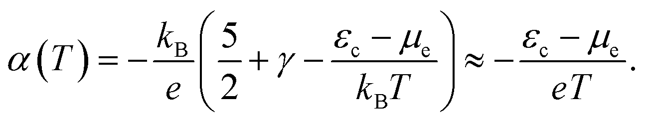
The GSE was first discovered in high-purity C60 thin films.5 In addition to the low electrical conductivity of the high-purity film, the sample resistance often exceeded 1 TΩ due to the in-plane sample geometry of the thin film. This discovery was made possible using an originally developed apparatus capable of in situ measurement of such a high-purity and high-resistance sample in an ultrahigh vacuum chamber.10 When impurity-doped C60 films were measured, the values followed the conventional theory as indicated by a red curve in Fig. 2. However, the Seebeck coefficients at 300 K obtained for pure C60 films were nearly 100-fold larger than the theoretical prediction as marked by a thick red circle.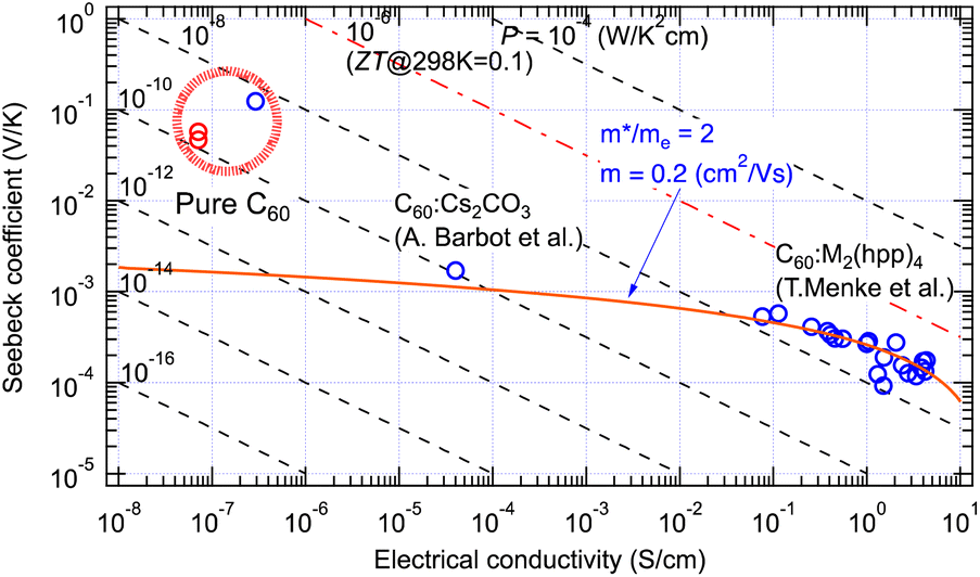 | ||
| Fig. 2 Seebeck coefficient and electrical conductivity of pure and doped C60 thin films measured at room temperature. The red curve indicates eqn (4) fitted to the results with doped C60 films.11,12 Red marks indicate positive Seebeck coefficients and blue ones negative. | ||
As explained in the previous section, these are improbable values if they must follow the conventional theory of the Seebeck effect. We, therefore, carefully performed confirmation experiments and discussed various possible factors to dispel any suspicion that it might be an artifact.
(1) Could it be due to a structural phase transition of the sample?
C60 is known to exhibit a phase transition related to the rotational motion of the molecule at around 260 K.13 A large Seebeck coefficient is often observed in a narrow temperature range across a phase transition temperature when the carrier transport properties change significantly.14 However, a differential scanning calorimetry (DSC) analysis of our C60 material showed no endothermic/exothermic peak at temperatures other than 260 K, confirming the absence of a structural phase transition in the temperature range of the thermopower measurement.5
(2) Could it be a temporary voltage due to some transient response in the sample?
If a sample contains a large number of mobile ions or trapped charges, their spatial distribution is rearranged when one side of the sample is heated, and the displacement current corresponding to the polarization change can be observed as a voltage in the measurement system. For example, it has been reported that a transient voltage called the ionic Seebeck effect due to the rearrangement of mobile ions was observed in poly(3,4-ethylenedioxythiophene) polystyrene sulfonate (PEDOT:PSS) thin films under high humidity conditions.15 However, even if the temperature difference (ΔT) was held for 40 minutes at each measurement step, a constant thermoelectromotive force (ΔV) corresponding to each ΔT was observed.5 Besides, the slopes of ΔV−ΔT characteristics were the same when the temperature difference was applied reciprocally. Thus, it was confirmed that what we measured was not a transient phenomenon.
(3) Are we measuring a false voltage caused by the input offset current of the measurement amplifier flowing through an ultra-high resistance sample?
Even with the most sophisticated differential amplifiers, achieving a completely zero input offset current between the positive and negative input terminals is difficult, and this input offset current would flow into an ultra-high resistance sample and generate a false voltage.16 For example, the operational amplifier used for the first stage of our amplifier has a typical input offset current of 20 fA,17 which produces an offset voltage of 0.2 V when the sample resistance is 10 TΩ. Since only the slope of the ΔV−ΔT characteristic is used in Seebeck coefficient measurements, the constant offset voltage is not a serious problem. However, if the sample resistance changes when a temperature difference is applied to the sample, the change of the offset voltage is added to the true ΔV, which causes an error in the Seebeck coefficient measurement.
To minimize this error factor, the average temperature of the sample in our instrument is kept constant when ΔT (<8 K) is applied to the sample, and the following method is used to periodically check for unexpectedly large input offset currents due to the deterioration of the amplifier: Two successive measurements are performed on the sample by exchanging the connections between the measurement amplifier and the sample where the direction of ΔT application is not changed. The polarity of the slope of the ΔV−ΔT characteristic must be opposite between the two measurements with swapped connections, but the absolute values must be equal. Since there have been no cases in which false Seebeck coefficients generated by the input offset current have been recognized by this test, it is believed that there is no such effect on the measured Seebeck coefficient in our experiments.
Universality of the giant Seebeck effect
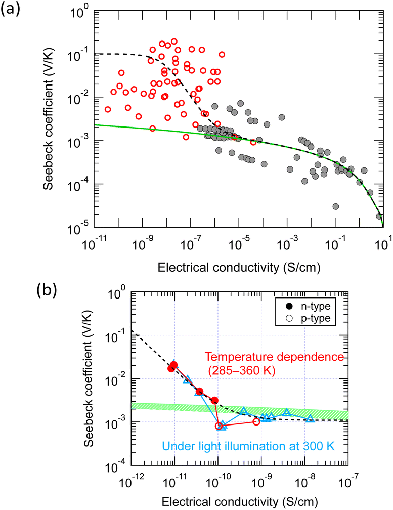
Fig. 3 shows the Seebeck coefficient and electrical conductivity of organic small-molecule semiconductors for more than 200 points measured by us since 2011 to date, including both thin films and single crystals, together with more than 100 points reported in the literature. The electrical conductivities reported by other research groups are distributed in the area >10−7 S cm−1 and their electrical conductivities and Seebeck coefficients are approximately within the area predicted by the conventional theory (green hatched area). From this, it can be concluded that the Seebeck effect of organic semiconductors can also be explained by the conventional theory in most cases. On the other hand, the values measured by us with high-purity semiconductors in ultra-high vacuum, distributed in a much lower conductivity range, frequently exhibited much larger Seebeck coefficients (surrounded by an orange frame) which cannot be explained by the conventional theory. | ||
| Fig. 3 Seebeck coefficient and electrical conductivity of various organic small-molecule semiconductors in the temperature range near 300–360 K. The green shaded area indicates the possible range of the values calculated from eqn (2) and (3). Red marks indicate positive Seebeck coefficients and blue ones negative. Filled marks are measured by the authors' group and transparent ones by other groups. The orange box indicates the area of the giant Seebeck effect. A table of values and reference information is available as ESI.† | ||
Initially, we thought that those exhibiting such giant Seebeck coefficients were rare. However, the GSE was observed in most of the high-purity small-molecule semiconductors, at least in part of the temperature range between 300 and 360 K. Therefore, it must be a universal phenomenon in high-purity small-molecule semiconductors. In the conductivity range of 10−5 S cm−1 or higher, there are a few materials that exhibited the normal Seebeck effect, but these are likely to be materials that could not be purified enough by the sublimation-purification technique.
The GSE is an interesting phenomenon in solid-state physics because it cannot be explained by the conventional theory in the textbooks. Not only that, it also has a big advantage for applications. When thermoelectric materials that follow the conventional theory of the Seebeck effect are used for power generation, the available Seebeck coefficient is around 0.1 mV K−1 because the amount of impurities is adjusted to reach the peak value of PF shown by the solid black line in Fig. 1. When such a material is used in wearable TEGs, the voltage obtained from a single stage of p-type or n-type material is at most 1 mV because the typical temperature difference is less than 10 K. Therefore, several hundreds of so-called π-type cells, consisting of a pair of p- and n-type, must be connected in series as shown in Fig. 4(a) to achieve 1 V or more output voltage, which is necessary for the subsequent voltage booster circuit to work efficiently.
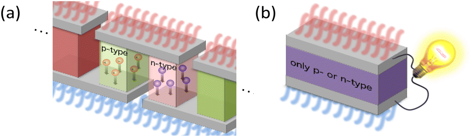 | ||
| Fig. 4 Illustration showing an advantage of the extremely large Seebeck coefficient for flexible TEGs: (a) a device using conventional thermoelectric materials and (b) that using a giant-Seebeck-effect material. | ||
In contrast, in the case of materials that exhibit the GSE, there is a new peak in PF when the Fermi level approaches the centre of the band gap, as shown by the black dotted line in Fig. 1. If this peak value is sufficiently high, output power can be generated even in such a low impurity region, and thus an extremely large Seebeck coefficient of around 0.1 V K−1, about 1000 times higher than that of conventional materials, can be used for power generation. As a result, as shown in Fig. 4b, a sheet-type TEG with an extremely simple structure, consisting of a single p- or n-type material sandwiched between electrodes, can be realized. This is a significant advantage for flexible applications.
Discussion on the possible origin of the giant Seebeck effect
As described above, it is already clear that the GSE is a steady-state phenomenon that appears in a wide range of high-purity small-molecule semiconductors, but its mechanism remains a mystery at this point. Here, we first consider whether GSEs have anything in common with other known phenomena.The phonon drag is a commonly known phenomenon that cannot be explained by the electron-only Boltzmann transport equation. Phonon flow due to the temperature gradient induces electron flow at low temperatures through electron–phonon scattering, which enhances Seebeck coefficients in some inorganic materials.18 The phonon-drag contribution gradually appears when the temperature goes down to the Debye temperature, TD, and becomes maximum at around TD/5. The TD of C60 in crystalline state is estimated in the range of 37–100 K,19 and thus the phonon drag should appear only at very low temperatures, <20 K. It would, therefore, be almost negligible in the temperature range of our experiments, 300–360 K.
As shown in eqn (5), the Seebeck coefficient can be regarded as the entropy carried by a charge. Substituting 0.1 V K−1 and 300 K, as typical values for the GSE, into eqn (5), we obtain εc − μe = 30 (eV), which means that the carrier is carrying energy that would be unthinkable with the conventional electron-only mechanism. It is, therefore, natural to assume that the electrons or holes do not carry this energy alone, and it is likely that phonons are involved in this phenomenon similarly to the phonon drag. However, the phonon drag is, in general, negligible at higher temperatures, whereas the GSE appears above 300 K. Therefore, the GSE cannot be explained by the concept of the phonon drag where momentum is transferred from phonons, having momentum in the temperature gradient direction, to low-temperature electrons in isotropic thermal motion.
Machida et al. reported that a “colossal Seebeck effect” appears in a quasi-one-dimensional organic conductor, (TMTSF)2PF6, at less than 10 K.20 The maximum value of the measured Seebeck coefficient was of the same order as those appearing in the GSE in this work. According to their explanation, this phenomenon is related to the difference in temperature dependence between related quantities. In an insulator (or a semiconductor in a practical sense), the average thermal energy of a carrier is temperature-independent and determined by the energy difference between the electron chemical potential and the closest transport level. Under such a condition where both the carrier number and entropy vanish at 0 K, the Seebeck coefficient increases with decreasing temperature if the carrier number decreases faster. However, the theoretical prediction becomes difficult because the transport in such a low-temperature limit becomes trap-limited variable range hopping (VRH). In their experiment, the electrical conductivity followed the theoretical temperature dependence of d-dimension VRH,
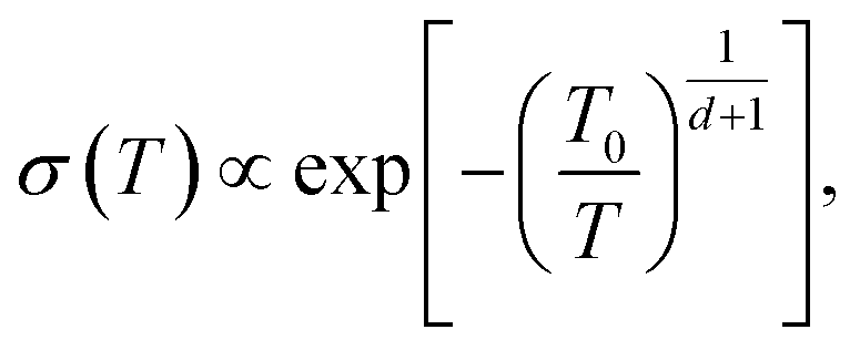 | (6) |
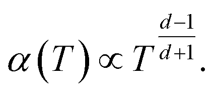 | (7) |
It is unclear whether the above discussion should be considered in the mechanism of the GSE. At this time, however, what should be considered most is the small polarons, in which electrons and lattices are strongly coupled. In that case, the linear response theory with the fluctuation–dissipation relation no longer applies. We have tried to numerically solve the Schrödinger equation using a Hamiltonian describing a small polaron with material parameters corresponding to pentacene and obtained the Seebeck coefficient by the Kubo formula. The preliminary result indicated that the giant Seebeck coefficient of several tens of mV K−1 was reproduced with this method.23 However, it is premature to say that small polaron alone can explain the GSE, since experimental results are often not perfectly explained.
In the following, we further report some important but fragmented findings from our unpublished data to elucidate the mechanism and necessary conditions of the GSE with the help of the scientific community. Although each experimental fact alone does not provide sufficient information to identify the mechanism of the GSE, we hope that the essence of the GSE can be revealed by collecting various characteristics.
Facts and discussions related to the giant Seebeck effect
Does the GSE appear in single crystals?
The thermoelectric properties of single crystals of PDI, for which the GSE was not obtained in thin films,6 BP, for which it was obtained,6 and rubrene, which is difficult to measure in the thin film state because of its amorphous nature, were evaluated in an ultrahigh vacuum by supporting both ends of the single crystals with thin gold wires to avoid stress due to thermal expansion. As seen in Fig. 5, all single crystals showed giant Seebeck coefficients. Their temperature dependence is more straightforward than that obtained with thin films and tends to decay by elevating temperature. The complex temperature dependence in thin films may include the contribution of the changes in molecular packing due to the thermal expansion under friction by the substrates.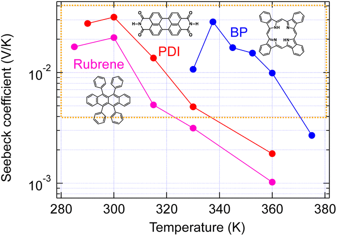 | ||
| Fig. 5 Temperature dependence of Seebeck coefficient measured with organic single crystals. The orange box indicates the area of the giant Seebeck effect. | ||
Why does the GSE not appear in high electrical conductivity region?
As shown in Fig. 3, the GSE has not been observed so far in the conductivity region above 10−5 S cm−1. In a system where two conduction mechanisms coexist, the average Seebeck coefficient weighted by the conductivity of each mechanism is measured as in the following equation: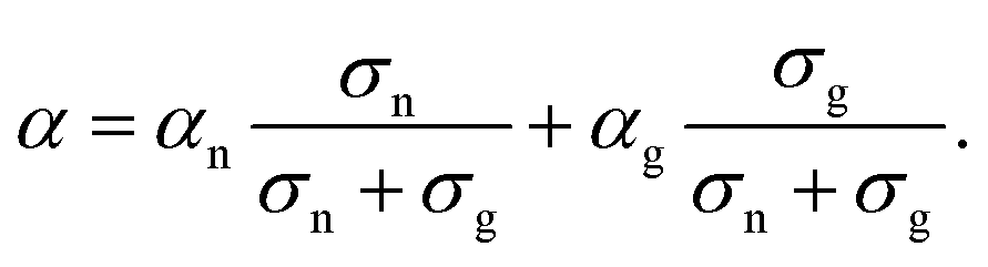 | (8) |
 | ||
| Fig. 6 Fitting of the two-band model equation [eqn (8)] to the experimental results: (a) a general trend with various small-molecule semiconductors and (b) results obtained with a rubrene single crystal by changing temperature or light intensity. The model contains two independent transport mechanisms: a giant Seebeck coefficient with constant electrical conductivity and a normal Seebeck coefficient with variable electrical conductivity. | ||
Then, what are the possible two conduction mechanisms that coexist in a single material? For example, a possible case is that most carriers are trapped, and conduction becomes VRH-like at a low carrier density limit, as seen in (TMTSF)2PF6. Another possibility is that there are no specific traps but energy fluctuations at the band edge. Most carriers exist at the bottom of the fluctuation valley at a low carrier density limit. However, as carrier density increases, the ratio of carriers with energy beyond the top of the fluctuation increases, and conduction changes from hopping-like to band-like.
Fig. 7a and b show a conceptual depiction of the carrier distribution at low and high carrier densities on the measured band edge fluctuation profiles in pentacene thin films,24,25 respectively. Since pentacene is also a high carrier mobility semiconductor that exhibits band transport within the crystal, it is easy to infer that the conventional Seebeck effect due to the band transport is observed in the state shown in Fig. 7b. On the other hand, when most carriers exist at the bottom of the fluctuating valley, as shown in Fig. 7a, the state is intermediate between the multiple-trapping-and-release and the band transport. Such a weakly confined state may be necessary for the emergence of a GSE.
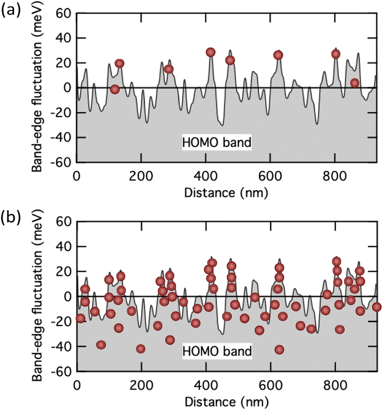 | ||
| Fig. 7 Schematic illustration showing the distribution of carriers near a fluctuated HOMO band edge at (a) low and (b) high carrier concentration states. The band edge profile is taken from the experimental one measured with pentacene polycrystalline films.24 | ||
Assuming that the conductivity at the transition from the GSE to the normal Seebeck effect in the various thin films in Fig. 6a is approximately 10−7 S cm−1, the carrier density converted by a typical carrier mobility (0.1 cm2 V−1 s−1) is about 6 × 1012 cm−3. If the transition conductivity is 10−11 S cm−1 in Fig. 6b, the carrier density converted by a typical carrier mobility (10 cm2 V−1 s−1) is surprisingly small, only about 3 × 106 cm−3. If this is the density of structures directly involved in the mechanism of the GSE, it would be tough to identify such trace amounts of traps by elemental or structural analyses.
Does the GSE appear in powder samples?
If the GSE is also observed in powder samples, experiments to screen promising materials would be much more efficient and faster. Therefore, we measured the TE properties of powder pellets in air for which the GSE was observed in the thin film or crystalline state. However, none of the tested samples exhibited the GSE (marked by circles in Fig. 8). Although the electrical conductivity of the high-purity thin films and the powder pellets are at the same level, the carrier density seems to be 4 to 7 orders of magnitude higher than that of the thin film samples due to the low mobility characteristic of powder pellets. This may prevent the emergence of the GSE, even if the intrinsic GSE mechanism still exists, as discussed for the results in Fig. 6.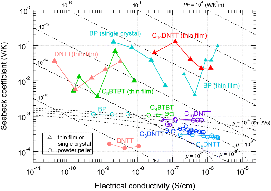 | ||
| Fig. 8 Seebeck coefficient and electrical conductivity of various organic materials in (triangles) thin film/single crystal states and (circles) powder pellets. The temperature is within 300–360 K. The dash-dotted curves indicate the theoretical α–σ relation calculated from eqn (4) by assuming various carrier mobilities. | ||
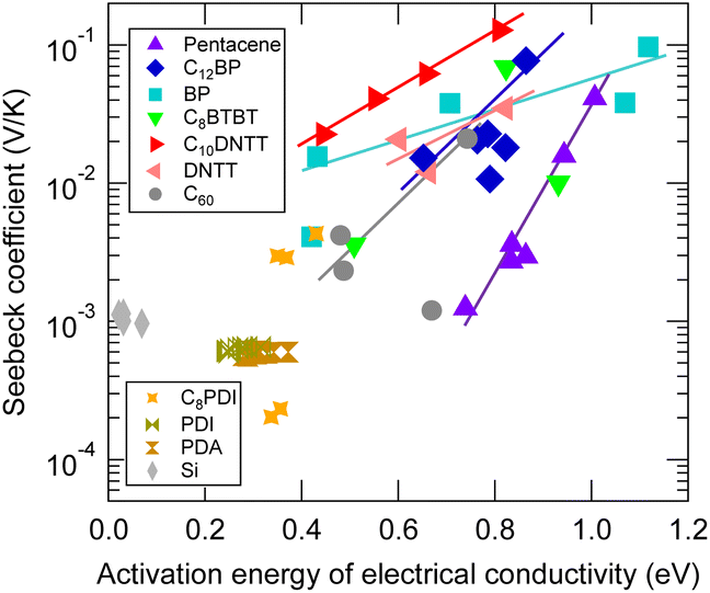
Proportionality of log Seebeck coefficient and activation energy of electrical conductivity
Materials that exhibit a GSE often have large activation energies of conductivity of approximately 0.4 eV or more, and a positive correlation is often observed between the logarithm of the Seebeck coefficient and the differential activation energy at the same temperature, when temperature is varied.6These activation energies are also highly temperature dependent and cannot be attributed to the HOMO–LUMO interband electronic transition. Although the reorganization energy (or polaron hopping energy) of the hopping transport may also appear to be an Arrhenius-type activation energy in the narrow temperature range, the values of activation energy seen in Fig. 9, which is around 1 eV when the Seebeck coefficient is giant, are much larger than the reorganization energy calculated for these organic semiconductors. Whether these large activation energies can be attributed to trap depth or not is not known at this time. However, their existence cannot be ruled out since little work has been done on traps which have a density at the ppt level as estimated in the previous section.
 | ||
| Fig. 9 Relationship between Seebeck coefficient and activation energy of electrical conductivity in the same temperature range. The same symbols indicate those measured with the same sample but at different temperatures. | ||
Dependence of electrical conductivity and Seebeck coefficient on temperature and heteroatom substitution
Fig. 10 shows the temperature dependence of conductivity and Seebeck coefficient measured with single crystals of six different molecules obtained by substituting hetero elements at several locations in the equivalent molecular skeleton [inset of Fig. 10a]. It is difficult to identify the conduction mechanism from the wide range of temperature dependence in high-purity organic thin films and single crystals because the measurable temperature range is often narrow due to conductivity decreases on the low-temperature side and evaporation or melting of the sample on the high-temperature side. Furthermore, the large random errors in the measurements also make precise analysis difficult. However, since the results in Fig. 10 have relatively small random errors and their temperature dependences are monotonic, we will discuss the carrier transport mechanism from these results.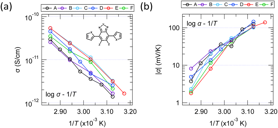 | ||
| Fig. 10 Temperature dependence of the (a) electrical conductivities and (b) Seebeck coefficients of six molecules having the same molecular skeleton shape but different heteroatoms. | ||
The fact that the log![[thin space (1/6-em)]](https://www.rsc.org/images/entities/char_2009.gif) σ–1/T plot is relatively linear in this temperature range suggests that the conductivity is most likely of the Arrhenius type rather than the VRH type. Of course, it is also quite possible that this can be explained by the Holstein hopping model within a narrow temperature range. On the other hand, while many thin films show complex behaviour in the Seebeck coefficient with temperature (e.g., upper half in Fig. 8), the results in Fig. 10 show a relatively monotonic variation. However, it was not perfectly straight in any of the various plots commonly seen in studies on transport phenomena (e.g., logα–logT plots, logα–Tr plots with various exponents, etc.). Therefore, the similarity to the phenomenon observed with (TMTSF)2PF6 at a cryogenic temperature (introduced in a previous section) seems to be low. As we attempted a rough analysis in Fig. 6, it is quite probable that we are not observing a temperature dependence of the GSE itself in this temperature range, but rather a transition between different charge transport mechanisms due to changes in carrier density.
σ–1/T plot is relatively linear in this temperature range suggests that the conductivity is most likely of the Arrhenius type rather than the VRH type. Of course, it is also quite possible that this can be explained by the Holstein hopping model within a narrow temperature range. On the other hand, while many thin films show complex behaviour in the Seebeck coefficient with temperature (e.g., upper half in Fig. 8), the results in Fig. 10 show a relatively monotonic variation. However, it was not perfectly straight in any of the various plots commonly seen in studies on transport phenomena (e.g., logα–logT plots, logα–Tr plots with various exponents, etc.). Therefore, the similarity to the phenomenon observed with (TMTSF)2PF6 at a cryogenic temperature (introduced in a previous section) seems to be low. As we attempted a rough analysis in Fig. 6, it is quite probable that we are not observing a temperature dependence of the GSE itself in this temperature range, but rather a transition between different charge transport mechanisms due to changes in carrier density.
Substitution of heteroatoms in a conjugated system often changes the HOMO and LUMO energies, as well as the intermolecular transfer integral, which is generally sensitive to slight changes in packing, resulting in a notable variation of carrier mobility. Although not a large difference, the difference in conductivity among the different molecules in Fig. 10a is most likely due to such a change in the transfer integral. On the other hand, while there exists a relatively wide variation of the Seebeck coefficient among molecules for the conventional Seebeck effect at the higher temperature, the difference almost disappears at the lower temperature where the GSE appears. This suggests that the GSE is relatively insensitive to heteroatoms and the resulting transfer integral.
Conclusions
We discovered the GSE about 10 years ago and have been studying it steadily. However, we have not yet fully understood the nature of the phenomenon. This paper reported an overview of the GSE, conventional theories and similar phenomena that should be considered, and some unpublished experimental facts we have obtained so far that may contribute to understanding the mechanism and necessary conditions of the GSE. The GSE frequently appears in high-purity organic semiconductors and is a reproducible phenomenon that is not a transient one or an artifact. However, the phenomenon has not been observed in samples with high carrier density, and it is still inconclusive as to whether it is an essential phenomenon related to standard charge and heat transport processes in organic semiconductors, or whether it is a phenomenon that requires the involvement of a specific structure that is universal but infrequent, such as carrier traps or deep valleys of the potential fluctuations. We hope that sharing the results and discussions in this paper with the scientific community will advance our understanding of this phenomenon.Author contributions
M. Nakamura conceived the basic idea, designed the special instruments used in this work, and supervised the entire research. H. Kojima, R. Abe, and Y. Cho carried out the experiments and calculations by guiding many students. S. Hayashi synthesized special molecules measured in Fig. 10. M. Hiramoto prepared high-purity rubrene single crystals. The manuscript has been prepared by M. Nakamura. All authors have approved the final version of the manuscript.Conflicts of interest
There are no conflicts to declare.Acknowledgements
This work was supported by JSPS KAKENHI Grant Numbers 25888016, 15K21163, 15H01000, 17H05158 and 21H02013. MN, HK, and SH particularly thank a Grant-in-Aid for Scientific Research on Innovative Areas ‘‘π-System Figuration: Control of Electron and Structural Dynamism for Innovative Functions’’ (26102002) for the fruitful discussion and encouragement of collaborations among the area members. The authors wish to thank all the collaborators and the students who worked on this more than ten years study: Profs H. Yamada (Kyoto U.), D. Kuzuhara, N. Yoshimoto (Iwate U.), Y. Yakiyama, H. Sakurai (Osaka U.), R. Matsubara (Shizuoka U.), Drs T. Yamamoto, H. Yakushiji, M. Ikeda (Nippon Kayaku), M. Ito (Furukawa Electric), T. J. Inagaki, Messrs. A. Hoshi, Y. Tomatsu, F. Fujiwara, M. Nakagawa, T. Takeuchi, S. Inoue. K. Kojima, T. Kawauchi, T. Sugiyama, S. Hattori, T. Kimura, and H. Kimura.References
- V. Leonov and R. J. M. Vullers, J. Renewable Sustainable Energy, 2009, 1, 062701 CrossRef.
- G. Xu, Y. Yang, Y. Zhou and J. Liu, Front. Energy, 2013, 7, 26 CrossRef.
- T. J. Seebeck, Abhandlungen der Königlichen Akademie der Wissenschaften zu Berlin, 1822, 265 Search PubMed.
- For example, R. E. Howard and A. B. Lidiard, Discuss. Faraday Soc., 1957, 23, 113 RSC; R. Schneebaum and B. R. Sundheim, Discuss. Faraday Soc., 1961, 32, 197 RSC; A. R. Blythe, M. R. Boon and P. G. Wright, Discuss. Faraday Soc., 1971, 51, 110 RSC.
- H. Kojima, R. Abe, M. Ito, Y. Tomatsu, F. Fujiwara, R. Matsubara, N. Yoshimoto and M. Nakamura, Appl. Phys. Express, 2015, 8, 121301 CrossRef.
- H. Kojima, R. Abe, F. Fujiwara, M. Nakagawa, K. Takahashi, D. Kuzuhara, H. Yamada, Y. Yakiyama, H. Sakurai, T. Yamamoto, H. Yakushiji, M. Ikeda and M. Nakamura, Mater. Chem. Front., 2018, 2, 1276 RSC.
- H. Kojima, M. Nakagawa, R. Abe, F. Fujiwara, Y. Yakiyama, H. Sakurai and M. Nakamura, Chem. Lett., 2018, 47, 524 CrossRef CAS.
- For example, G. Mahan, Many-Particle Physics, Kluwer Academic, New York, 1981 Search PubMed.
- T. Takeuchi, Mater. Trans., 2009, 50, 2359 CrossRef CAS.
- M. Nakamura, A. Hoshi, M. Sakai and K. Kudo, Mater. Res. Soc. Symp. Proc., 2009, 1197, 72 CrossRef.
- A. Barbot, C. D. Bin, B. Lucas, B. Ratier and M. Aldissi, J. Mater. Sci., 2013, 48, 2785 CrossRef CAS.
- T. Menke, D. Ray, J. Meiss, K. Leo and M. Riede, Appl. Phys. Lett., 2012, 100, 093304 CrossRef.
- K. Horiuchi, S. Uchino, K. Nakada, N. Aoki, M. Shimizu and Y. Ochiai, Phys. B, 2003, 329–333, 1538 CrossRef CAS.
- T. Mori, H. Inokuchi, A. Kobayashi, R. Kato and H. Kobayashi, Phys. Rev. B: Condens. Matter Mater. Phys., 1988, 38, 5913 CrossRef CAS PubMed.
- H. Wang, U. Ail, R. Gabrielsson, M. Berggren and X. Crispin, Adv. Energy Mater., 2015, 5, 1500044 CrossRef.
- Please see a tutorial document provided by Analog Devices, MT-038, https://www.analog.com/media/en/training-seminars/tutorials/MT-038.pdf.
- Please see the AD549 datasheet provided by Analog Devices, https://www.analog.com/media/en/technical-documentation/data-sheets/ad549.pdf.
- For example, I. Weinberg, Phys. Rev., 1965, 139, A838 CrossRef; S. M. Puri, Phys. Rev., 1965, 139, A995 CrossRef.
- V. P. Mikhal’chenko, Phys. Solid State, 2010, 52, 1549 CrossRef.
- Y. Machida, X. Lin, W. Kang, K. Izawa and K. Behnia, Phys. Rev. Lett., 2016, 116, 087003 CrossRef.
- M. J. Burns and P. M. Chaikin, J. Phys. C, 1985, 18, L743 CrossRef CAS.
- N. Lu, L. Li, W. Banerjee, P. Sun, N. O. Gao and M. Liu, J. Appl. Phys., 2015, 118, 045701 CrossRef.
- T. J. Inagaki, H. Kojima and M. Nakamura, 7th International Symposium on π-System Figuration, Osaka, Japan, 29 March, 2019, p. 68; and private communication with Dr T. J. Inagaki Search PubMed.
- N. Ohashi, H. Tomii, R. Matsubara, M. Sakai, K. Kudo and M. Nakamura, Appl. Phys. Lett., 2007, 91, 162105 CrossRef.
- R. Matsubara, Y. Sakai, T. Nomura, M. Sakai, K. Kudo, Y. Majima, D. Knipp and M. Nakamura, J. Appl. Phys., 2015, 118, 175502 CrossRef.
Footnote |
| † Electronic supplementary information (ESI) available: Table including references for Fig. 3. See DOI: https://doi.org/10.1039/d3fd00127j |
| This journal is © The Royal Society of Chemistry 2024 |