
 Open Access Article
 This Open Access Article is licensed under a Creative Commons Attribution-Non Commercial 3.0 Unported Licence
Thermal deformation of gold nanostructures and its influence on surface plasmon resonance sensing†
Hyun-Tae
Kim
 ,
Mayank
Pathak
,
Keshav
Rajasekaran
,
Ashwani K.
Gupta
and
Miao
Yu
*
,
Mayank
Pathak
,
Keshav
Rajasekaran
,
Ashwani K.
Gupta
and
Miao
Yu
*
Department of Mechanical Engineering, University of Maryland, College Park, Maryland 20742, USA. E-mail: mmyu@umd.edu
First published on 27th December 2019
Abstract
Plasmonic nanostructures have been recently used in elevated temperature applications such as sensing of high-energy systems and localized heat generation for heat-assisted magnetic recording, thermophotovaltaics, and photothermal therapy. However, plasmonic nanostructures exposed to elevated temperature often experience permanent deformations, which could significantly degrade performance of the plasmonic devices. Therefore, understanding of thermal deformation of plasmonic nanostructures and its influence on the device performance is essential to the development of robust high-performance plasmonic devices. Here, we report thermal deformation of lithographic planar gold nanopatch and nanohole arrays and its influence on surface plasmon resonance sensing. The gold nanostructures are fabricated on a silicon substrate and on the end-face of an optical fiber using electron-beam lithography and focused-ion-beam lithography, respectively. The fabricated gold nanostructures are exposed to cyclic thermal loading in the range of 25 °C to 500 °C. Through experimental and numerical studies, we investigate (i) thermal deformation modes of the gold nanostructures, (ii) influence of the gold nanostructure geometry on the degree and mechanism of the thermal deformation, and (iii) influence of the thermal deformation on performance of surface plasmon resonance sensing. The obtained understanding from these studies is expected to help guide the development of robust high-performance plasmonic sensors for monitoring in elevated temperature environments. Although the current work is focused on gold nanostructures, it can be extended to provide useful insights on thermal deformation of refractory plasmonic nanostructures at extreme temperature.
1. Introduction
Plasmonic nanostructures, such as metallic nanorods, nanoshells, nanopatches, and nanoholes, which can effectively excite localized surface plasmons (LSPs) and surface plasmon polaritons (SPPs), have received much attention in various applications.1–7 Recently, these nanostructures have been employed in elevated temperature applications, including (i) plasmonic sensing (e.g., temperature and gas) of high-energy systems (500–900 °C) such as combustors, gas turbines, and solid-state fuel cells8–10 and (ii) generation of localized heat11,12 for heat-assisted magnetic recording (∼350 °C),13 thermophotovaltaics (∼1000 °C),14 and photothermal therapy (∼80 °C).15 At such elevated temperature, understanding of the thermal deformation of plasmonic nanostructures is important in the design and operation of plasmonic devices since the nanostructure geometry, along with the temperature-dependent optical properties of plasmonic materials,16–18 determines the important device performance characteristics such as resonance wavelength, Q-factor, and electric field intensity at resonance.3,11,19,20 Therefore, investigations into thermal deformation of plasmonic nanostructures and its influence on the performance-related characteristics is essential to the development of robust, high-performance plasmonic devices for elevated temperature operation.There have been a number of efforts devoted to investigate thermal deformation of plasmonic nanostructures either in elevated temperature environments or under high-power laser irradiation. For example, capillarity-driven thermal deformation of various aspect-ratios of colloidal-like gold (Au) nanorods was investigated.21,22 Furthermore, changes in LSP resonance (LSPR) of colloidal-like Au nanorods due to thermal deformation were reported.23,24 In another effort, thermal deformations of lithographic planar nanorings with two different materials (Au and titanium nitride) and resulting changes in LSPR were compared.25 On the other hand, it was reported that dielectric coating of Au nanostructures can suppress their thermal deformation.9,26,27 However, for lithographic planar nanostructures, influence of the nanostructure geometry on the thermal deformation and resulting changes in surface plasmon resonance (SPR) have not been investigated.
In this paper, we report thermal deformation of lithographic planar Au nanopatch and nanohole arrays under cyclic thermal loading and its influence on the SPR sensing. In particular, the influence of the nanostructure geometry on the degree and mechanism of the thermal deformation is investigated with various Au nanopatch and nanohole arrays fabricated on a silicon (Si) substrate. Furthermore, the influence of the thermal deformation on the SPR based sensing is characterized. Additionally, as a potential application for on-fiber SPR sensing, thermal deformation of Au nanopatch arrays fabricated on the end face of a single-mode optical fiber and the resulting changes in the SPR are investigated. It should be noted that we use Au as a plasmonic material despite its relatively low melting temperature (1063 °C) since it renders excellent plasmonic properties even at elevated temperature. The SPP propagation length and Q-factor of LSPR of Au nanostructures have been reported to be better than those of refractory plasmonic nanostructures (e.g., titanium nitride nanostructures) at a temperature up to 500 °C.17 Therefore, Au plasmonic nanostructures are an attractive choice for moderately high temperature applications. On the other hand, the obtained understanding from Au nanostructures can provide useful insights into thermal deformation and the resulting SPR performance changes of other refractory plasmonic nanostructures at extreme temperature.
2. Results and discussion
2.1 Au nanostructures on Si substrate
Au nanopatch and nanohole arrays of different geometric parameters (shape and size) were fabricated on a Si substrate using electron-beam (e-beam) lithography. The nanostructures were defined on a 60 nm thick Au film on top of a 1 μm thick silicon dioxide (SiO2) layer with a 3 nm of titanium (Ti) adhesion layer [Fig. 1a]. Fig. 1b shows scanning electron microscopy (SEM) images of representative unit cells of all the fabricated Au nanostructures. Square and circular shaped patterns were used to design the nanopatch and nanohole arrays. For each shape, three different widths (W = 500 nm, 800 nm, 1000 nm) of patterns were designed with either a constant periodicity (P = 1100 nm) or a constant gap (P − W = 300 nm). Note that the fabricated nanopatch (and nanohole) sizes are slightly larger (and smaller) than the design values, which is due to over-exposure of the e-beam resist. The array footprint was designed to 100 μm × 100 μm for all the nanostructures. Fig. 1c and d show SEM images of the fabricated square Au nanopatch and nanohole arrays with W = 800 nm and P = 1100 nm, respectively.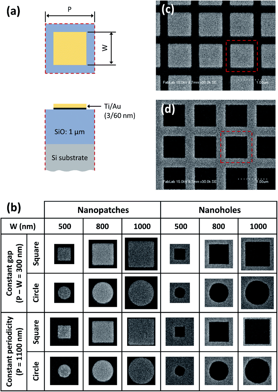 | ||
| Fig. 1 (a) Top and cross-sectional views of the unit cell of a square Au nanopatch array. (b) SEM images of representative unit cells of all the fabricated Au nanopatch and nanohole arrays with design values of W and P. SEM images of the fabricated square Au (c) nanopatch and (d) nanohole arrays with W = 800 nm and P = 1100 nm (red-dashed box indicates a unit cell). | ||
2.2 Thermal deformation modes of Au nanostructures
The fabricated Au nanostructures were exposed to cyclic thermal loading in the temperature range from 25 °C to 500 °C. Under the cyclic thermal loading, the Au nanostructures experienced evolutions of the pattern geometry and surface morphology. Fig. 2a shows SEM images of representative unit cells of the square Au nanopatch and nanohole arrays (W = 800 nm, P = 1100 nm) before thermal loading and after 200, 400, 700, 1000, 1500, and 2000 cycles of thermal loading. As shown in the SEM images, the corners and edges of the square patterns became blunted with increasing thermal loading cycles. At the same time, the measured pattern area of the square nanopatch (and nanohole) array decreased (and increased), as shown in Fig. 2b and c. In particular, the pattern geometry evolution occurred drastically within the initial 200 cycles of thermal loading and then the pattern became stabilized after approximately 700 cycles. On the other hand, large Au lumps emerged from the surfaces of the nanostructure, as shown in Fig. 2d and e. These evolutions of the pattern geometry and surface morphology were observed in all other fabricated Au nanostructures of various other shapes and sizes [see Fig. S1†].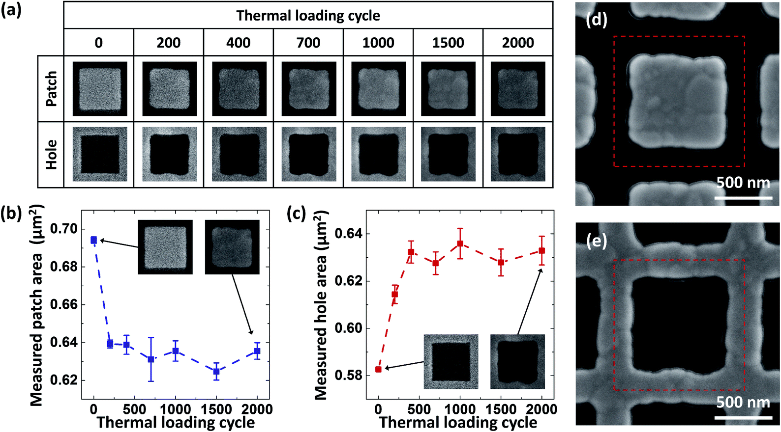 | ||
| Fig. 2 (a) SEM images of representative unit cells of square Au nanopatch and nanohole arrays (W = 800 nm, P = 1100 nm) before thermal loading and after 200, 400, 700, 1000, 1500, and 2000 cycles of thermal loading. The measured pattern areas of the square Au (b) nanopatch and (c) nanohole arrays (W = 800 nm, P = 1100 nm) after each thermal loading cycle. High-resolution SEM images of the square Au (d) nanopatch and (e) nanohole arrays (W = 800 nm, P = 1100 nm) after 2000 cycles of thermal loading (red-dashed box indicates a unit cell). | ||
The observed thermal deformation is mainly attributed to the interface (i.e., surface and grain boundary) diffusion of Au atoms under capillarity forces and surface stress.28 Note that such thin-film nanostructures often have small-sized grains,29 where dislocation-based deformation is suppressed.30 At elevated temperature, the diffusion is facilitated since the diffusivity increases with increasing temperature according to the Arrhenius relation.21 The capillarity-induced surface diffusion, which minimizes the surface free energy of the nanostructures, blunts the corners and edges of the Au nanostructures and decreases the pattern area of the nanopatch array (and increases the pattern area of the nanohole array), as shown in Fig. 3a. Similar examples of capillarity-induced deformations were reported in the literature, including blunting of field emission tips31 and reduction of the aspect ratio of nanorods.21 On the other hand, compressive/tensile stress is developed on the Au nanostructures under cyclic thermal loading due to the coefficient of thermal expansion (CTE) mismatch between the Au nanostructure and SiO2/Si substrate [Fig. 3b]. The stress gradient over the Au grains is relaxed by grain boundary diffusion,32 which leads to grain boundary migration, grain boundary sliding, and grain rotation, and grain growth.30 These grain motions induce the pattern boundary deformation and large Au lumps on the nanostructure surface.30,32 In particular, the nanohole arrays could be more vulnerable to the pattern boundary deformation than the nanopatch arrays since high thermal stresses are concentrated on the pattern boundary (point B in Fig. 3d) for the nanohole arrays but in the pattern center for the nanopatch arrays (point A in Fig. 3c). It should be noted that thermal fatigue damages such as hillocks and voids have been reported for nanostructures under long-term thermal loading.32 However, for the fabricated Au nanostructures, only a few hillocks and voids were observed in the entire nanostructures after 2000 cycles of thermal loading [Fig. 3e and f]. It should be noted that the stress state of the Au film during deposition also contributes to the stress-induced diffusion, which it is not analyzed in this work.
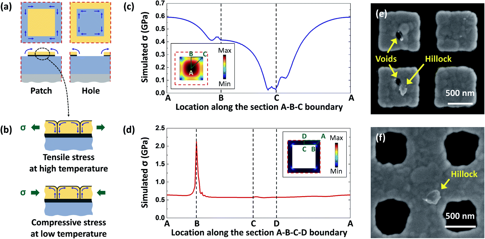 | ||
| Fig. 3 Schematics showing thermal deformation of the Au nanostructures by (a) capillarity-induced surface diffusion and (b) stress-induced grain boundary diffusion: blue arrows indicate the interface diffusion of Au atoms. Simulated thermal stresses along the section boundary of the unit cell square Au (c) nanopatch and (d) nanohole arrays (W = 800 nm, P = 1100 nm). The insets show the 2D thermal stress profiles of the unit cell Au nanostructures and selected section boundary (three points A, B, C were selected for nanopatch and four points A, B, C, D were selected for nanohole arrays). High-resolution SEM images showing the thermal fatigue damages on the square Au (e) nanopatch (W = 800 nm, P = 1100 nm) and (f) nanohole (W = 500 nm, P = 1100 nm) arrays after 2000 cycles of thermal loading. | ||
2.3 Influence of Au nanostructure geometry on thermal deformation
The degree and mechanism of the thermal deformation were investigated based on the normalized pattern area change (ΔA/A0) and simulated thermal stress (σ) of the various geometries of Au nanostructures. Note that ΔA is the measured pattern area change (obtained from 700 to 2000 thermal loading cycles) and A0 is the initial pattern area measured before thermal loading.For the nanopatch arrays, ΔA/A0 is almost a constant around 0.10, which slightly increases with decreasing A0 (i.e., smaller patterns suffer slightly larger normalized area change) [Fig. 4a]. On the other hand, the simulated stress level decreases with decreasing patch area and the patch boundary experiences lower stress than the inner area [Fig. 4c]. Considering the negative correlation between the ΔA/A0 and A0, positive correlation between the stress level and patch area, and 2D thermal stress profile, capillarity is believed to be a dominant driving force for the geometry changes of the nanopatch arrays over thermal stress. Furthermore, for the nanopatches with a fixed W, ΔA/A0 is independent of the gap size between the adjacent nanopatches. ΔA/A0 is almost not influenced by the shape of the nanopatch [Fig. 4a].
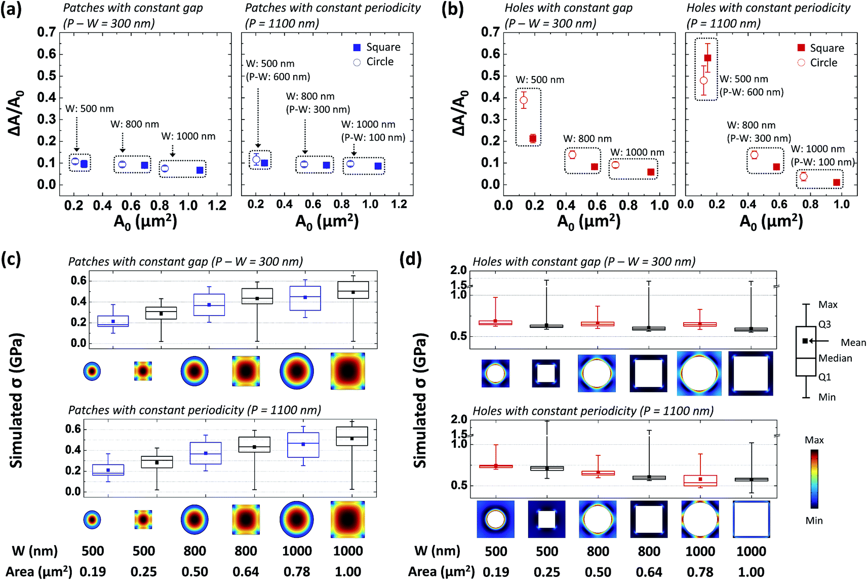 | ||
| Fig. 4 ΔA/A0 as a function of A0 for the fabricated Au (a) nanopatch and (b) nanohole arrays with various shapes and sizes (constant gap on the left and constant periodicity on the right). The dashed box groups the two different pattern shapes with same geometry. Simulated thermal stress levels and 2D thermal stress profiles of the unit cell Au (c) nanopatch and (d) nanohole arrays with various shapes and sizes (constant gap on the top and constant periodicity on the bottom). ΔA/A0 and A0 are measured values and W, P, and area are design values. Simulation temperature is 500 °C. | ||
The nanohole arrays exhibit different thermal deformation trend from the nanopatch arrays, which indicates a different deformation mechanism. For the same shape of nanohole arrays, ΔA/A0 drastically increases with decreasing A0 [Fig. 4b]. On the other hand, the simulated stress level increases with decreasing A0 and high stresses are concentrated around the hole boundary [Fig. 4d] (see Fig. S2 and S3 in the ESI† for better comparison of nanohole arrays of the same shape). Further, compared with the same shape and size of nanopatch arrays, the nanohole arrays have a higher stress level. Based on the strong negative correlation between the ΔA/A0 and A0, negative correlation between the stress level and hole area, and 2D thermal stress profile, thermal stress is believed to be a dominant driving force for the geometry changes of the nanohole arrays over capillarity. Furthermore, for the nanoholes with a fixed W, a larger gap size between the adjacent nanoholes induces a larger ΔA/A0, which is attributed to a higher stress level of the nanohole array with a larger gap. The nanohole shape has an influence on ΔA/A0 [Fig. 4b]. This can be attributed to a slightly higher stress level (i.e., mean, median, and Q1/Q3 values) of the circular nanoholes.
2.4 Influence of thermal deformation on SPR sensing
Finite-difference time-domain (FDTD) simulations were performed to investigate the influence of the thermal deformation of the Au nanostructures on SPR sensing. Two Au nanostructure designs were simulated with 3D unit cell models: a square nanopatch array (W = 1000 nm, P = 1100 nm, duty cycle = 90%) [Fig. 5a] and circular nanohole array (W = 500 nm, P = 1100 nm, duty cycle = 45%) [Fig. 5b]. Note that these two designs were chosen here because they offer better SPRs compared with other geometric designs (see Fig. S4† for simulation results of other Au nanostructure designs). These nanostructure geometries have been used for SPR sensing. For example, square nanopatch arrays with a high duty-cycle were recently reported for Rayleigh anomaly (RA)-based sensing,33 and circular nanohole arrays with around 45% of duty-cycle were used for SPP-based sensing.34Fig. 5c and d show the simulated reflection spectra of the square nanopatch array and circular nanohole array, respectively, before thermal loading and after 2000 thermal loading cycles. Note that the W for the simulation models is an equivalent width calculated from the measured area of the fabricated nanostructures before and after thermal loading. The resonance dip around 1590 nm obtained from the square nanopatch array represents RA [Fig. 5c inset], and the resonance dip around 1650 nm from the circular nanohole array represents SPP [Fig. 5d inset]. The changes in the resonance profiles before and after thermal loading were analyzed in terms of three metrics related to SPR sensing: a resonance wavelength (λres), full-width half-maximum (FWHM) of the resonance, and extinction of the reflection at the λres (Extres), as shown in Table 1. For the λres and FWHM, the square nanopatch array is much more robust to the thermal deformation than the circular nanohole array; the changes in λres and FWHM (i.e., |Δλres| and ΔFWHM) for the square nanopatch array are 3.6% and 4.7% of those for the circular nanohole array, respectively. On the other hand, the changes in Extres (i.e., |ΔExtres|) are on the same magnitude for both arrays (Extres for nanohole array slightly increases, while it slightly decreases for nanopatch array). These changes, if not properly compensated, could significantly degrade the SPR sensing performance. For example, a shift in λres could degrade the sensing accuracy for wavelength-modulated sensing modalities. Furthermore, for intensity-modulated sensing modalities using a probe laser wavelength located at the FWHM point, the ΔFWHM and ΔExtres would change the sensitivity and dynamic range. It should be noted that the on-substrate Au nanostructure samples were only used to investigate physics of the thermal deformation. On the other hand, the on-fiber Au nanostructure sample in the following section was intended to use for SPR sensing at elevated temperature and thus the SPR spectra were investigated in both simulations and experiments.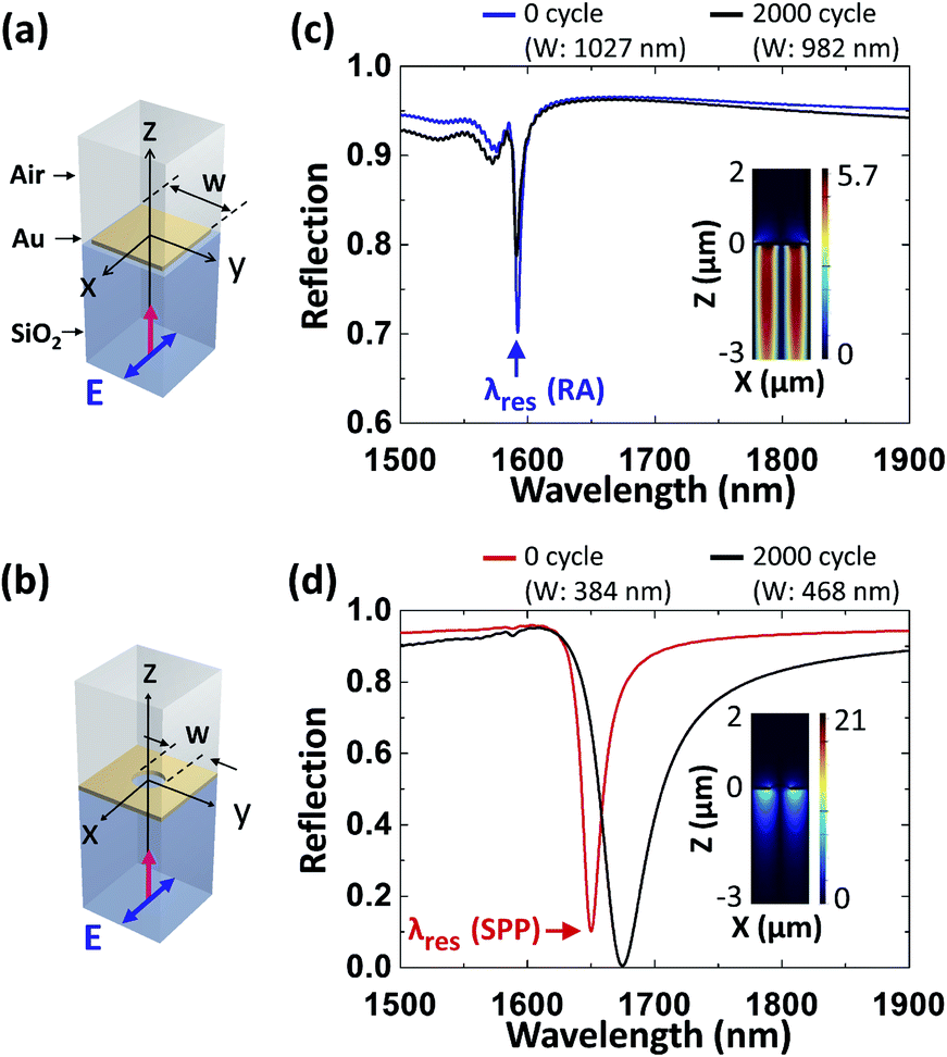 | ||
| Fig. 5 Schematic of 3D unit cell simulation models for (a) square Au nanopatch array and (b) circular Au nanohole array (P = 1100 nm). Simulated reflection spectra of (c) the square Au nanopatch array and (d) circular Au nanohole array before thermal loading and after 2000 cycles of thermal loading. The insets show the electric field distributions (|Ez| at y = 0) at the λres before thermal loading. | ||
| Thermal loading cycle | W (nm) | λ res (nm) | FWHM (nm) | Extres | |
|---|---|---|---|---|---|
| Square Au nanopatch array | 0 | 1027 | 1592.09 | 5.14 | 0.264 |
| 2000 | 982 | 1591.20 | 6.50 | 0.175 | |
| Change | −45 | −0.89 | 1.36 | −0.089 | |
| Circular Au nanohole array | 0 | 384 | 1650.06 | 18.88 | 0.857 |
| 2000 | 468 | 1674.65 | 47.62 | 0.946 | |
| Change | 84 | 24.59 | 28.74 | 0.089 |
2.5 Au nanopatch array on optical fiber
A high duty-cycle square and rectangular Au nanopatch array was fabricated on the end-face of a single-mode optical fiber using focused-ion-beam (FIB) lithography [Fig. 6a]. The square and rectangular nanopatch array forms an on-fiber high-Q plasmonic crystal cavity, as shown in Fig. 6b. The square nanopatch array in the cavity excites SPPs from the incident light, and the surrounding rectangular nanopatch array, which serves as a distributed Bragg reflector (DBR), confines the excited SPPs in the cavity. Details on the operation principle of the on-fiber plasmonic crystal cavity and its application for SPR sensing were reported previously.33,35,36 The periodicities of the fabricated Au nanopatch array are 1030 nm for the cavity, 525 nm for the DBR, and 900 nm for the separation between the cavity and DBR, respectively, and the gap size is 70 nm for all the regions [Fig. 6b and d].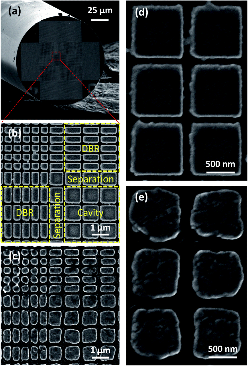 | ||
| Fig. 6 SEM images of the fabricated Au nanopatch array on a single-mode optical fiber: (a) the fiber end-face with a plasmonic crystal cavity, a corner section of the plasmonic cavity (b) before thermal loading and (c) after 500 cycles of thermal loading, and the square Au nanopatches in the plasmonic cavity (d) before thermal loading and (e) after 500 cycles of thermal loading. | ||
The fabricated on-fiber Au nanopatch array was exposed to cyclic thermal loading in the temperature range from 25 °C to 500 °C. The cyclic thermal loading induced similar changes in the pattern geometry and surface morphology of the on-fiber Au nanopatch array as those observed in the on-substrate Au nanostructures. Specifically, the corners and edges of the patches became blunt and patch sizes decreased, resulting in increased gap sizes (i.e., decreased pattern sizes) [Fig. 6c and e]. As large patches suffered from more deformations than small patches, the gap size from large patches increased even more. The measured gap sizes are shown in Table 2. Furthermore, large Au lumps were developed on the surface of the nanopatch arrays [Fig. 6e].
| Gap location | Gap size (nm) | |
|---|---|---|
| Before thermal loading | All domain | 71 ± 13 |
| After thermal loading (500 cycles) | Cavity | 179 ± 24 |
| Between cavity and separation | 148 ± 30 | |
| Between separation and DBR | 112 ± 11 | |
| DBR | 98 ± 11 |
The SPR reflection spectra obtained from the on-fiber Au nanopatch array changed dramatically under cyclic thermal loading, as shown in Fig. 7a. Before thermal loading the narrow-linewidth SPR was located at 1552 nm. The cyclic thermal loading induced a decrease in the resonance slope (Sres), a blueshift in λres, and a decrease in Extres [Fig. 7b and c]. These changes are mainly attributed to the thermal deformation of the Au nanopatch array. In other words, the thermal deformation decreases the duty-cycle of the Au nanopatch array, which induces a blueshift in the Bragg wavelength of the DBRs and thus the resonance wavelength. To verify the influence of the thermal deformation, 2D FDTD simulations were carried out for different geometries of on-fiber 1D Au nanopatch arrays based on the values in Table 2. According to the simulation results [Fig. 7d], the geometry change (i.e., increase in the gap size) could induce the observed SPR profile evolutions. However, the simulated spectra did not capture the complete collapse of the left shoulder of the SPR after 500 cycles of thermal loading. This discrepancy is believed to be due to the non-uniform geometry and surface roughness of the thermally deformed nanopatches. Interestingly, the experimental results showed increases in Extres and Sres after the first 40 cycles of thermal loading and the performance degradation only happened after a larger number of thermal loadings. This early-cycle SPR enhancement is believed to due to Ti layer diffusion. A previous study showed that a Ti adhesion layer used for lithographic planar Au nanorods could diffuse away during a high-temperature annealing process and the corresponding decrease in the damping caused by Ti could enhance the LSPR of Au nanorods.9 Note that the on-fiber nanopatch array deformed more than the on-substrate nanopatch array after thermal loading. This could be attributed to the edge profile difference between the FIB and e-beam fabricated samples and the gallium ion doping during FIB milling. Furthermore, larger CTE (α) mismatch of the on-fiber sample (αAu = 14.2 × 10⁻⁶/°C, αSiO2 (fiber) = 0.5 × 10⁻⁶/°C, αSi = 2.6 × 10⁻⁶/°C) could cause more deformation.
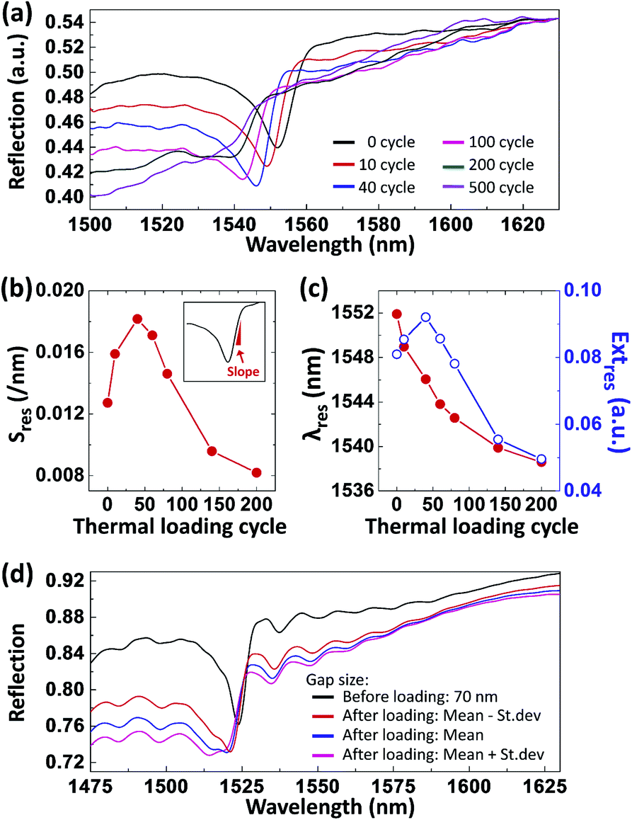 | ||
| Fig. 7 Optical characteristics of the on-fiber Au nanopatch array in experiments: (a) reflection spectra measured at room temperature before thermal loading and after 10, 40, 100, 200, and 500 cycles of thermal loading, (b) measured Sres, (c) λres, and Extres as a function of thermal loading cycle. (d) Simulated reflection spectra before and after 500 thermal loading cycles. Before loading, the designed gap size of 70 nm was used. After loading, the three different spectra were obtained with the measured mean gap sizes, mean − standard deviation, and mean + standard deviation. | ||
For the potential application of the on-fiber Au nanopatch array in refractive index sensing, the influence of the thermal deformation on the sensing performances was analyzed with 2D FDTD simulations. Fig. 8a and b show the simulated reflection spectra of the on-fiber Au nanopatch array before and after thermal loading, respectively, with changes in the refractive index (Δn) of the optical fiber. Note that Δn was applied to the optical fiber since the resonance modes are distributed in the optical fiber. The gap sizes of the Au nanopatch array before and after thermal loading were modeled to be 70 nm and the mean values in Table 2, respectively. For both simulation models, the λres redshifts with increasing Δn, as shown in Fig. 8c. However, the Au nanopatch array after thermal loading has a 0.7% lower λres sensitivity (1034 nm per RIU) than that of the Au nanopatch array before thermal loading (1041 nm per RIU). Such a decrease in the λres sensitivity is attributed to the reduced duty-cycle of the Au nanopatch array due to the thermal deformation. As for the intensity-modulated sensing with a probe laser wavelength located at the FWHM points (1526.31 nm and 1523.76 nm for the Au nanopatch array before and after thermal loading, respectively), the Au nanopatch array after thermal loading has a 35.3% lower reflection sensitivity than that of the Au nanopatch array before thermal loading [Fig. 8d], which results from the lower slope of the resonance.
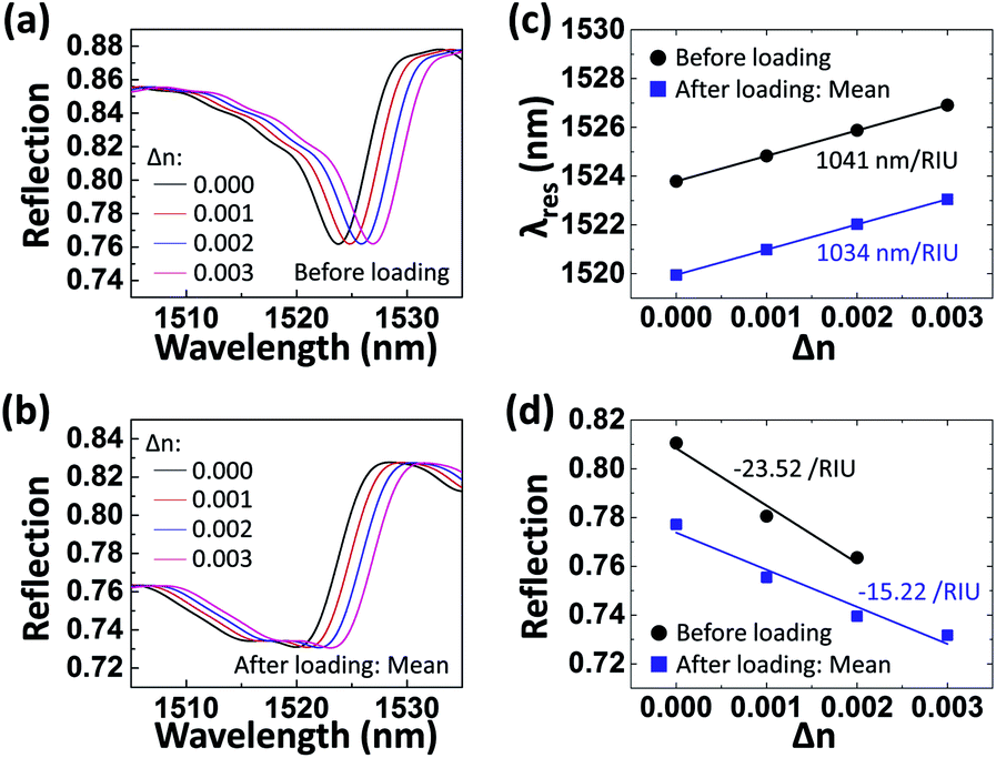 | ||
| Fig. 8 Simulated reflection spectra of the on-fiber Au nanopatch array (a) before and (b) after thermal loading with respect to the changes in the refractive index of the optical fiber. (c) Simulated λres shifts as a function of the refractive index change. (d) Simulated reflections at the 1526.31 nm and 1523.76 nm of wavelengths for the Au nanopatch array before and after thermal loading, respectively, as a function of the refractive index change. | ||
3. Conclusion
We investigated deformation of lithographic planar Au nanopatch and nanohole arrays under cyclic thermal loading and its influence to SPR sensing. The cyclic thermal loading induced changes in the pattern geometry and surface morphology of the Au nanostructures on a Si substrate. The pattern geometry changes include blunting of the pattern boundary (e.g., corners and edges) and decreasing (and increasing) of the nanopatch (and nanohole) size. The surface morphology change includes formation of large Au lumps Furthermore, the pattern area changes (ΔA/A0) obtained from cyclic thermal loading experiments and simulated thermal stresses of different shapes and sizes of Au nanostructures were analyzed to understand the influence of the pattern geometry on the degree and mechanism of the thermal deformation. From the comparison between the experimental results and simulated thermal stresses, capillarity is believed to govern the deformation of the Au nanopatch arrays and ΔA/A0 is independent of gap sizes of the adjacent patterns, while the thermal stress is believed to dominate the deformation of the Au nanohole arrays and ΔA/A0 increases with increased gap sizes.Based on the measured ΔA, the influence of the thermal deformation on SPR sensing were analyzed for two Au nanostructures: a square Au nanopatch array for RA-based sensing and a circular Au nanohole array for SPP-based sensing. The simulated reflection spectra showed that the thermal deformation affects the SPR sensing performance in terms of resonance wavelength (λres), full-width half-maximum (FWHM) of the resonance, and extinction of the reflection at the λres in both cases. However, the square nanopatch array seemed to be more robust to the thermal deformation than the circular nanohole array, which could make it a better choice for elevated temperature applications.
Finally, for the Au nanopatch array on the optical fiber end-face, thermal loading induced similar changes in the pattern geometry and surface morphology as observed in the on-substrate Au nanostructures. Changes in the λres, Extres, and Sres were characterized after various number of thermal loading cycles. Moreover, the performance changes in the refractive index sensing before and after thermal loading were investigated with simulation studies.
We believe that the achieved understanding of thermal deformation of the Au nanostructures and its influence to SPR sensing will provide guidance for the development of robust high-performance plasmonic sensors for monitoring various parameters in elevated temperature environments. This work is also expected to provide useful insights into the thermal deformation of refractory plasmonic nanostructures that can be used at extreme temperature.
4. Experimental section
4.1 Fabrication of Au nanostructures
For the Si substrate sample, a 1 μm of SiO2 film was grown on a Si substrate through thermal oxidation. The SiO2/Si substrate was spin-coated with poly(methyl methacrylate) (PMMA A4, MicroChem) and was patterned using e-beam lithography (e-line, Raith). Then, a 3 nm/60 nm of Ti/Au film was deposited on the substrate using e-beam evaporation (Denton Vacuum Explorer 14, Denton Vacuum). Here, the Ti was used to enhance the adhesion between the Au and SiO2 films. Lastly, the Ti/Au film on the poly(methyl methacrylate) was lifted-off in a solvent stripper (Remover PG, MicroChem). The thickness of the Ti/Au film was measured to be approximately 68 nm using a profilometer (Alpha step 200, Tencor). For the optical fiber sample, a single-mode optical fiber (SMF-28, Corning) was cleaved, so that the fiber end-face was perpendicular to the waveguide direction. The fiber end-face was cleaned by acetone, isopropyl alcohol, and deionized water followed by nitrogen blow. A 3 nm/60 nm of Ti/Au film was deposited on the fiber end-face using e-beam evaporation. The Ti/Au film on the fiber end-face was patterned to the square and rectangular nanopatch array using FIB lithography (GAIA3, Tescan). Note that the Ti/Au films for both optical fiber sample and Si substrate sample were deposited in the same chamber at the same time.4.2 Cyclic thermal loading
Cyclic thermal loading for the Si substrate and optical fiber samples was carried out using furnaces. A tube-type furnace (Lindberg, Thermo Scientific) was used for the Si substrate sample, and a portable table-top furnace (Pro-L, RapidFire) was used for the optical fiber sample. Both Si and optical fiber samples were kept in the furnace (500 °C) and room temperature air (25 °C) for 30 s, respectively, and the transition between the furnace and room temperature air took place for 30 s. It should be noted that the 30 s exposure to 500 °C induces a thermal stress but may not lead to the temperature instability of the Au nanostructures.4.3 Imaging of Au nanostructures and image processing
The low-resolution SEM images in Fig. 1, 2a–c and S1† were acquired using a variable pressure SEM (S-3400, Hitachi) without additional metal coating. On the other hand, the high-resolution SEM images in Fig. 2d, e, 3 and 6 were acquired with sputtering of thin-film Au (less than 10 nm) to the samples before SEM imaging (XEIA, Tescan). The acquired SEM images were processed with OpenCV functions to measure the pattern area as follows. First, the SEM images were converted into grayscale images (cv2.Color_BGR2GRAY). Then, the contrast of the grayscale images was improved through histogram equalization (cv2.equalizeHist), which helped clarify the pattern boundary. Further, Gaussian blurring was applied to the processed images to reduce noise in the images (cv2.GaussianBlur). The blurred images were then binarized with a predefined threshold (cv2.THRESH_OTSU). Next, the area of patterns was calculated in a pixel scale using a contour function (cv2.contourArea). Finally, the area in the pixel scale was converted into a μm scale based on the scale bar in the original SEM image.4.4 Thermal-mechanical simulations
Thermal stress on the Au nanostructures was calculated with FEM simulations (COMSOL Multiphysics). The Au nanostructures were modeled with a 3D unit cell with periodic boundary conditions. The reference temperature and temperature for stress analysis were set to 25 °C and 500 °C, respectively. von-Mises stresses on the top surface of the Au nanostructures were calculated using the solid mechanics module with the linear elastic material model, and the material properties of Au, SiO2, and Si were adapted from the material library of the software. Note the calculated stresses may be different from the actual stresses since simulations do not account for the plastic deformation. However, they can provide useful insights into the thermal stress profiles among different shapes and sizes of Au nanostructures.4.5 Optical simulations
FDTD software (Lumerical FDTD Solutions) was used for the optical simulations. For the 3D simulations of the unit cells of the square nanopatch and circular nanohole arrays (Fig. 5), the Bloch boundary condition was used for the x and y boundaries and the perfectly matched layer (PML) condition was used for the z boundaries. A plane wave with linear polarization was used as incident light. For the 2D FDTD simulations of the on-fiber 1D Au nanopatch array (Fig. 7d and 8), the fiber core and cladding were modeled with 9 μm and 125 μm of diameters, respectively. The cavity was modeled with 14 arrays of nanopatches (P = 1030 nm) and the surrounding DBRs were modeled with 80 arrays of nanopatches (P = 525 nm). The PML condition was used for all the boundaries. A fiber guided mode was used for incident light. For both simulation models the refractive index of Au was adapted from the materials database of the FDTD software,37 and the refractive indices of the core and cladding were 1.450 and 1.445, respectively. The ambient refractive index was 1.000.4.6 Characterization of on-fiber Au nanopatch array
The reflection spectra of the on-fiber Au nanopatch array were obtained by using a tunable laser (TSL-510, Santec), a 2 × 1 coupler, a polarization controller (FPC030, Thorlabs), and a photodetector (2011-FC, New Focus). Light from the tunable laser was coupled into the Au nanopatch array on the fiber end-face through the 2 × 1 coupler. The incident light was linearly polarized to either direction of the array using the polarization controller. The reflected light from the fiber end-face was monitored with the photodetector.Authors contributions
H.-T. K. designed the experiments, performed nanofabrication, took SEM images, carried out FEM and FDTD simulations, and analyzed the experimental and simulation data. M. P. processed the SEM images and carried out the cyclic thermal loading experiments for the optical fiber sample. K. R. carried out the cyclic thermal loading experiments for the Si substrate sample. H.-T. K. and M. Y. wrote the manuscript. M. Y. and A. K. G supervised the project.Conflicts of interest
There are no conflicts to declare.Acknowledgements
This work was supported by Office of Naval Research High-Temperature Energy Systems (HiTES) program and National Science Foundation.Notes and references
- C. J. Murphy, T. K. Sau, A. M. Gole, C. J. Orendorff, J. Gao, L. Gou, S. E. Hunyadi and T. Li, J. Phys. Chem. B, 2005, 109, 13857–13870 CrossRef CAS PubMed
.
- N. Halas, MRS Bull., 2005, 30, 362–367 CrossRef CAS
- Y.-Y. Yu, S.-S. Chang, C.-L. Lee and C. C. Wang, J. Phys. Chem. B, 1997, 101, 6661–6664 CrossRef CAS
- V. R. Shrestha, S.-S. Lee, E.-S. Kim and D.-Y. Choi, Nano Lett., 2014, 14, 6672–6678 CrossRef CAS PubMed
- T. W. Ebbesen, H. J. Lezec, H. Ghaemi, T. Thio and P. A. Wolff, Nature, 1998, 391, 667 CrossRef CAS
- S. H. Lee, K. C. Bantz, N. C. Lindquist, S.-H. Oh and C. L. Haynes, Langmuir, 2009, 25, 13685–13693 CrossRef CAS PubMed
- C. L. Haynes and R. P. Van Duyne, J. Phys. Chem. B, 2001, 105, 5599–5611 CrossRef CAS
- P. R. Ohodnicki, M. P. Buric, T. D. Brown, C. Matranga, C. Wang, J. Baltrus and M. Andio, Nanoscale, 2013, 5, 9030–9039 RSC
- N. A. Joy, B. K. Janiszewski, S. Novak, T. W. Johnson, S.-H. Oh, A. Raghunathan, J. Hartley and M. A. Carpenter, J. Phys. Chem. C, 2013, 117, 11718–11724 CrossRef CAS
- N. Karker, G. Dharmalingam and M. A. Carpenter, ACS Nano, 2014, 8, 10953–10962 CrossRef CAS PubMed
- G. Baffou, R. Quidant and C. Girard, Appl. Phys. Lett., 2009, 94, 153109 CrossRef
- G. Baffou and R. Quidant, Laser Photonics Rev., 2013, 7, 171–187 CrossRef CAS
- W. Challener, C. Peng, A. Itagi, D. Karns, W. Peng, Y. Peng, X. Yang, X. Zhu, N. Gokemeijer and Y.-T. Hsia, Nat. Photonics, 2009, 3, 220 CrossRef CAS
- C. Wu, B. Neuner III, J. John, A. Milder, B. Zollars, S. Savoy and G. Shvets, J. Opt., 2012, 14, 024005 CrossRef
- L. R. Hirsch, R. J. Stafford, J. Bankson, S. R. Sershen, B. Rivera, R. Price, J. D. Hazle, N. J. Halas and J. L. West, Proc. Natl. Acad. Sci. U. S. A., 2003, 100, 13549–13554 CrossRef CAS PubMed
- H. Reddy, U. Guler, A. V. Kildishev, A. Boltasseva and V. M. Shalaev, Opt. Mater. Express, 2016, 6, 2776–2802 CrossRef CAS
- H. Reddy, U. Guler, Z. Kudyshev, A. V. Kildishev, V. M. Shalaev and A. Boltasseva, ACS Photonics, 2017, 4, 1413–1420 CrossRef CAS
- H. Reddy, U. Guler, K. Chaudhuri, A. Dutta, A. V. Kildishev, V. M. Shalaev and A. Boltasseva, ACS Photonics, 2017, 4, 1083–1091 CrossRef CAS
- K. M. Mayer and J. H. Hafner, Chem. Rev., 2011, 111, 3828–3857 CrossRef CAS PubMed
- J. Steele, C. Moran, A. Lee, C. Aguirre and N. Halas, Phys. Rev. B: Condens. Matter Mater. Phys., 2003, 68, 205103 CrossRef
- A. B. Taylor, A. M. Siddiquee and J. W. Chon, ACS Nano, 2014, 8, 12071–12079 CrossRef CAS PubMed
- Y. Wang, S. Teitel and C. Dellago, Nano Lett., 2005, 5, 2174–2178 CrossRef CAS PubMed
- H. Petrova, J. P. Juste, I. Pastoriza-Santos, G. V. Hartland, L. M. Liz-Marzán and P. Mulvaney, Phys. Chem. Chem. Phys., 2006, 8, 814–821 RSC
- Y. Liu, E. N. Mills and R. J. Composto, J. Mater. Chem., 2009, 19, 2704–2709 RSC
- W. Li, U. Guler, N. Kinsey, G. V. Naik, A. Boltasseva, J. Guan, V. M. Shalaev and A. V. Kildishev, Adv. Mater., 2014, 26, 7959–7965 CrossRef CAS PubMed
- Y. Khalavka, C. Ohm, L. Sun, F. Banhart and C. Sönnichsen, J. Phys. Chem. C, 2007, 111, 12886–12889 CrossRef CAS
- Y.-S. Chen, W. Frey, S. Kim, K. Homan, P. Kruizinga, K. Sokolov and S. Emelianov, Opt. Express, 2010, 18, 8867–8878 CrossRef CAS PubMed
- W. Mullins, Metall. Mater. Trans. A, 1995, 26, 1917–1929 CrossRef
-
G. Zhang and Z. Wang, in Multiscale fatigue crack initiation and propagation of engineering materials: structural integrity and microstructural worthiness, Springer, 2008, pp. 275–326 Search PubMed
- S. Kumar, X. Li, A. Haque and H. Gao, Nano Lett., 2011, 11, 2510–2516 CrossRef CAS PubMed
- F. Nichols and W. Mullins, J. Appl. Phys., 1965, 36, 1826–1835 CrossRef
- S. Ri, T. Sugano, M. Saka, M. Yamashita and F. Togoh, Strength, Fracture and Complexity, 2011, 7, 61–70 Search PubMed
- H.-T. Kim and M. Yu, Sci. Rep, 2019, 9, 1922 CrossRef PubMed
- Z. Zhang, Y. Chen, H. Liu, H. Bae, D. A. Olson, A. K. Gupta and M. Yu, Opt. Express, 2015, 23, 10732–10740 CrossRef CAS PubMed
- X. He, H. Yi, J. Long, X. Zhou, J. Yang and T. Yang, Appl. Phys. Lett., 2016, 108, 231105 CrossRef
- X. Zhou, D. Cai, X. He, S.-L. Chen, X. Wang and T. Yang, Opt. Lett., 2018, 43, 775–778 CrossRef CAS PubMed
-
G. Ghosh and E. D. Palik, Handbook of Optical Constants of Solids, Five-Volume Set: Handbook of Thermo-Optic Coefficients of Optical Materials with Applications, Elsevier Science, 1997 Search PubMed
Footnote |
| † Electronic supplementary information (ESI) available. See DOI: 10.1039/c9na00714h |
| This journal is © The Royal Society of Chemistry 2020 |