
Tungsten oxide nanostructures and nanocomposites for photoelectrochemical water splitting
Guangwei
Zheng
ab,
Jinshu
Wang
 *a,
Hu
Liu
*c,
Vignesh
Murugadoss
bd,
Guannan
Zu
a,
Haibing
Che
a,
Chen
Lai
a,
Hongyi
Li
a,
Tao
Ding
*e,
Qiang
Gao
*f and
Zhanhu
Guo
*b
*a,
Hu
Liu
*c,
Vignesh
Murugadoss
bd,
Guannan
Zu
a,
Haibing
Che
a,
Chen
Lai
a,
Hongyi
Li
a,
Tao
Ding
*e,
Qiang
Gao
*f and
Zhanhu
Guo
*b
aKey Lab of Advanced Functional Materials, Ministry of Education, College of Materials Science and Engineering, Beijing University of Technology, Beijing 100124, China. E-mail: wangjsh@bjut.edu.cn
bIntegrated Composites Laboratory (ICL), Department of Chemical & Biomolecular Engineering, University of Tennessee, Knoxville, TN 37996, USA. E-mail: zguo10@utk.edu
cKey Laboratory of Materials Processing and Mold (Zhengzhou University), Ministry of Education, National Engineering Research Center for Advanced Polymer Processing Technology, Zhengzhou University, Zhengzhou, 450002, Henan, China. E-mail: liuhu@zzu.edu.cn
dPondicherry University, Centre for Nanoscience and Technology, Puducherry, 605014, India
eCollege of Chemistry and Chemical Engineering, Henan University, Kaifeng, 475004, Henan, China. E-mail: dingtao@henu.edu.cn
fScanning Probe Microscopy Group, Center for Nanophase Materials Sciences, Oak Ridge National Laboratory, P.O. Box 2008, Oak Ridge, TN 37831, USA. E-mail: gaoq@ornl.gov
First published on 28th June 2019
Abstract
Hydrogen production from photoelectrochemical (PEC) water splitting using semiconductor photocatalysts has attracted great attention to realize clean and renewable energy from solar energy. The visible light response of WO3 with a long hole diffusion length (∼150 nm) and good electron mobility (∼12 cm2 V−1 s−1) makes it suitable as the photoanode. However, WO3 suffers from issues including rapid recombination of photoexcited electron–hole pairs, photo-corrosion during the photocatalytic process due to the formation of peroxo-species, sluggish kinetics of photogenerated holes, and slow charge transfer at the semiconductor/electrolyte interface. This work highlights the approaches to overcome these drawbacks of WO3 photoanodes, including: (i) the manipulation of nanostructured WO3 photoanodes to decrease the nanoparticle size to promote hole migration to the WO3/electrolyte interface which benefits the charge separation; (ii) doping or introducing oxygen vacancies to improve electrical conductivity; exposing high energy crystal surfaces to promote the consumption of photogenerated holes on the high-active crystal face, thereby suppressing the recombination of photogenerated electrons and holes; (iii) decorating with co-catalysts to reduce the overpotential which inhibits the formation of peroxo-species; (iv) other methods such as coupling with narrow band semiconductors to accelerate the charge separation and controlling the crystal phase via annealing to reduce defects. These approaches are reviewed with detailed examples.
1. Introduction
The scarcity and growing demands of fossil fuels require our society to develop efficient, clean and renewable energy.1–4 Photocatalytic water splitting to produce H2 has become an effective approach to address these issues.5,6 Since the pioneering studies by Becquerel in 1839![[thin space (1/6-em)]](https://www.rsc.org/images/entities/char_2009.gif) 7 and Fujishima and Honda in 1972,8 photocatalytic and photoelectrochemical (PEC) water splitting using semiconductors under solar irradiation have attracted remarkable attention. Afterwards, various photocatalysts including hematite,9 BiVO4,10–12 WO3,13–15 TiO2,16,17 ZnO,18 CdS,19 TaON,20 IrO2,21 SrTiO3,22,23 Ta3N5,24 and BiFeO325 have been exploited as photoanodes. Metal chalcogenides, e.g., CdS and MoS2, have been reported as promising photocatalysts for water splitting because of their narrow band gap,26 while they are more susceptible to degradation during the water oxidation reaction. Oxides are the most photochemically stable semiconductors in aqueous solution,27 though TiO2 and ZnO have a wide band gap energy that can be excited only by UV photons. Among the myriad of oxides, WO3 with a band gap of 2.4–2.8 eV (ref. 28) has been considered to be the most promising visible light responsive photoanode for PEC water splitting. The large valence band (VB) of WO3 located at approximately 3.0 V vs. NHE makes it appropriate for water oxidation. WO3 possesses a moderate hole diffusion length (∼150 nm) compared with α-Fe2O3 (2–4 nm) and better electron mobility (∼12 cm2 V−1 s−1) compared to TiO2 (∼0.3 cm2 V−1 s−1).29 Moreover, the low-cost WO3 exhibits excellent stability and the carriers move quickly under solar irradiation.30,31 Nevertheless, the activity of WO3 for PEC water splitting still needs to be improved. As an indirect semiconductor, WO3 requires a relatively thick film for adequate light absorption which causes a significant recombination of electrons and holes, and thus decreases the performance of PEC water splitting.32 During water splitting, the possibly formed peroxo-species on the WO3 surface accelerate the photo-corrosion and consequently reduce the stability of the WO3 photoanode.32,33 The sluggish kinetics of photogenerated holes and charge transfer at the semiconductor/electrolyte interface intensify the drawback of the WO3 photoanode.29,34,35 The maximum theoretical solar-to-hydrogen efficiency of WO3 is ∼6% and the theoretical photocurrent density is 4 mA cm−2 under Air Mass 1.5 Global (AM 1.5 G) solar illumination. The WO3-based PEC devices cannot compete directly with coupled solar and electrolysis with an efficiency of about 10%. Nevertheless, modified WO3-based PEC can potentially achieve efficiencies beyond 10% at a low cost.36 Considerable attempts have been made to solve the issues including doping, orderly nanostructured morphologies, coupling with narrow band semiconductors, introducing oxygen vacancies, decorating with co-catalysts, etc.
7 and Fujishima and Honda in 1972,8 photocatalytic and photoelectrochemical (PEC) water splitting using semiconductors under solar irradiation have attracted remarkable attention. Afterwards, various photocatalysts including hematite,9 BiVO4,10–12 WO3,13–15 TiO2,16,17 ZnO,18 CdS,19 TaON,20 IrO2,21 SrTiO3,22,23 Ta3N5,24 and BiFeO325 have been exploited as photoanodes. Metal chalcogenides, e.g., CdS and MoS2, have been reported as promising photocatalysts for water splitting because of their narrow band gap,26 while they are more susceptible to degradation during the water oxidation reaction. Oxides are the most photochemically stable semiconductors in aqueous solution,27 though TiO2 and ZnO have a wide band gap energy that can be excited only by UV photons. Among the myriad of oxides, WO3 with a band gap of 2.4–2.8 eV (ref. 28) has been considered to be the most promising visible light responsive photoanode for PEC water splitting. The large valence band (VB) of WO3 located at approximately 3.0 V vs. NHE makes it appropriate for water oxidation. WO3 possesses a moderate hole diffusion length (∼150 nm) compared with α-Fe2O3 (2–4 nm) and better electron mobility (∼12 cm2 V−1 s−1) compared to TiO2 (∼0.3 cm2 V−1 s−1).29 Moreover, the low-cost WO3 exhibits excellent stability and the carriers move quickly under solar irradiation.30,31 Nevertheless, the activity of WO3 for PEC water splitting still needs to be improved. As an indirect semiconductor, WO3 requires a relatively thick film for adequate light absorption which causes a significant recombination of electrons and holes, and thus decreases the performance of PEC water splitting.32 During water splitting, the possibly formed peroxo-species on the WO3 surface accelerate the photo-corrosion and consequently reduce the stability of the WO3 photoanode.32,33 The sluggish kinetics of photogenerated holes and charge transfer at the semiconductor/electrolyte interface intensify the drawback of the WO3 photoanode.29,34,35 The maximum theoretical solar-to-hydrogen efficiency of WO3 is ∼6% and the theoretical photocurrent density is 4 mA cm−2 under Air Mass 1.5 Global (AM 1.5 G) solar illumination. The WO3-based PEC devices cannot compete directly with coupled solar and electrolysis with an efficiency of about 10%. Nevertheless, modified WO3-based PEC can potentially achieve efficiencies beyond 10% at a low cost.36 Considerable attempts have been made to solve the issues including doping, orderly nanostructured morphologies, coupling with narrow band semiconductors, introducing oxygen vacancies, decorating with co-catalysts, etc.
Previous reviews have been presented the use of WO3 in gas sensors, electrochromic, photochromic, and photocatalytic degradation. However, the strategies to improve the performance of WO3 photoanodes for PEC water splitting have been rarely summarized. In this review, recent progress in the WO3 photoanodes and the possibility of using WO3 for direct Z-scheme overall water splitting are documented with detailed examples. The strategies to overcome the limitations of WO3 as the photoanode are summarized to enhance the photocatalytic activity for PEC water splitting with detailed examples. (1) The PEC water splitting performance of WO3 suffers from the recombination of electron–hole pairs. WO3 nanostructures with small sizes and controllable morphologies can decrease the diffusion length of holes and reduce the grain boundaries to benefit the charge separation.37 Doping with a hetero-element or introducing oxygen vacancies can improve electrical conductivity and facilitate charge transfer.38 Moreover, exposing high energy crystal surfaces can promote the consumption of photoexcited holes on the high-active crystal face, which reduces the recombination of photogenerated electron–hole pairs.32 Coupling with a narrow band gap semiconductor can form an internal electric field at the interface which facilitates the separation of photogenerated electrons and holes and restricts the recombination.39 (2) During the oxygen evolution reaction (OER), peroxo species formed and accumulated on the surface of WO3 become kinetically competitive with O2 production, and thus result in photo-corrosion. Decorating with co-catalysts can improve the surface kinetics and reduce the OER overpotential that inhibits the formation of peroxo species.40 The optimized crystallinity and exposing highly active crystal surface can impede the formation of peroxo species on the surface of WO3.41 (3) Although coupling with a narrower band gap semiconductor to form type II heterojunctions can improve the PEC water splitting performance, it is limited to realize overall water splitting without changing the original oxidation and reduction potential. To achieve overall water splitting efficiency, coupling with a narrow bandgap semiconductor to create a direct Z-scheme system can significantly promote an efficient charge separation as well as maintain the optimized redox ability.
2. Photocatalytic and PEC water splitting mechanism
The fundamental principle of one-step overall water splitting on a semiconductor is shown in Fig. 1a. Under light irradiation with an energy no less than the band gap of a semiconductor, electrons excited from the VB move to the conduction band (CB), leaving holes in the VB.42 Under standard conditions, the overall water splitting is an uphill reaction requiring a Gibbs free energy of ΔG = +237.2 kJ mol−1 corresponding to the electrolysis cell voltage of ΔE° = 1.23 V per electron transferred according to the Nernst equation.43 To split the water into H2 and O2, the band-gap energy of the semiconductors should be larger than 1.23 eV. In other words, the CB of the semiconductor should be more negative than 0 V vs. NHE, while the VB of the semiconductor has to be more positive than 1.23 V vs. NHE.44,45 The band gap of the semiconductor should be narrower than 3 eV to achieve visible-light-response sufficiently.46 The semiconductor must be stable in the photocatalytic reaction. At least, the photogenerated carrier transfer from the surface of the semiconductor to the solution must be facile enough to reduce energy loss arising from the kinetic overpotential.47 In this regard, only a few semiconductors are suitable for one-step water splitting.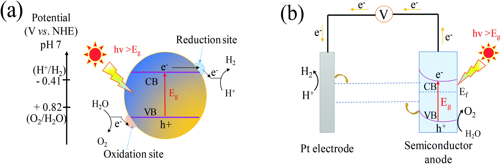 | ||
| Fig. 1 Schematic illustration of (a) photocatalytic water splitting for a one-step photoexcitation system, (b) the basic principles of water splitting for a PEC cell with an n-type semiconductor photoanode and Pt cathode. CB, conduction band; VB, valence band; Eg, band gap; Ef, Fermi level. | ||
PEC is another approach to achieve overall water splitting in which a semiconductor is employed as the photoanode and Pt always as the counter electrode, and both are immersed in an aqueous electrolyte. In this system (Fig. 1b), a bias potential is applied to facilitate the separation of the photoexcited electron–hole pairs due to the formation of a depletion layer in the photoanode. Meanwhile, the applied bias shifts the electrode potential of the metal cathode sufficiently negative of the reversible hydrogen potential and thereby enables the proton reduction.48 It is thus likely for the narrow band gap semiconductor with a CB lower than the energy of H+/H2 to produce hydrogen. Hence many semiconductors were used as photoanodes for the PEC overall water splitting including WO3, despite more positive location of its CB (0.55–0.8 V vs. RHE (reversible hydrogen electrode), pH = 0).49 In the PEC water-splitting cells, hydrogen is produced at the cathode and oxygen evolution takes place at the anode, thus the well physically separated chambers of hydrogen and oxygen can be achieved. This process of PEC water splitting can be summarized by eqn (1) and (2):50
Anodic:
| 2H2O + 4h+ → O2 + 4H+; E° = 1.23 V vs. NHE | (1) |
Cathodic:
| 4H+ + 4e− → 2H2; E° = 0 V vs. NHE | (2) |
The PEC water splitting reaction normally occurs in three steps: (i) the photoanode semiconductor absorbs the photon energy that is higher than the band gap of the semiconductor to excite the electron–hole pairs in the bulk; (ii) the separation of photogenerated charges, i.e., the holes reach the surface of the photoanode to oxidize water molecules into O2 whereas the electrons migrate to the counter electrode to reduce water molecules into H2; (iii) the recombination of photogenerated holes and electrons, inducing a back-electron flow from the external circuit into the photoelectrode.51 The first two steps strongly depend on the structure and electronic properties of the photocatalyst. Concerning the third step, the recombination of holes and electrons restricts the photoconversion efficiency. Therefore, it is significantly necessary to develop a promising visible light response and create highly efficient photocatalysts for the overall water splitting.
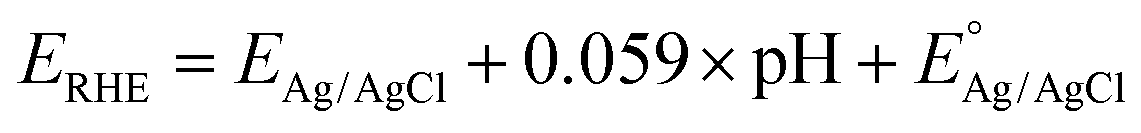
In the PEC water splitting system, the photocurrent density as a function of potential is an important parameter to evaluate its performance. The theoretical photocurrent density of WO3 is reported to be 4 mA cm−2 under AM 1.5 G.32 In a three-electrode system using Ag/AgCl as a reference electrode, the measured electrode potentials vs. Ag/AgCl could be converted to the RHE potential according to the Nernst equation:32,52
 | (3) |
 is 0.197 V at 25 °C.
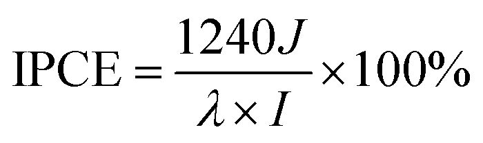
Another important factor for evaluating photoactive behavior is the incident photon-to-current efficiency (IPCE), representing the photocurrent collected per incident photon flux as a function of incident-light wavelength. The IPCE could be calculated at a desired bias voltage from eqn (4):52,53
 | (4) |
3. Strategies to enhance WO3 photocatalytic activity in PEC water system
3.1. Morphological manipulation
Compared with bulk materials, nanostructured materials with a higher specific surface area and more reaction active sites can enhance the photon absorption to improve the photoelectric conversion efficiency.37,54 The size of bulk WO3 is larger than 150 nm, and restricts the hole migration to the surface of WO3. Thanks to a shorter hole transport distance, the nanomaterials could improve the separation efficiency of photogenerated electron–hole pairs and yield a more rapid photoexcited hole injection to the electrolyte. However, small grains can reduce the activity in the visible light region.55 Furthermore, the defects on the crystal surface make it possible for intensive electron–hole recombination which reduces the PEC water splitting performance.34 Thus, developing an appropriate grain size, structure and morphology of the photocatalyst holds the key to improve the photocatalytic performance. The widely used methods for synthesizing WO3 nanostructures include solvothermal,56 hydrothermal,39,57 anodization,58 glancing angle deposition (GLAD),59 pulsed laser deposition (PLD),60 sol–gel,61 chemical vapor deposition (CVD),62 and electrodeposition.40 Meanwhile, the fabrication methods were found to affect the grain boundaries and the dimension of the nanostructures, which limited the efficiency of water splitting. The morphology, fabrication method and PEC water splitting performance of the WO3 photoanode films are illustrated in Table 1. Amongst the myriad of techniques, hydrothermal/solvothermal techniques have been commonly used to synthesize nanostructure WO3 films. During the synthesis, introducing a very thin WO3 dense layer has been found to be a prerequisite for the crystal growth that can hinder the interfacial recombination and decrease the photogenerated electron injection back into the electrolyte on the exposed areas of FTO.59,63 Meanwhile, involving seed layers contributes to form grain boundaries in the nanocrystalline base film which can reduce the photocatalytic activity.64–66| Topography | Fabrication method | Film texture | Photoelectrochemistry | Ref. |
|---|---|---|---|---|
| Nanoplate | 2-Step hydrothermal |
|
Photocurrent: 3.7 mA cm−2 at 1.23 V vs. RHE; IPCE: 67% at 350 nm at 1.23 V vs. RHE; electrolyte: 0.1 M Na2SO4 | 32 |
| Nanoflake | Solvothermal |
|
Photocurrent: ∼1.43 mA cm−2 at 1.23 V vs. RHE; IPCE: ∼70% at 480 nm at 1.23 V vs. RHE; electrolyte: 0.1 M Na2SO4 | 56 |
| Nanorod | Hydrothermal |
|
Photocurrent: 2.26 mA cm−2 at 1.23 V vs. RHE; IPCE: ∼90% at 350 nm at 1.23 V vs. RHE; electrolyte: 0.5 M H2SO4 | 57 |
| Microcrystal | Hydrothermal |
|
Photocurrent: 0.45 mA cm−2 at 0.8 V vs. RHE; IPCE: ∼2.7% at 300 nm at 0.8 V vs. RHE; electrolyte: 1 M H2SO4 | 39 |
| Nanoflake | Anodization |
|
Photocurrent: 0.9 mA cm−2 at 1.2 V vs. RHE; IPCE: ∼42% at 420 nm at 1.2 V vs. RHE; electrolyte: 0.5 M H2SO4 | 58 |
| Nanorod | Glancing angle deposition (GAD) |
|
Photocurrent: 2.15 mA cm−2 at 1.23 V vs. RHE; IPCE: ∼40% at 385 nm at 1.23 V vs. RHE; electrolyte: 0.5 M KPi + 1 M Na2SO3 | 59 |
| Tree-like nanoporous | Pulsed laser deposition (PLD) |
|
Photocurrent: 1.8 mA cm−2 at 1.23 V vs. RHE; IPCE: ∼78% at 350 nm at 1.23 V vs. RHE; electrolyte: 0.5 M KPi + 0.5 M H2SO4 | 60 |
| Nanoplate | Water bath |
|
Photocurrent: ∼1.42 mA cm−2 at 1.23 V vs. RHE; IPCE: ∼38% at 400 nm at 1.23 V vs. RHE; electrolyte: 0.1 M Na2SO4 | 41 |
| Nanoflake | Hydrothermal |
|
Photocurrent: 2.25 mA cm−2 at 1.23 V vs. RHE; IPCE: ∼23.25% at 440 nm at 1.23 V vs. RHE electrolyte: 0.1 M Na2SO4 | 67 |
| Nanoplate | Hydrothermal |
|
Photocurrent: 1.2 mA cm−2 at 1.23 V vs. RHE; IPCE: ∼40% at 350 nm at 1.23 V vs. RHE electrolyte: 1 M H2SO4 | 68 |
| Nanoparticle | Hydrothermal |
|
Photocurrent: 2.7 mA cm−2 at 1.4 V vs. RHE; electrolyte: 0.5 M H2SO4 | 69 |
| Nanoneedle | Pulsed laser deposition (PLD) |
|
Photocurrent: 2.4 mA cm−2 at 1.23 V vs. RHE; IPCE: 50% at 410 nm at 1.23 V vs. RHE; electrolyte: 0.1 M H2SO4 | 70 |
| Nanoflake | Solvothermal |
|
Photocurrent: 1.1 mA cm−2 at 1.23 V vs. RHE; IPCE: ∼45% at 320 nm at 1.23 V vs. RHE; electrolyte: 0.1 M Na2SO4 | 71 |
| Nanoparticle | Polymer-assisted deposition |
|
Photocurrent: 1.45 mA cm−2 at 1.23 V vs. RHE; electrolyte: 0.1 M KPi | 72 |
Note: WO3 is only stable in acidic media of pH lower than 4. That is, the PEC properties of WO3 may be investigated to be unstable in the electrolyte with 4 < pH ≤ 7. Researchers should investigate the PEC performance of WO3 under strong acidic conditions in the future work.
 | ||
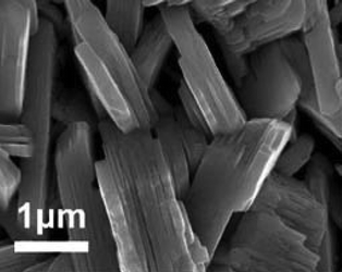
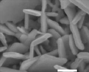
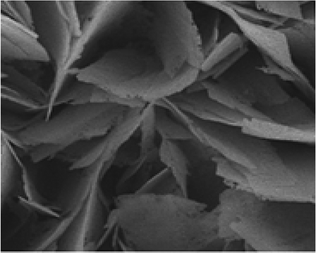
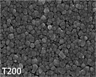
| Fig. 2 FESEM images of (a) unannealed WO3 nanowire, (b) unannealed WO3 nanoflake (NF1) (c) unannealed WO3 nanoflake (NF2), (d) photograph of WO3 films as-prepared and after annealing, (e) current–potential plots for annealed nanowire, and two flake samples, under chopped visible light in an aqueous solution of 0.1 mol L−1 sodium sulfate (Na2SO4), (f) IPCE of three samples with a bias of 0.5 V in a two electrode setup with Pt foil as the counter electrode. Reproduced from ref. 56. Copyright 2011 American Chemical Society. | ||
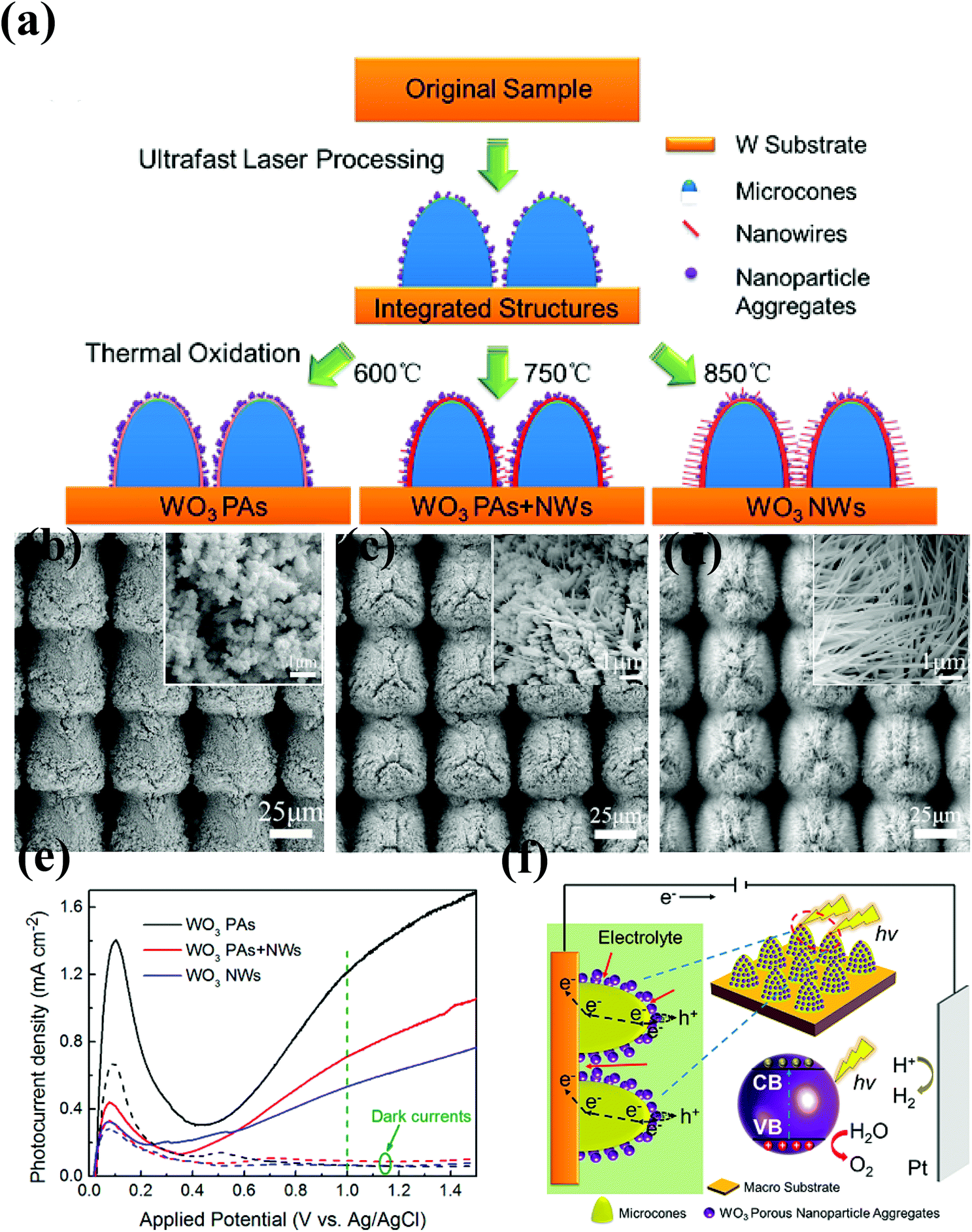 | ||
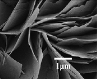
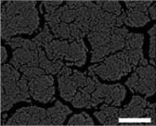
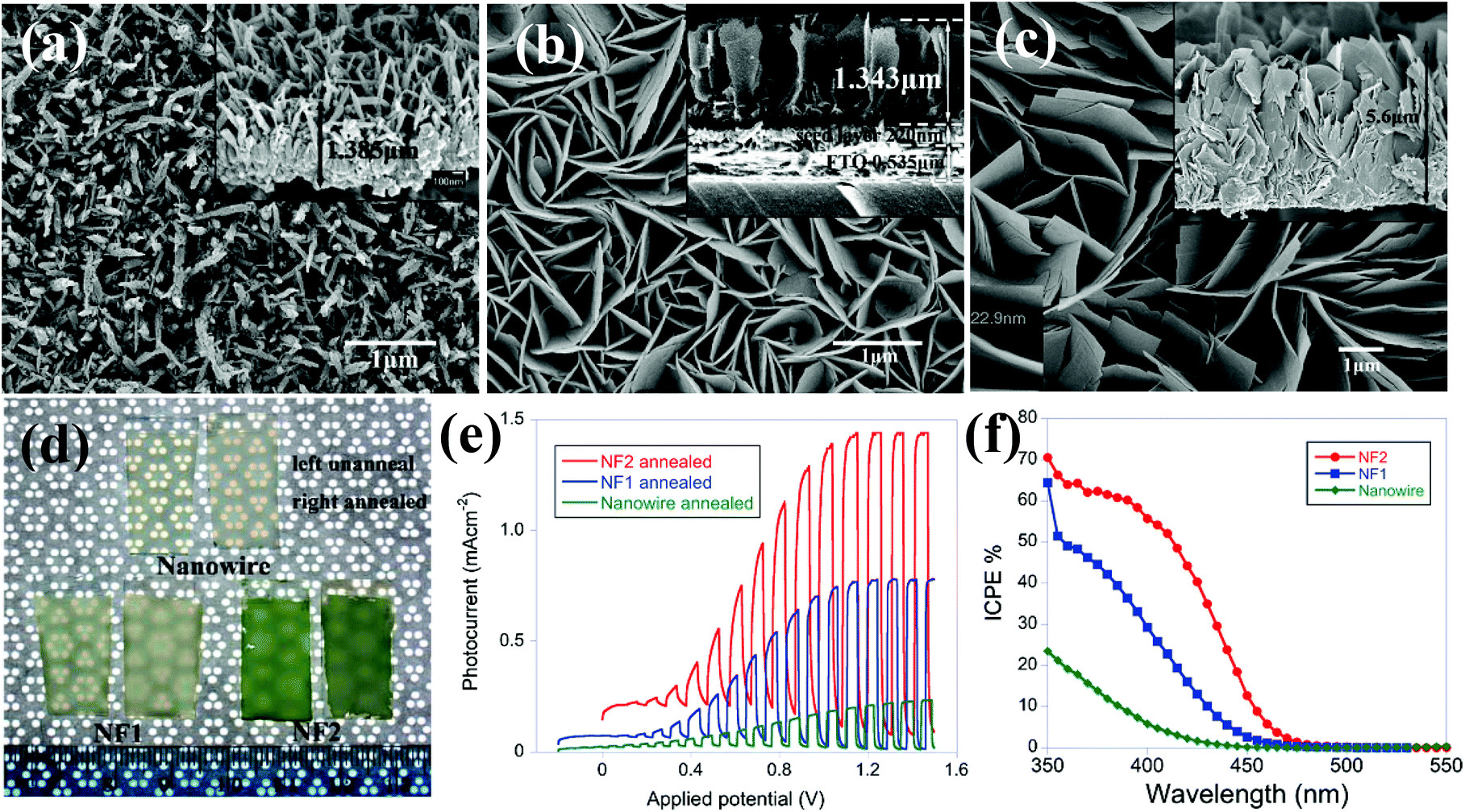
| Fig. 3 (a) Schematic of the strategy of tuning WO3 nanostructures. SEM images of (b) WO3 PAs, (c) WO3 PAs + NWs and (d) WO3 NWs in different magnifications, (e) photocurrent density of three types of WO3 nanostructures vs. potential plots, (f) schematic of the hierarchical structure with porous WO3 nanoparticle aggregates and the corresponding charge transport/transfer and electrolyte permeation processes. The olive color and the arrows represent the electrolyte (0.1 M H2SO4) and the penetration of the electrolyte, respectively. Reproduced from ref. 101. Copyright 2017 American Chemical Society. | ||
3.2. Crystal phase control
An efficient PEC water splitting performance depends on the photoanode; not only on the morphology but also the crystal phase of WO3. The monoclinic phase of WO3 has been demonstrated as the most stable phase at room temperature and its water oxidation activity is stronger than that of the hexagonal phase or orthorhombic phase WO3.29,41,57,77,102–104 With increasing annealed temperatures, WO3·0.33H2O synthesized from the precursor changed from orthorhombic to anhydrous hexagonal and then to stable monoclinic (Fig. 4c). As the heating temperature increased from 400 to 500 °C, the absorption edge showed a continuous red shift and the film turned from greyish to yellow (Fig. 4a). The orthorhombic WO3·0.33H2O demonstrated the lowest photocurrent density, while the monoclinic WO3 annealed at 500 °C exhibited an optimal PEC performance (Fig. 4b).29,41,57,64,65,77,82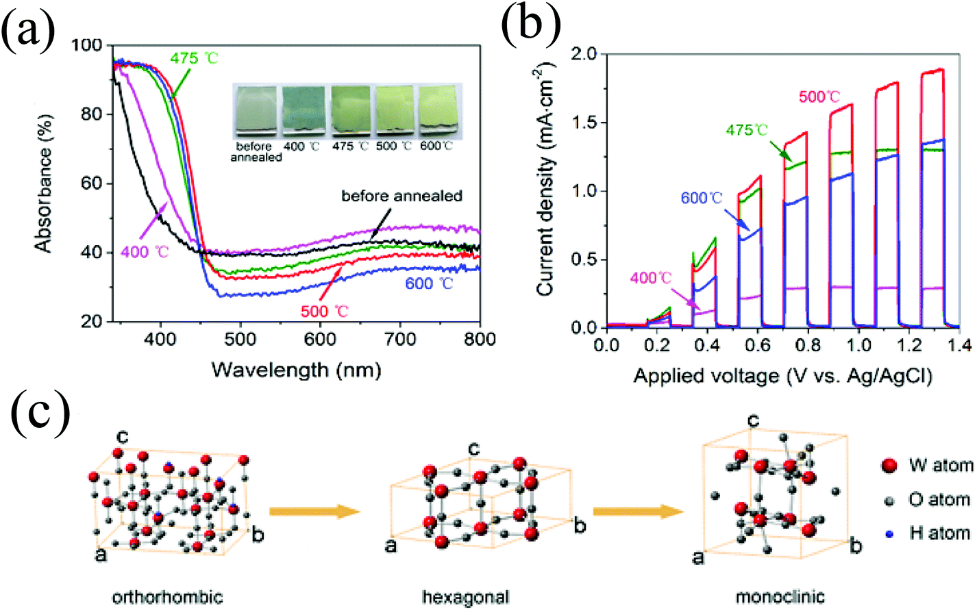 | ||
| Fig. 4 (a) UV–vis absorption spectra of WO3 films before and after annealing at different temperatures. The inset is the corresponding photographs, (b) linear sweep voltammetry of WO3 photoanodes annealed at different temperatures under chopped incident light, (c) schematic illustration of unit cells of orthorhombic WO3·0.33H2O, hexagonal WO3, and monoclinic WO3. Reproduced from ref. 29. Copyright 2016 American Chemical Society. | ||
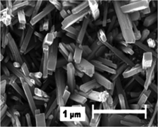
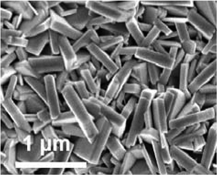
Nayak et al.105 synthesized WO3·H2O nanoplates via a facile precipitation method, which were evolved into WO3 nanowires on subsequent solvothermal treatment (Fig. 5a–d). The WO3·H2O nanoplates had an orthorhombic phase, while WO3 nanowires showed a monoclinic phase (Fig. 5e). The WO3 nanowires exhibited outstanding PEC activity with a photocurrent density ∼21 times higher than the WO3·H2O nanoplates. As discussed above, (section 3.1), the nanoplates (2-D nanostructure) normally have a higher photocurrent value than the nanowire (1-D nanostructure). The significantly enhanced PEC performance of WO3 nanowires was attributed to different phases between WO3·H2O nanoplates and WO3 nanowires. The high crystallinity of WO3 nanowires reduced the interfacial charge transfer resistance, and thereby improved the PEC performance.
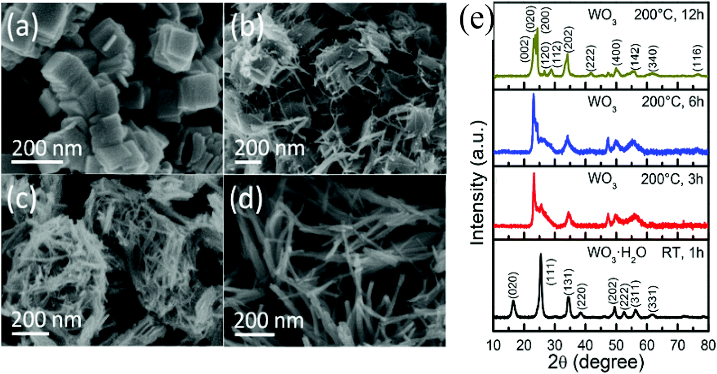 | ||
| Fig. 5 FESEM images of (a) stacked WO3·H2O square nanoplates synthesized at room temperature using 0.025 M of WCl6 solution in ethanol for 1 h. FESEM images of WO3 nanowires evolving from stacked WO3·H2O nanoplates after (b) 3 h, (c) 6 h, and (d) 12 h solvothermal treatment of WO3·H2O nanoplates at 200 °C in ethanol. (e) XRD patterns of these obtained samples. Reproduced from ref. 105. Copyright 2017 American Chemical Society. | ||
Extensive research efforts have been made to explain the effects of crystal phase on the photocatalytic performance. For example, Park et al.82 reported that during the annealing process, with the transformation of the crystal phase, the removal of water induced the surface disorder or oxygen deficiencies of WO3 and thus affected the PEC performance. Zeng's group considered that peroxo species were easily formed on the surface of WO3·H2O due to its inferior crystallinity, while WO3 annealed at 500 °C had the highest current density because of the conversion of exposed (200) facets to highly reactive (002) facets, superior crystallinity and fewer defects to decrease the recombination of electron–hole pairs.41 This suggestion was also confirmed by Su's group.104 Fan's group77 suggested that the monoclinic WO3 obtained at 500 °C (WO3-500) exhibited a red shift of the absorption edge which effectively separated the photoexcited electrons and holes and migrated the carriers to the photoanode surface. The presence of both orthorhombic and monoclinic phases along with defects for the WO3-450 sample and the collapse of nanorods for WO3-550 restricted the efficient separation and migration of charge carriers. Yang et al. attributed the enhanced PEC properties to the higher crystallinity and the reduced PEC properties for WO3 calcined at temperatures higher than 500 °C to the highly damaged surface of the platelets.64 The improved crystallinity via high calcination temperature facilitating a better charge separation was also proved by Nuraje's group in the photocatalysis of SrTiO3.23 Thus, it can be concluded that the as-prepared hydrated tungsten oxide needs to be calcined at 500 °C to obtain monoclinic WO3 for an optimal PEC.
3.3. Engineering of crystalline structures
Recent studies on semiconductor surface engineering have demonstrated that photoexcited electrons and holes can be driven by different crystal planes. Therefore, certain crystal faces of semiconductors will be preferentially reduced, while other crystal faces are preferentially oxidized.106 Controlling and exposing some high energy crystal surfaces can improve the photocatalytic and PEC efficiency of photoelectrodes.107,108 Compared with the (200) facet (1.43 J m−2) and the (020) facet (1.54 J m−2), the (002) facet of WO3 possesses the highest surface energy (1.56 J m−2),109 which is more favorable for adsorbing the reaction species on the (002) facet to decrease the surface energy. It is verified by Wang et al. through density functional theory (DFT) calculations.32 Due to the weakest W–O bond in the monoclinic WO3, the dangling O atoms on the (002) crystal plane could provide more abundant active sites for H2O and organics through the hydrogen bond. Therefore, photo-excited holes are more easily consumed on the (002) crystal plane involving the oxidation of water and the degradation of organics by generating active oxygen species, thereby impeding the recombination of photogenerated electrons and holes. Consequently, the exposure of highly reactive facets could effectively improve the PEC performance in water splitting and the degradation activity of organic pollution.92,110,111Zeng's group41 prepared WO3 nanoplate array film photoanodes with a preferential orientation of highly reactive (002) facets by the reduction of peroxotungstates. The effects of synthesis time, temperature, and the amount of the capping agent on the morphologies and nanostructures of the as-prepared WO3 films were discussed. The TEM images and SAED patterns indicated that the WO3·H2O plates grew along the crystal of (020) face which were converted into WO3 plates with preferentially exposed (002) facets via annealing. The sample annealed at 500 °C exhibited the highest photocurrent density which was ∼1.42 mA cm−2 at 1.23 V vs. RHE. The enhanced performance of PEC water splitting was ascribable to the superior crystallinity which could impede the formation of peroxo species on the surface of WO3. The exposed highly reactive (002) facets of WO3 nanoplates significantly improved the performance of PEC water splitting. WO3 photoanodes decorated with a Co–Pi co-catalyst improved the water oxidation kinetics and reduced the photocorrosion resistance. Zhang et al.92 synthesized monoclinic WO3 nanomultilayers with (002) facets exposed via a solvothermal method. The sandwiched WO3 nanomultilayers exhibited photocurrent densities higher than the WO3 nanorods synthesized as a reference. The specific surface area of WO3 nanorods and nanomultilayers indicated that morphology is not the decisive factor for the enhanced photocurrent of the nanomultilayers. It is the preferentially exposed highly reactive (002) facets of WO3 nanomultilayers that contributed to the improved PEC water splitting performance.
Although WO3 exhibits high stability and resistance against photo-corrosion in acids under solar illumination,52,92 WO3 nanostructures still suffer from photocorrosion and photocatalytic deactivation because of the formation and accumulation of peroxo species on the surface of WO3.33,59,112 In PEC water splitting, photogenerated holes can cause a series of oxidation reactions, including the oxidation of surface hydroxyl groups of WO3 or the oxidation of water/hydroxide. During the water oxidation reaction, oxygen and peroxo species will be formed. Thermodynamically, the photo-oxidation of water to oxygen (E° = 1.23 V) is more feasible than the formation of peroxo species (E° = 1.78 V). However, the peroxo species become kinetically competitive with oxygen evolution because of the slow kinetics of the oxygen evolution reaction. More importantly, the formation of peroxo species at the WO3 surface can cause an obvious alternate photo-oxidation reaction, which may result in the loss of photoactivity or photodissolution of WO3. To address the aforementioned issues, Wang et al.32 synthesized WO3 nanoplates with highly reactive (002) oriented facets via a 2-step hydrothermal method and evaluated the PEC conversion performance (Fig. 6a–f). The 1-step-16 h WO3 nanoplates were prepared via a hydrothermal method for 16 h, while the 2-step-16 h WO3 nanoplates were obtained through the 1-step-8 h WO3 nanoplates after hydrothermal treatment for another 8 h. All of the nanoplates were composed of dense and vertically aligned nanoplate arrays (Fig. 6a–c). The XRD spectra show that the 1-step-16 h WO3 nanoplates were mainly exposed (200) facets (Fig. 6d) and the 2-step-16 h WO3 nanoplates were enriched (002) facets (Fig. 6f). During the 1-step-16 h hydrothermal reaction, the WO3 nanoplates mainly had the exposed (002) facets at the initial 8 h of hydrothermal reaction and were then converted into (200) facets exposed in the subsequent 8 h of hydrothermal reaction. This transformation can be explained by the theory of dissolution and recrystallization. Different from the 1-step-16 h WO3 nanoplates, only a partial recrystallization occurred for the 2-step-16 h WO3 nanoplates, which resulted in a larger (200)/(002) ratio. The prepared 2-step-16 h WO3 nanoplates exhibited a remarkable photocurrent density of 3.7 mA cm−1 (1.23 V vs. RHE) which corresponded to ∼93% of the theoretical photocurrent of WO3 (Fig. 6g). The curves of chopped transient photocurrent density vs. time showed that the WO3 nanoplates prepared by a 2-step hydrothermal method exhibited the highest photocurrent density and the best stability (Fig. 6h). DFT calculations together with experimental studies demonstrated that the exposing highly reactive (002) facet and nanoplate structures facilitated the separation of photoelectron–hole pairs and suppressed the formation of peroxo-species on the surface, and thus enhanced the PEC activity and retained a better photo-stability (Fig. 6i). As a result, the highly oriented (002) crystal plane could significantly improve the PEC water splitting performance and the stability. Accompanied by the 2-D nanostructure and highly active crystal monoclinic phase, more research should be focused on the use of 2-D monoclinic WO3 with a preferentially exposed (002) crystal plane for PEC water splitting in the future.
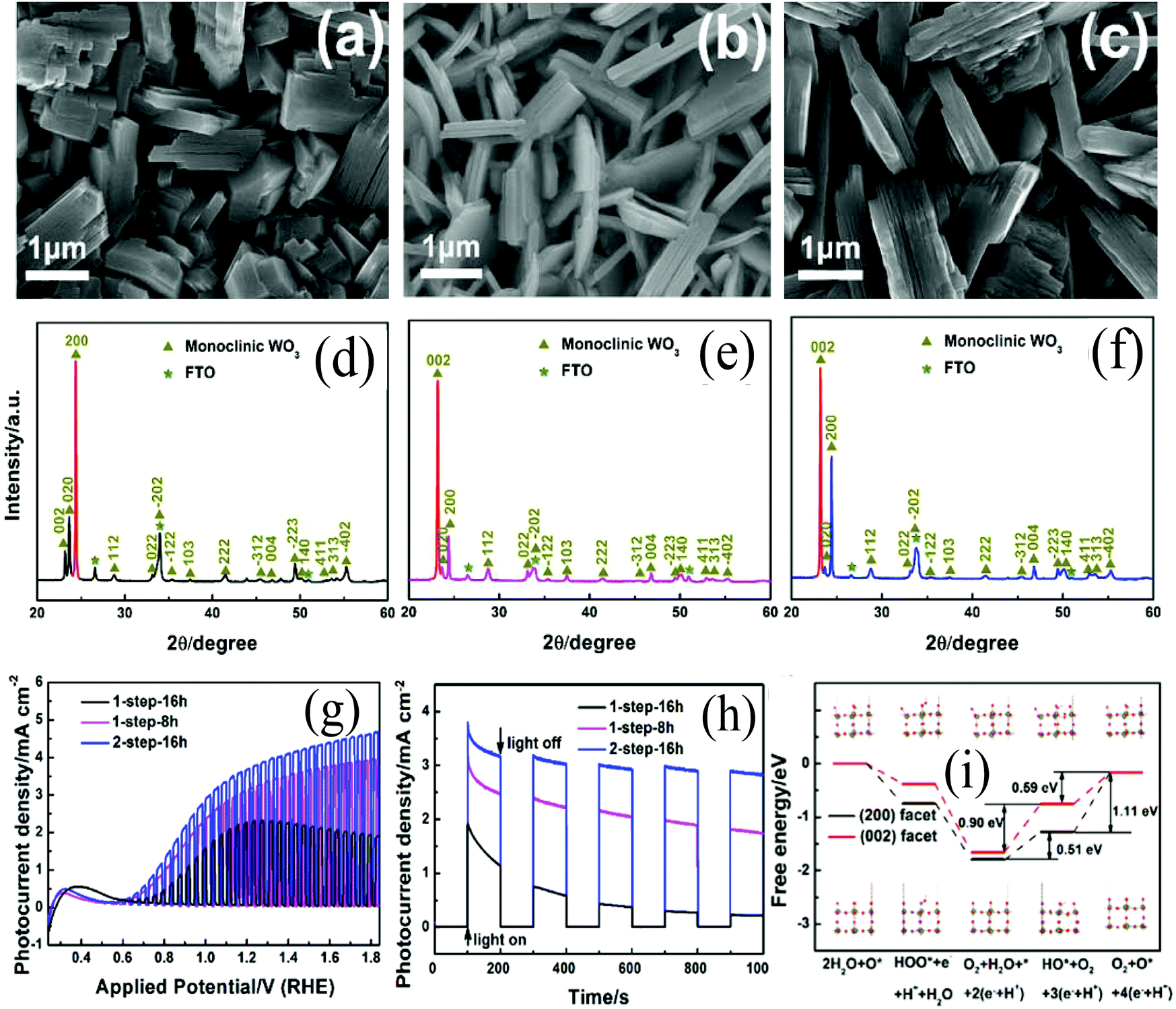 | ||
| Fig. 6 FESEM images and XRD patterns of (a, d) 1-step-16 h, (b, e) 1-step-8 h, (c, f) 2-step-16 h photoanodes prepared by the hydrothermal method, (g) photocurrent density vs. applied potential curves, (h) photocurrent density vs. time measured at 1.23 V vs. RHE, and (i) free energy diagram of the (200) facet and (002) facet at the potential of 1.23 V. Insets: The models that show the surface status of every reaction step: tungsten atoms are represented by gray spheres, oxygen atoms by red spheres, and protons by white spheres, while oxygen gas is not shown in the models. Reproduced from ref. 32. Copyright 2016 Elsevier. | ||
3.4. Forming composites or heterojunctions
Since pristine WO3 nanomaterials suffer from low solar spectrum absorption (about 12%), slow charge transfer at the electrode/electrolyte interface and rapid electron–hole recombination, it is of great interest to address these problems to improve the photoelectrocatalytic properties of WO3 by constructing heterojunctions. By connecting two n-type materials with similar CB and VB energies, one can create a type II heterojunction which can localize electron and hole wave functions in the core or shell material, and thereby improve the charge separation.113,114 Otherwise, coupling an n-type semiconductor together with a p-type semiconductor to create p–n junctions115 or Z-scheme systems can significantly promote efficient charge separation. To date, a variety of semiconductors are coupled with WO3 to construct a heterojunction, such as WO3/Bi2MoO6,116 α-Fe2O3/WO3,117,118 WO3/CuWO4,85,119 NiWO4/WO3,120 Bi2S3/WO3,121 WO3/BiVO4,122–125 WO3/TiO2,113,126 ZnWO4/WO3,127 and NiO/WO3,128 to enhance the photocatalyst or photoelectric conversion performance. Part of the binary heterojunction, fabrication methods and their PEC water splitting performance are summarized in Table 2. Some ternary heterojunction structures, such as WO3/rGO/Sb2S3,129 where rGO serves as the conductive layer, have been reported to enhance the charge transfer. A variety of semiconductors with conduction and valence band energies vs. NHE are shown in Fig. 7a. It is well known that the band gap positions and the Fermi level directly determine the electron transport in the heterostructure systems. In the case of WO3, coupling with a narrow band gap semiconductor to form a type II heterojunction is an effective way to improve the photocatalytic performance. Normally, the photogenerated electrons could be easily transferred from the CB of the secondary material to the CB of WO3 while driving photogenerated holes from the VB of WO3 to the VB of a coupled semiconductor which possesses a narrower band gap energy (Fig. 7b). Different from the n-type semiconductors where electrons are employed as the photogenerated carriers, the number of holes is much larger than that of electrons for p-type semiconductors. Therefore, in p–n type heterojunctions or Z-scheme systems, the photo-excited electrons from the CB of WO3 can readily recombine with the photogenerated holes from the VB of the p-type semiconductor. It is significant to optimize the reduction and oxidation ability for the PEC water splitting (Fig. 7c).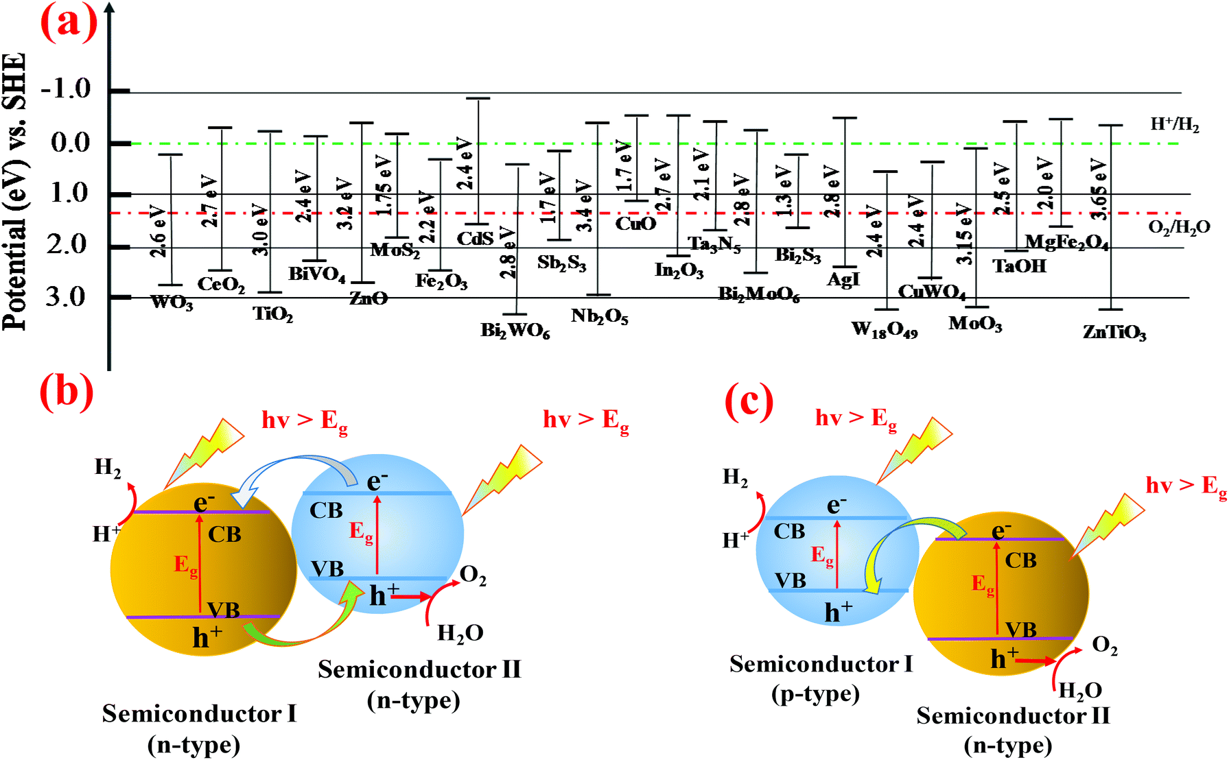 | ||
| Fig. 7 (a) Bandgap energy, VB and CB positions of several semiconductors on a potential scale (V) vs. NHE/vacuum. (b) Schematic illustration of type II heterojunction and (c) p–n junction band alignments, and the correspondingly possible photoexcited electron–hole pair separation and transfer between the contacted semiconductors. | ||
| Heterostructure | Fabrication method | SEM/TEM image | Photoelectrochemistry | Ref. |
|---|---|---|---|---|
| CuWO4/WO3 | Hydrothermal and then dipping-annealing process |
|
Photocurrent: 1.21 mA cm−2 (WO3: 0.64 mA cm−2) at 1.5 V vs. Ag/AgCl; IPCE: 55.3% at ∼350 nm at 1.2 V vs. Ag/AgCl; electrolyte: 0.2 M Na2SO4 | 85 |
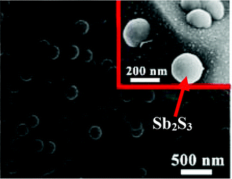
| WO3/Sb2S3 | Hydrothermal |
|
Photocurrent: 1.79 mA cm−2 at 0.8 V vs. RHE; IPCE: ∼12.5% at 300 nm at 0.8 V vs. RHE; electrolyte: 1 M H2SO4 | 39 |
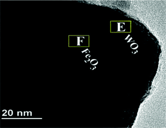
| α-Fe2O3/WO3 | Hydrothermal and then followed by deposition-annealing |
|
Photocurrent: 1 mA cm−2 (WO3: 0.36 mA cm−2) at 1.23 V vs. RHE; IPCE: 30.4% at ∼330 nm at 1.23 V vs. RHE; electrolyte: 0.1 M Na2SO4 | 117 |
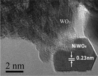
| NiWO4/WO3 | Hydrothermal and followed by deposition-annealing |
|
Photocurrent: 0.44 mA cm−2 (WO3: ∼0.25 mA cm−2) at 1.4 V vs. Ag/AgCl; IPCE: 40.7% at 340 nm at 1.2 V vs. Ag/AgCl; electrolyte: 0.2 M Na2SO4 | 120 |
| WO3/Cu2O | Hydrothermal and then followed by electrodeposition |
|
Photocurrent: 1.37 mA cm−2 (WO3: 0.39 mA cm−2) at 0.8 V vs. RHE; IPCE: 10.7% at ∼300 nm at 0.8 V vs. RHE; electrolyte: 1 M H2SO4 | 130 |
| WO3/Bi2S3 | Hydrothermal and followed by chemical bath deposition |
|
Photocurrent: 5.95 mA cm−2 (WO3: 0.17 mA cm−2) at 0.9 V vs. RHE; IPCE: 68.8% at ∼435 nm at 0.9 V vs. RHE; electrolyte: 0.1 M Na2S + 0.1 M Na2SO3 | 131 |
| WO3/BiVO4 | Soaking hydrothermal-calcining |
|
Photocurrent: 2.92 mA cm−2 at 1.81 V vs. RHE; electrolyte: 0.5 M KH2PO4 | 132 |
| WO3/FeOOH | Spray pyrolysis deposition and followed by electrodeposition |
|
Photocurrent: 1.4 mA cm−2 (WO3: 0.8 mA cm−2) at 1.23 V vs. RHE; electrolyte: 0.5 M K2SO4 | 133 |
| WO3/BiVO4 | Hydrothermal and followed by spin coating |
|
Photocurrent: 3.17 mA cm−2 (WO3: 1.41 mA cm−2) at 1.23 V vs. RHE; electrolyte: 0.1 M Na2SO4 | 134 |
| WO3/BiVO4 | Solvothermal followed by spin-coating |
|
Photocurrent: 1.6 mA cm−2 (WO3: 0.4 mA cm−2) at 1 V vs. RHE; IPCE: 31% at ∼420 nm at 0.5 V vs. RHE; electrolyte: 0.5 M Na2SO4 | 135 |
| WO3/FeOOH | Hydrothermal and followed by electrodeposition |
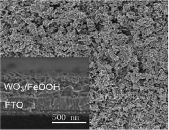
|
Photocurrent: 1.3 mA cm−2 (WO3: 0.6 mA cm−2) at 1.23 V vs. RHE; electrolyte: 0.1 M KPi buffer | 136 |
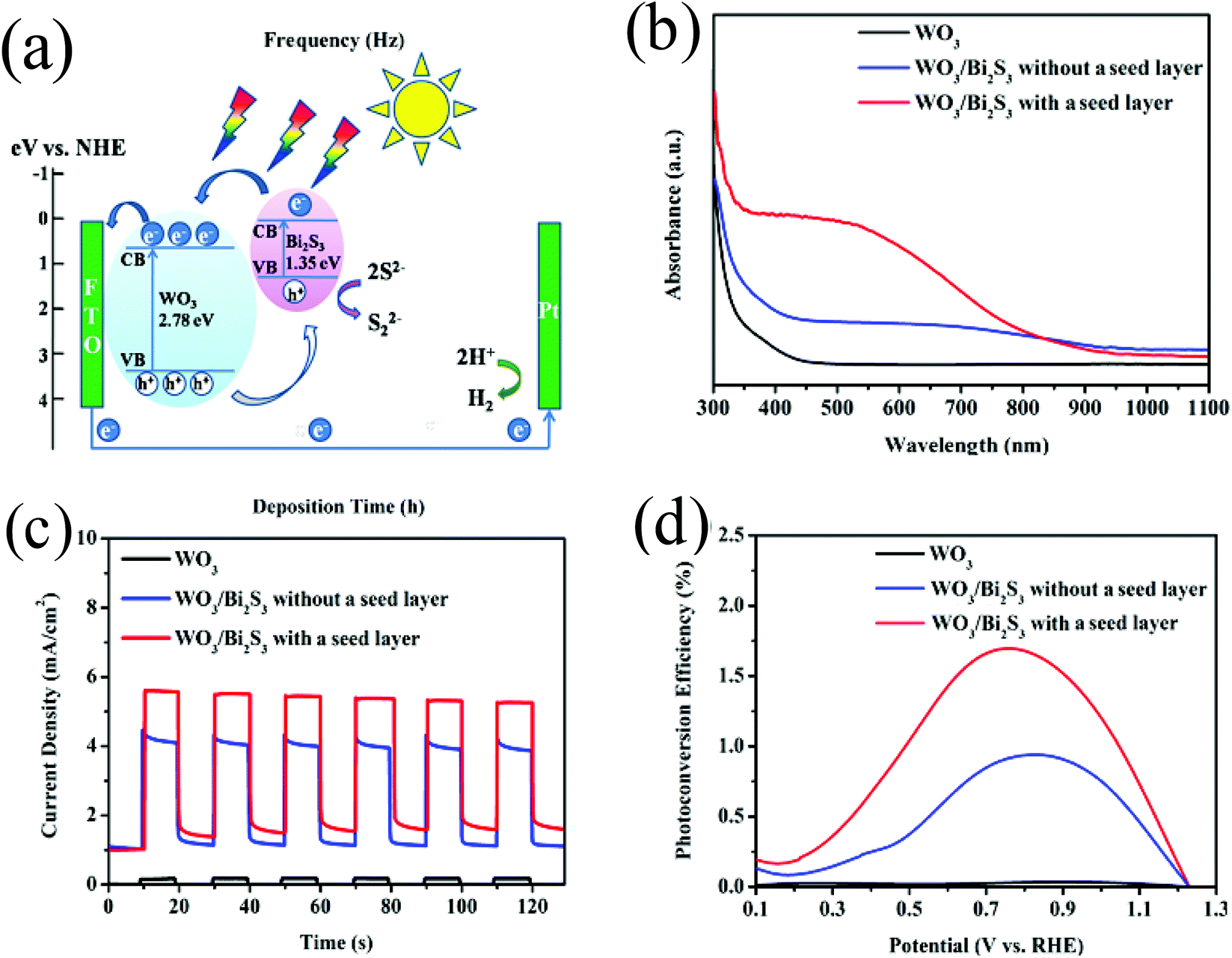 | ||
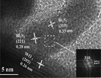
| Fig. 8 (a) Schematic of the WO3/Bi2S3 heterojunction and the reaction process in the PEC cell, (b) UV-vis absorption spectra of bare WO3 (black), WO3/Bi2S3 without a seed layer (blue) and WO3/Bi2S3 with a seed layer (red), (c) I–t curves of bare WO3 (black), WO3/Bi2S3 without a seed layer (blue), and WO3/Bi2S3 with a seed layer (red) at 0.9 V vs. RHE, (d) photoconversion efficiency of pristine WO3 (black), WO3/Bi2S3 without a seed layer (blue), and WO3/Bi2S3 with a seed layer (red) Reproduced from ref. 131. Copyright 2017 American Chemical Society. | ||
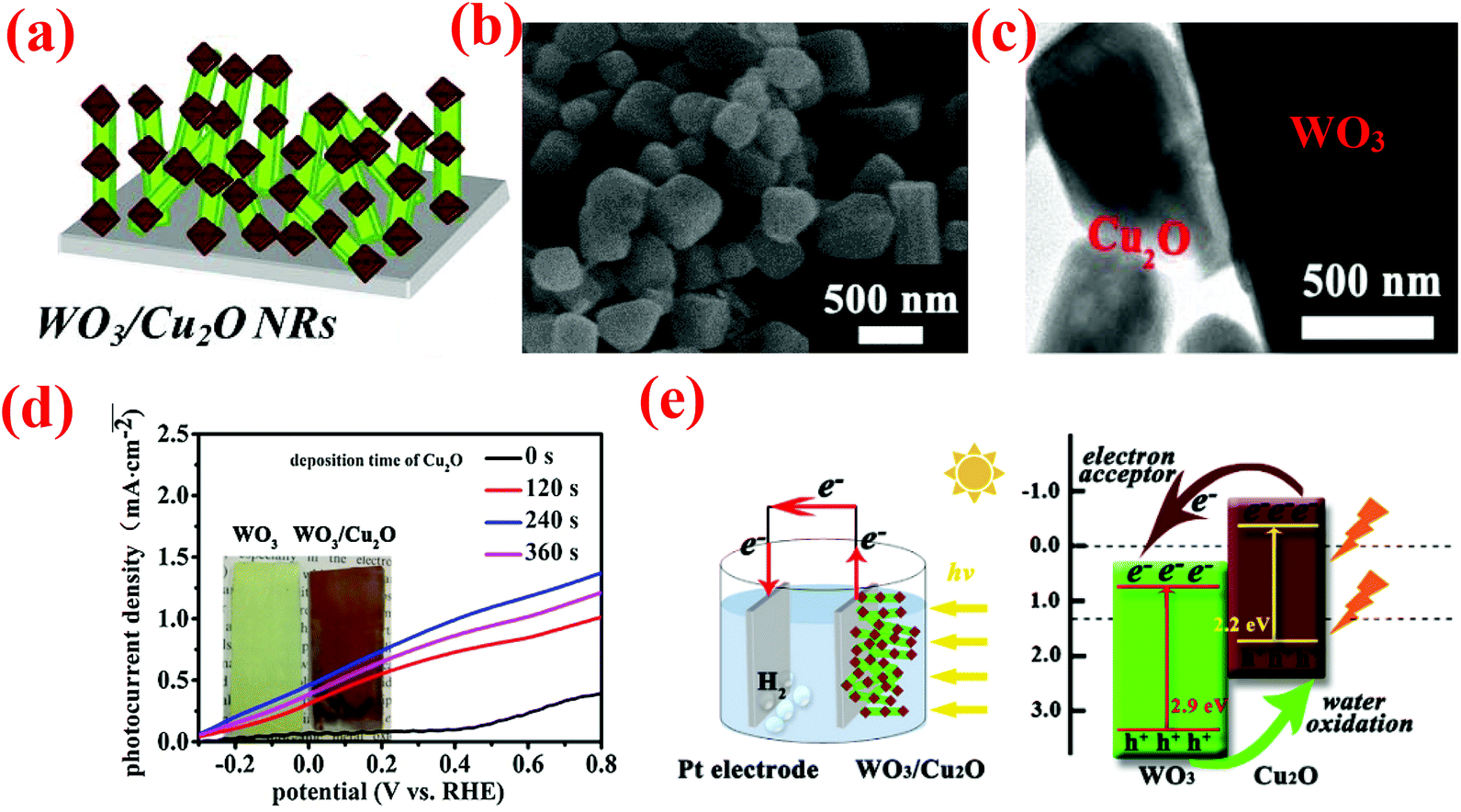 | ||
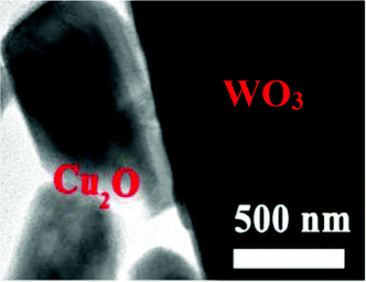
| Fig. 9 (a) Schematic of WO3NRs/Cu2O array electrodes, (b) typical top view SEM images of WO3NRs/Cu2O, (c) TEM images of WO3NR/Cu2O arrays, (d) the photocurrent density–voltage curves of the samples, (e) schematic of the WO3NR/Cu2O array heterojunction photoanode applied in overall water splitting and simplified schematic illustration of the band-gap energy diagram, showing the enhanced light-harvesting and charge-transfer processes. Reproduced from ref. 130. Copyright 2017 Elsevier. | ||
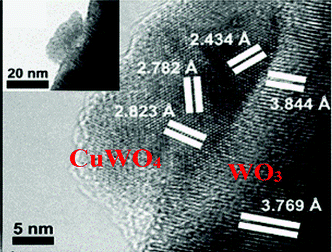
Zhan et al.85 fabricated CuWO4/WO3 heterojunction photoanodes and demonstrated that coupling with CuWO4 enhanced the photocurrent density of WO3 due to the extension of visible light response, efficient separation of photo-excited carriers at the WO3/CuWO4 interface and better electron transport properties. The WO3 decorated with the exfoliated Bi2MoO6 nanosheets showed a satisfactory photocurrent density of 2.2 mA cm−2 at 0.8 V vs. SCE compared to WO3 (1.1 mA cm−2). The improved PEC performance of the WO3/Bi2MoO6 heterojunction could be attributed to the suitable band position between WO3 and Bi2MoO6 that facilitated the electron–hole separation and charge transfer. The uniformly exfoliated nanosheets coated on the WO3 surface could also provide a high electric mobility.116
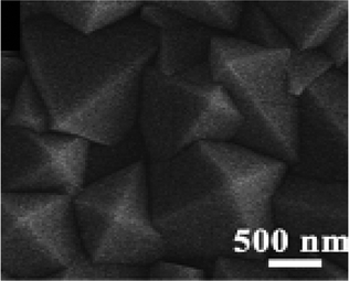
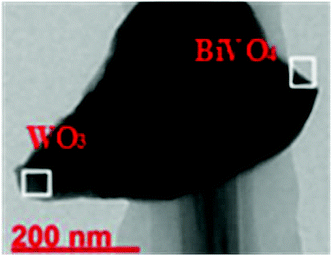
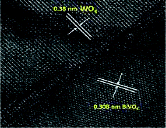
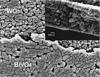
It is an appealing way to enhance the performance of PEC water splitting by designing special nanostructure semiconductor composites. The core–shell structure is reported to be an efficient system to maximize each separate process optimally which is beneficial for water splitting performance.84,104,113,124,135 By increasing the surface and interface area of the WO3/BiVO4 heterojunction, the core–shell heterojunction of WO3/BiVO4 promoted the generation and separation of photoexcited electrons and holes. The framework of the core–shell nanostructure can capture multiple reflections of sunlight owing to its cavity which is beneficial for an efficient utilization of solar photons to improve the photocatalytic activity.142 Therefore, it is critical to develop an optimized WO3/BiVO4 core–shell heterojunction to enhance the PEC water splitting properties. Rao et al.124 synthesized a core–shell structure photoanode incorporated with W-doped BiVO4 and WO3. The as-prepared sample exhibited excellent PEC water splitting properties with a high charge separation and surface transfer efficiency. Due to the short hole diffusion length attributed from the core–shell structure, the holes generated in the BiVO4 shell can readily reach the semiconductor/electrolyte interface and thereby improve the photoelectric conversion efficiency. Jin's group142 prepared yolk–shell structured WO3/BiVO4 heterojunctions with BiVO4 coating onto the surface and inside of WO3 shells. As shown in Fig. 10a–f, the hollow WO3 structure, yolk–shell WO3 spheres and yolk–shell WO3/BiVO4 heterojunctions were clearly observed. The HR-TEM image (Fig. 10f) and the corresponding energy-dispersive X-ray (EDX) elemental mapping (Fig. 10g–j) indicated the intimate contact in the WO3/BiVO4 heterojunction structure. Compared with hollow WO3, the enhanced photoelectrocatalytic properties of the yolk–shell WO3 were attributed to the particular yolk–shell structure with a beneficial higher charge-carrier separation and a restricted recombination of the photogenerated electrons and holes. After introducing the FeOOH/NiOOH layer as an oxygen evolution reaction (OER) co-catalyst on the surface of the yolk–shell WO3/BiVO4 heterojunction, the composites showed a strong negative shift in the photocurrent onset potential and exhibited the highest photocurrent density (Fig. 10k). In this yolk–shell WO3/BiVO4/OER heterojunction, the yolk–shell WO3 served as an electron conductor while BiVO4 functioned as the main light absorber to form a type-II heterojunction structure. The photogenerated electrons migrated from the CB of BiVO4 to the CB of WO3. On the other hand, the photogenerated holes left in the VB of WO3 were injected into the VB of BiVO4. This process greatly improved the charge transfer and reduced the recombination of photoexcited electrons and holes. The OER co-catalyst layer reduced the overpotential of water oxidation and subsequently improved the PEC water splitting performance.
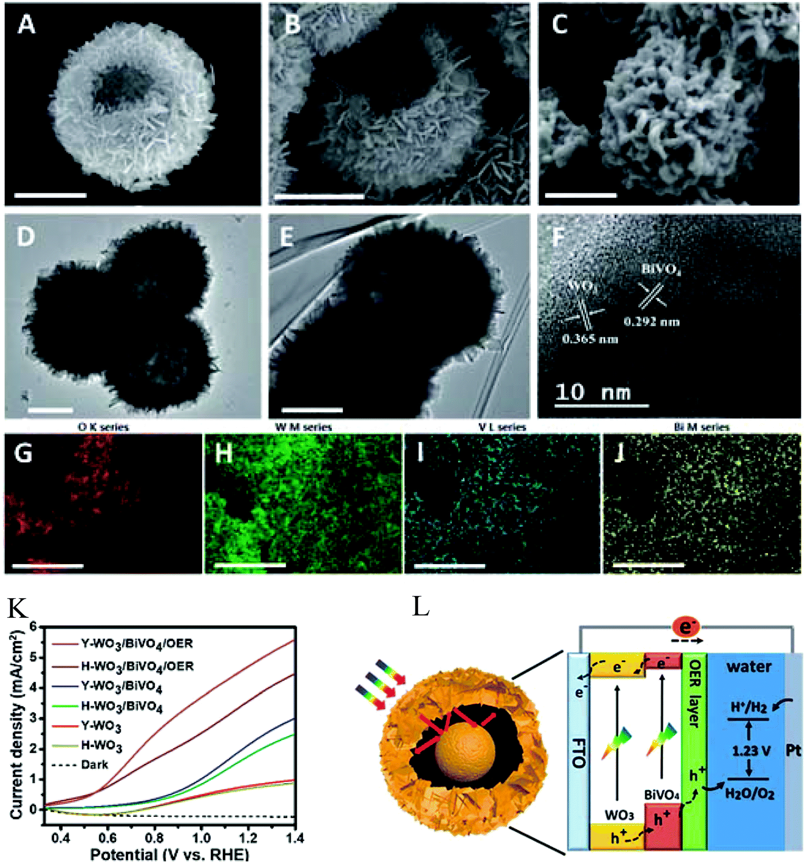 | ||
| Fig. 10 SEM and TEM images of the hollow WO3 (A and D) and yolk–shell WO3 (B and E), (C and F) SEM and HR-TEM images of the yolk–shell WO3/BiVO4 heterojunction, (G–J) the corresponding EDX elemental mapping of the yolk–shell WO3/BiVO4 (scale bars are 1 mm), (K) linear sweep voltammetry (LSV) curves of the samples in 0.5 M Na2SO4 solution under AM 1.5G light illumination, (L) schematic diagram for the construction of the yolk–shell WO3/BiVO4/OER photoanode and the energy diagram for PEC water splitting. Reproduced from ref. 142. Copyright 2018 Royal Society of Chemistry. | ||
3.5. Construction of cocatalysts
170 have served as OEC for the photocatalytic O2 production. Amongst them, Co–Pi has received much attention due to its outstanding OER performance.171,172 Seabold and co-workers40 coupled WO3 with a layer of Co–Pi to improve the photostability of WO3 photoanodes and enhanced the photo-oxidation reaction. After photocurrent measurement for 2 h, the appearance of pores and the decrease of crystal grains of the WO3 electrode indicate that the OER is not the sole photo-oxidation reaction occurring at the bare WO3 electrode. Peroxo species at the WO3 surface were formed resulting in a loss of PEC activity of the bare WO3 electrode. After the deposition of the Co–Pi OEC layer on the WO3 electrodes, the photocurrent remained stable over long time since Co–Pi OEC effectively inhibited the formation of peroxo species at the surface and prevented the photochemical deactivation of WO3. Fan et al.77 proposed a rational design via combining WO3 and NiFe-layered double hydroxide (LDH) nanoarrays. The WO3 nanorod arrays were prepared via a hydrothermal process and decorated with a NiFe-LDH by electrochemical deposition (Fig. 11a–c). They found that the deposition time of the NiFe-LDH significantly affected the PEC performances and obtained the best performance measured for the WO3@NiFe-LDH-200s sample. The as-prepared sample exhibited excellent photocurrent density and higher stability compared with bare WO3 nanorods (Fig. 11d). As an efficient OER catalyst, the NiFe-LDH could effectively facilitate the separation of photogenerated electron–hole pairs and enhanced water splitting kinetics. After coupling with the NiFe-LDH, the photoexcited holes in WO3 preferentially oxidized the low valence NiII in the redox couples of LDH to the high valence NiIII,IV, and then the high valence NiIII,IV further oxidized water to release oxygen. This oxidation process has been demonstrated to be kinetically faster than water oxidation directly via photogenerated holes (Fig. 11e). Due to the promotion of water splitting kinetics and hindering of the charge recombination, the WO3@NiFe-LDH-200s sample exhibited a superior PEC water oxidation performance. However, a thick OEC layer inevitably blocked the incident light and reduced the PEC activity of WO3.32,40 It is highly desirable to improve the stability of the WO3 photoanode without sacrificing the photocatalytic activity.
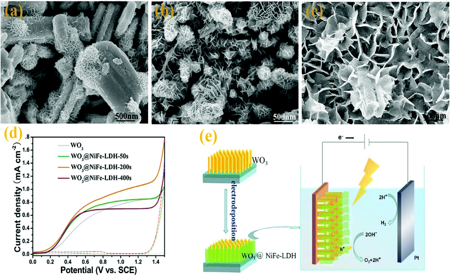 | ||
| Fig. 11 SEM images of WO3@NiFe-LDH NR arrays obtained with various electrodeposition durations: (a) 50 s, (b) 200 s, (c) 400 s, (d) linear sweep voltammograms at a scan rate of 10 mV s−1 (solid line: under visible light, dashed line: in dark) and (e) PEC water oxidation mechanism on the WO3@NiFe-LDH NR arrays under visible light. Reproduced from ref. 77. Copyright 2016 Elsevier. | ||
3.6. Doping or oxygen deficiency
There exist two main kinds of defects in WO3. One is oxygen deficiency, which accelerates the charge carrier transfer at an optimized amount.173,174 The other is the trap states that promote the recombination of electrons and holes. Serving as shallow donors, the bulk oxygen vacancies can improve electrical conductivity and facilitate charge transfer, while surface oxygen vacancies introduce a large number of defects which can be the center of recombination of photogenerated electron–hole pairs and thereby reduce the PEC performance.38 Therefore, it is one of the key objectives to reduce the surface oxygen vacancies without affecting the bulk oxygen vacancies. Li et al. synthesized a series of substoichiometric WO3−x nanoflakes and demonstrated that the enhanced photocurrent density was related to the increased donor density after introducing oxygen vacancies. The observed anodic shift of the hydrogen-treated samples was due to excess surface oxygen vacancies which aggravated the charge carrier recombination.33 Li et al. introduced oxygen vacancies by adding TiCl3. They demonstrated that the oxygen vacancies were introduced in proportion to the concentration of TiCl3. Treatment by TiCl3 at high concentration led to excess surface oxygen vacancies that resulted in a thicker disorder layer with more recombination centers.175 Similar results were obtained by the treatment of WO3via H2O2 to introduce surface oxygen vacancies.176 Gong et al.67 synthesized WO3 nanoflake photoanodes with decreased surface oxygen vacancies but suitable bulk oxygen vacancies by a facile hydrogen annealing followed by an ozone treatment (named HO-WO3). The remarkable enhancement in the photocurrent values from 1.09 mA cm−2 for pristine WO3 to 2.25 mA cm−2 for the HO-WO3 sample at 1.23 V vs. RHE was achieved. The improved performance of the HO-WO3 sample was due to the increased bulk oxygen vacancies that served as shallow electron donors to enhance the conductivity of WO3 and the decreased surface oxygen vacancies that reduced the recombination of photogenerated electrons and holes. However, the introduction of oxygen vacancies using hydrogen treatment resulted in high consumption of hydrogen gas, which hindered their applications in practical fields.Concerning the traps, modifying the passivation layer on the surface of semiconductor particles can inhibit the recombination of photogenerated electrons and holes. Doping with a hetero-element can extend the photoresponse range and increase the carrier concentration. However, due to different radii between the donor atom and the host atom, the introduction of a dopant will cause a significant increase of lattice distortion and thus results in the increase of carrier recombination centers.177–179 Doping with a hetero-element will decrease the solubility of dopant species and reduce the structural stabilities.179,180 Therefore, it is the most critical issue to select the optimized doping element leading to an inconspicuous structural disturbance and sparse defect sites. Transition metals and lanthanides are able to intercept the electronic structure of WO3 to extract more visible solar spectra.181 Doping Ti4+ into the WO3 semiconductor is a feasible way to improve the PEC performance because impurity states between the CB and VB of WO3 change the band structure of WO3. Meanwhile, similar radii of the guest and the host result in less lattice distortion.182 Yb, as one of the lanthanides, is an electron-rich f-orbital element which increases the charge carrier generation for the enhanced photocurrent densities in WO3. Liew et al.181 synthesized Yb-doped WO3 photocatalysts by the method of co-sputtering of WO3 and Yb. They demonstrated that the samples prepared under W and Yb sputtering powers of 100 W and 5 W, respectively, exhibited the highest photocurrent density. As the ionic radius of Yb3+ is 28% larger than that of W6+, it is easier for Yb3+ to contribute electrons from its outer shell 4f13 to the conductive carrier path in WO3 which is beneficial for reducing the charge transfer resistances and enhancing the efficiency of charge transfer at the photocatalyst/electrolyte interface. Nevertheless, excess Yb3+ caused higher densities of grain boundary which acted as carrier recombination centers to reduce the hole–electron separation efficiency. Other metals, such as Bi,183 Al,184 Ni,185 Co,186 and Mo,187 were employed as dopants for WO3 to enhance the PEC water splitting performance. Since the introduction of metal elements into semiconducting oxides reduced the thermal stability, doping of nonmetal elements has attracted considerable attention.188 Doping N into WO3 significantly narrowed the band gap of WO3 to a value lower than 2.0 eV and thereby greatly enhanced the photo-absorption performance.189 In S-doped WO3, some S atoms replaced O atoms on the surface of WO3 and some S6+ more favorably substituted W6+ to form W–O–S bonds.190 Oxygen vacancies increased to reduce the resistivity and increased the extrinsic absorption. Thus, it significantly increased the absorption of visible light and enhanced the PEC water splitting performance. Despite the fact that doping is an effective strategy to introduce oxygen vacancies and enhance visible light absorption, doping with hetero-elements resulted in a highly defective lattice and seriously limited their practical applications.
4. Z-Scheme water splitting
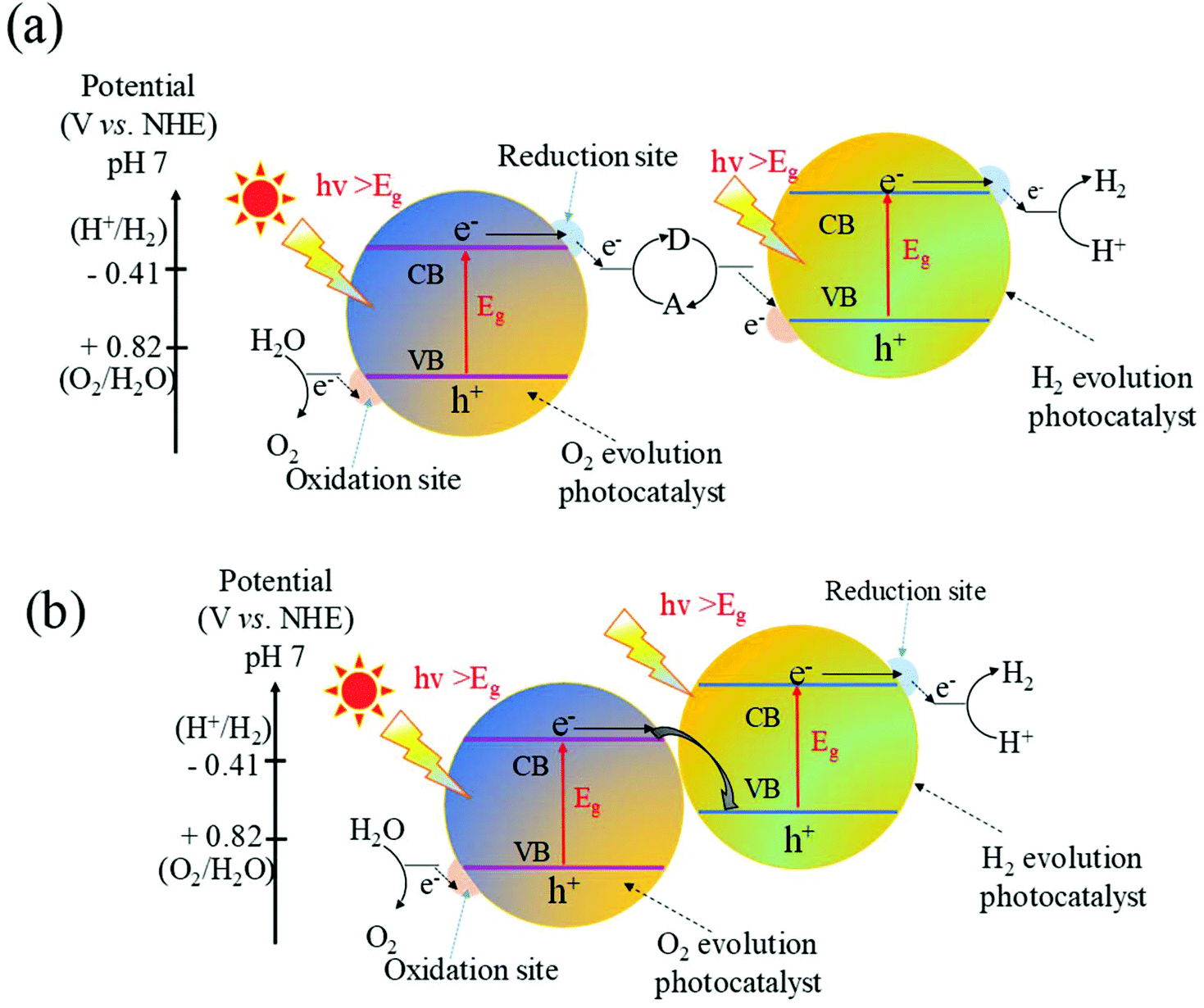
Although coupling with other n-type semiconductors to form type II heterojunctions can significantly improve the photocatalytic performance of WO3, to achieve overall water splitting is limited without changing the original oxidation and reduction potential. Recently, inspired by natural photosynthesis in green plants, great attention has been paid to construct Z-scheme heterojunctions for the overall water splitting under visible light irradiation due to their efficient photogenerated electron–hole separation and optimized redox ability of the photocatalytic system.191–194 Yousaf et al.195 constructed efficient Z-scheme junctions consisting of oxygen-deficient WO3−x nanorods and Zn0.3Cd0.7S nanoparticles and found that H2 was produced in a repeatable manner from aqueous solutions containing Na2SO3 and Na2S as sacrificial reagents without electric energy. Zhu et al.196 prepared carbon nanodots (CNDs) from glucose via a simple hydrothermal process and found that the CNDs without any modification and doping could produce relatively low hydrogen under xenon lamp irradiation. More importantly, after combining with WO3 to form a Z-scheme through an IO3−/I− shuttle redox mediator, the H2 evolution rates of the as-prepared CND/WO3 Z-scheme reached up to 1330 μmol g−1 h−1, which was about 286 times higher than that of pure CNDs.Although the more positive VB than the oxygen generation potential makes WO3 suitable for oxidizing water to generate oxygen, the positive position of the CB limits the reduction of H+ to H2. Thus, WO3 cannot be used for overall water splitting. A strategy to overcome the inherent limits is to introduce Z-scheme junctions to produce hydrogen from water splitting. The fundamental principle of the Z-scheme water splitting is shown in Fig. 12a. In this system, semiconductor I with the CB more negative than the hydrogen generation potential is combined with semiconductor II with the VB more positive than the oxygen generation potential through an appropriate shuttle redox mediator. Compared with one-step water splitting systems, Z-scheme junctions utilize visible light more efficiently due to the reduced energy required to drive each photocatalyst. It is thus possible to apply a photocatalyst that has either a water reduction or oxidation potential to one side of the system. A reversible redox mediator, noble metal particle or graphene has been used as the shuttle electron mediator. To date, there have been many reports on the Z-scheme junctions with appropriate shuttle redox mediators for overall water splitting.197–199 However, many problems exist for the Z-scheme photocatalysts with shuttle electron mediators in water splitting, such as the complicated synthesis process, strong photocatalytic backward reaction and the spectral shielding effect by the shuttle redox mediators.200–202
 | ||
| Fig. 12 Schematic illustration of (a) Z-scheme junction band alignments with an appropriate shuttle redox, (b) direct Z-scheme without an electron mediator for overall water splitting. CB, conduction band; VB, valence band; Eg, band gap. | ||
Over the past few decades, the direct Z-scheme has attracted great attention due to its simple synthesis and wide range of light absorption. A schematic illustration of WO3 based direct Z-scheme junctions is shown in Fig. 12b. Both the CB and the VB of the coupled semiconductors are higher than those of WO3. The CB position of the coupled semiconductor is higher than the position of 2H+/H2. Meanwhile, a large quantity of defects could be readily accumulated at the solid–solid heterointerface, which possesses some similar properties to those of a conductor such as analogous energy levels and low electric resistance. These features prompt the interface to be apt to serve as a recombination center of e−–h+ pairs.203 Therefore, the photoexcited electrons with a lower reduction ability migrated from the CB of WO3 to recombine with the photogenerated holes with a lower oxidation ability in the VB of the coupled semiconductor. The left photogenerated electrons and holes are able to keep strong redox states, which are promising for the overall water splitting. It is worth noting that compared to the type II heterojunction, the charge carrier migration is more feasible for the direct Z-scheme photocatalyst that is attributed to the electrostatic attraction between the electrons and holes. Therefore, photogenerated electron–hole pairs are more readily separated in the Z-scheme heterojunctions, and hence the recombination will be significantly suppressed.
The electron spin resonance (ESR) spin-trapping technique with DMPO under visible light illumination is an effective method to confirm the reaction mechanism of the electron–hole separation in the Z-scheme system. Generally, the CB potential of WO3 located at ∼0.71 eV vs. NHE is more positive compared with the reduction potential of active superoxide (˙O2−) (O2/˙O2− = −0.284 eVNHE). Thus, the photo-generated electrons on the surface of WO3 are thermodynamically unable to react with O2 to produce ˙O2−. In other words, negligible signals of DMPO–˙O2− can be found for pure WO3, whereas WO3 can exhibit a clear DMPO–˙OH signal which is ascribed to the more positive VB potential compared with the oxidation of H2O/or OH− to the ˙OH radicals (OH−/˙OH = +2.4 eV). Xiao et al.194 introduced g-C3N4 to combine with WO3 to form a Z-scheme nanojunction. They found that the DMPO–˙O2− signal was only observed over WO3/g-C3N4 and g-C3N4 and the DMPO–˙OH signal was only observed over WO3/g-C3N4 and WO3. This result implies that both ˙O2− radicals and ˙OH radicals can generate over g-C3N4/WO3 heterostructures, whereas WO3 can only produce the ˙O2− radicals and g-C3N4 can only generate the ˙OH radicals. Therefore, in the g-C3N4/WO3 Z-scheme system, electrons on the CB of g-C3N4 retain a high reduction capability to reduce O2 to the ˙O2− radicals as well as the holes on the VB of WO3 still retain sufficient high oxidation capability to oxidize H2O/or OH− to the ˙OH radicals.
Xie et al.204 constructed a CdS/WO3 Z-scheme nanojunction with lactate as the electron donor. The optimized CdS/WO3 Z-scheme nanojunction showed a high rate of H2 evolution without electric energy, which was four times higher than CdS. WO3 exhibited no H2 production performance. The amount of CdS on the surface of WO3 had a significant effect on the properties of the Z-scheme nanojunction, that is, a high amount of CdS hindered the WO3 from absorbing light and generated the recombination center of photogenerated charges, which reduced the photocatalytic activity. After introducing Pt as the cocatalyst to improve the charge transport between CdS and WO3, H2 evolution rates increased up to 2900 μmol g−1 h−1 under visible irradiation, which was about 7.9 times higher than that of the as-prepared CdS/WO3 Z-scheme nanojunction under visible light irradiation. Dai et al.205 introduced diethylenetriamine (EDTA) as the structure-directing agent and designed a direct Z-scheme system of WO3/CdS-EDTA composites to achieve an overall water splitting without using electrical energy. A distinct separation of electrons and holes was observed in the Z-scheme structure, in which the photo-excited electrons in the CB of WO3 recombined with the photo-excited holes in the VB of CdS. This in turn avoided the enriching of holes on the VB of CdS which effectively reduced the photocorrosion of CdS as well as improved the PEC performance.
Graphitic carbon nitride (g-C3N4) is an organic semiconductor, and it has been intensively studied as a novel metal-free photocatalyst owing to its visible-light absorption, narrow band gap, high reduction ability and high chemical stability.206–208 The CB edge potential of g-C3N4 (−1.13 eV)209 is more negative than the potential of 2H+/H2 (−0.41 V vs. NHE at pH 7),210 indicating that H2 can be produced on the surface of g-C3N4. In contrast to WO3, O2 could not be generated on the surface of g-C3N4 because of the more negative VB edge potential (∼1.57 eV)209 than the potential of H2O/O2 (0.82 V vs. NHE).210 The suitable band gap of the CB and VB between WO3 and g-C3N4 offers appropriate driving forces to separate and transfer photogenerated electron–hole pairs and makes it possible to structure Z-scheme semiconductor nanocomposites. Therefore a composite structure is expected to improve the photocatalytic activity of WO3 by increasing the number of photogenerated charge carriers. In recent years, constructing the Z-scheme WO3/g-C3N4 composites has been reported for the complete oxidation of organic compounds or overall water splitting.211–214 In Xiao's work,215 Z-scheme WO3/g-C3N4 composites with hollow microspheres were fabricated by in situ hydrolysis and a polymerization process consecutively. The prepared heterojunction contains numerous interfaces and highly exposed oxidation–reduction active sites. Due to the unique Z-scheme architecture, more incident photons are expected to be trapped in the hollow cavities, and thus contribute to more electrons and holes available for photocatalytic reactions. The photoluminescence (PL) decay profiles show that a prolonged lifetime of ∼2.23 ns for WO3/g-C3N4 compared to ∼1.62 ns for bare WO3 improved the reaction abilities and significantly enhanced the photocatalytic efficiency of WO3/g-C3N4. Cui et al.216 prepared direct Z-scheme WO3/g-C3N4 composites via a facile one-step heating procedure, which exhibited an improved photocatalytic activity. Complexing WO3 with g-C3N4 caused the red shift which promoted the separation of photogenerated electron–hole pairs. Lu and co-workers217 established a system by combining WO3 and g-C3N4. This system showed an enhanced photocurrent compared to pure WO3, which was ascribed to the accelerated charge separation in the heterointerface because of the optimal structure of the direct Z-scheme. Zhao and coworkers209 combined C3N4 and WO3 to form a direct Z-scheme system via a facile hydrothermal method. In this Z-scheme system, accompanied by 1 wt% Pt, as much as 30.3 and 14.8 mmol of H2 and O2 were generated after 20 h of visible light irradiation (λ > 420 nm), while trace amounts of H2 and O2 were detected over pure g-C3N4. After introducing rGO as the electron mediator to generate ternary composites, the as-prepared samples were able to release hydrogen and oxygen under visible light irradiation with a relatively high performance. The apparent quantum yield efficiency of the well-prepared ternary composites was ca. 0.9% while the homologous sample without rGO showed a smaller value (i.e., 0.7%) under monochromatic light at 420 nm. Due to its excellent conductivity, rGO promoted the photoexcited electron transfer from WO3 to the photo-generated holes in C3N4, acting as a promising electron mediator. Peng et al.218 designed a direct Z-scheme g-C3N4/WO3 photocatalyst via partial intercalation of WO3 within g-C3N4 to enhance the activities of photocatalytic H2 production. Scanning transmission electron microscopy (STEM) clearly resolved the well-defined interfaces between g-C3N4 and WO3, which prompted the charge transportation and benefited the recombination of electrons in the CB of WO3 and holes in the VB of g-C3N4. The internal electric field was suggested to provide the force to drive the Z-scheme electron transportation at the interfacial junction. This increased the lifetime of excited electrons in g-C3N4 and excited holes in WO3, therefore, enhancing the photocatalytic efficiency for the overall water splitting.
5. Summary and outlook
Photoelectrochemical water splitting to generate H2 is a promising approach for our future energy sustainability and has attracted remarkable attention in the past decade. Challenges facing today are to develop photoanodes with high efficiency, stability, and low cost in practical applications. WO3 is one of the promising materials for its visible light response, durable and efficient operation in aqueous solution. Boosting the PEC water splitting performance of WO3 can be achieved with managing morphology, crystallinity, heterojunction, oxygen vacancy, doping, and co-catalysts. Compared to bulk structures, nanostructures are of great interest in absorbing more photons and consequently improving the photoelectric conversion efficiency. In particular, the 2-D nanostructure with more significant surface/volume ratios is favorable for highly efficient and directional transport of electrons and holes, thus promoting the electron transfer to the back-contacted conductive substrate. Concerning the crystal structure, tremendous research studies have proved that the monoclinic phase of WO3 is the most stable phase at room temperature and more active for the OER compared with the hexagonal or orthorhombic phases of WO3. Highly reactive (002) facets promote the consumption of photo-excited holes to split the adsorbed water molecules into hydrogen, hinder the recombination of photogenerated electron–hole pairs and suppress the formation of peroxo species to maintain the stability of WO3.To solve the drawbacks of pristine WO3 with a slow charge transfer at the electrode/electrolyte interface and a rapid electron–hole recombination, coupling with a narrow band gap semiconductor to create a type II heterojunction is an effective strategy to separate photogenerated hole–electron pairs and to enhance the efficiency of PEC water splitting. Adding an optimized amount of oxygen deficiency into the catalyst can accelerate the charge carrier transfer and impede the charge carrier recombination. Doping with hetero-elements can extend the photo-response range and increase the carrier concentration. Decorating with co-catalysts helps in improving the surface kinetics and reducing the oxygen evolution overpotential that suppresses the formation of peroxo species.
The less negative CB of WO3 compared to the potential of hydrogen generation makes it unsuitable for overall water splitting. A strategy to overcome this inherent limit is to introduce Z-scheme junctions to produce H2 from water splitting, which not only significantly facilitates the separation of electrons and holes but also maintains the photogenerated electrons and holes in the strong redox states.
Although tremendous efforts have been made to synthesize modified nanostructured WO3 or their composites, the PEC water splitting efficiency still fails to meet industrial applications. Researchers ignored that WO3 is only stable in acidic media of pH lower than 4 according to the Pourbaix diagrams, and thus future research studies have to investigate the PEC performance of WO3 under strong acidic conditions. The theoretical research of WO3 in the PEC process should be taken into account to deeply understand the underlying physics and chemistry. Otherwise, many on-going challenges in improving the stability of WO3 and preventing the rapid recombination of electrons and holes should be solved to improve the PEC water splitting performance in the near future.
Conflicts of interest
There are no conflicts to declare.Acknowledgements
This work was supported by the Beijing Natural Science Foundation (2151001, 2154043), the National Natural Science Foundation (51534009, 52621003, 51402008), the Scientific Research Project of Beijing Municipal Education Commission (KM201610005026) and the New Century National Hundred, Thousand and Ten Thousand Talent Project and Beijing Municipal High-Level Innovative Team Building Program (No. IDHT 20170502). Q. G. was supported as part of the Fluid Interface Reactions, Structures and Transport (FIRST) Center, an Energy Frontier Research Center funded by the U.S. Department of Energy, Office of Science, Office of Basic Energy Sciences. A portion of this research was conducted at the Center for Nanophase Materials Sciences, which is a DOE Office of Science User Facility.References
- (a) D. M. Fabian, S. Hu, N. Singh, F. A. Houle, T. Hisatomi, K. Domen, F. E. Osterloh and S. Ardo, Energy Environ. Sci., 2015, 8, 2825–2850 RSC; (b) R. Li, X. Zhu, Q. Fu, G. Liang, Y. Chen, L. Luo, M. Dong, Q. Shao, C. Lin, R. Wei and Z. Guo, Chem. Commun., 2019, 55, 2493–2496 RSC; (c) C. Hou, J. Wang, W. Du, J. Wang, Y. Du, C. Liu, J. Zhang, H. Hou, F. Dang, L. Zhao and Z. Guo, J. Mater. Chem. A, 2019, 7, 13460–13472 RSC; (d) Y. Liu, M. Shi, C. Yan, Q. Zhuo, H. Wu, L. Wang, H. Liu and Z. Guo, J. Mater. Sci., 2019, 30(7), 6583–6592 CAS; (e) L. Yang, M. Shi, J. Jiang, Y. Liu, C. Yan, H. Liu and Z. Guo, Mater. Lett., 2019, 244, 27–30 CrossRef CAS; (f) M. Liu, Z. Yang, H. Sun, C. Lai, X. Zhao, H. Peng and T. Liu, Nano Res., 2016, 9, 3735–3746 CrossRef CAS; (g) M. Liu, B. Li, H. Zhou, C. Chen, Y. Liu and T. Liu, Chem. Commun., 2017, 53, 2810–2813 RSC; (h) J. Cai, W. Xu, Y. Liu, Z. Zhu, G. Liu, W. Ding, G. Wang, H. Wang and Y. Luo, Eng. Sci., 2019, 5, 21–29 Search PubMed; (i) W. Zhao, X. Li, R. Yin, L. Qian, X. Huang, H. Liu, J. Zhang, J. Wang, T. Ding and Z. Guo, Nanoscale, 2019, 11, 50–59 RSC.
- (a) Z. G. Zou, J. H. Ye, K. Sayama and H. Arakawa, Nature, 2001, 414, 625–627 CrossRef CAS PubMed; (b) M. Liu, Q. Meng, Z. Yang, X. Zhao and T. Liu, Chem. Commun., 2018, 54, 5090–5093 RSC; (c) M. Liu, Y. Liu, Y. Yan, F. Wang, J. Liu and T. Liu, Chem. Commun., 2017, 53, 9097–9100 RSC; (d) Q. Hu, N. Zhou, K. Gong, H. Liu, Q. Liu, D. Sun, Q. Wang, Q. Shao, H. Liu, B. Qiu and Z. Guo, ACS Sustainable Chem. Eng., 2019, 7, 5912–5920 CrossRef CAS; (e) E. Z. Shhi, T. L. Feng, J. H. Bahk, Y. Pan, W. Zheng, Z. Li, G. J. Snyder, S. T. Pantelides and Y. Wu, ES Energy Environ., 2018, 2, 43–49 Search PubMed; (f) W. Du, X. Wang, J. Zhan, X. Sun, L. Kang, F. Jiang, X. Zhang, Q. Shao, M. Dong, H. Liu, V. Murugadoss and Z. Guo, Electrochim. Acta, 2019, 296, 907–915 CrossRef CAS; (g) H. Du, C. Zhao, J. Lin, Z. Hu, Q. Shao, J. Guo, B. Wang, D. Pan, E. Wujcik and Z. Guo, Chem. Rec., 2018, 18, 1365–1372 CrossRef CAS PubMed; (h) Y. Qian, Y. Yuan, H. Wang, H. Liu, J. Zhang, S. Shi, Z. Guo and N. Wang, J. Mater. Chem. A, 2018, 6, 24676–24685 RSC; (i) W. Deng, T. Kang, H. Liu, J. Zhang, N. Wang, N. Lu, Y. Ma, A. Umar and Z. Guo, Sci. Adv. Mater., 2018, 10, 937–949 CrossRef CAS; (j) J. Tian, Q. Shao, X. Dong, J. Zheng, D. Pan, X. Zhang, H. Cao, L. Hao, J. Liu and Z. Guo, Electrochim. Acta, 2018, 261, 236–245 CrossRef CAS.
- (a) X. H. Cao, C. L. Tan, X. Zhang, W. Zhao and H. Zhang, Adv. Mater., 2016, 28, 6167–6196 CrossRef CAS PubMed; (b) J. Ren, Q. Luo, Q. Hou, H. Chen, T. Liu, H. He, J. Wang, Q. Shao, M. Dong, S. Wu, N. Wang, J. Lin and Z. Guo, ChemElectroChem, 2019, 6, 3167–3174 CrossRef CAS; (c) K. Le, Z. Wang, F. Wang, Q. Wang, Q. Shao, V. Murugadoss, S. Wu, W. Liu, J. Liu, Q. Gao and Z. Guo, Dalton Trans., 2019, 48, 5193–5202 RSC; (d) Y. Ma, C. Hou, H. Zhang, Q. Zhang, H. Liu, S. Wu and Z. Guo, Electrochim. Acta, 2019, 315, 114–123 CrossRef CAS; (e) M. Idrees, S. Batool, J. Kong, Q. Zhuang, H. Liu, Q. Shao, N. Lu, Y. Feng, E. K. Wujcik, Q. Gao, T. Ding, R. Wei and Z. Guo, Electrochim. Acta, 2019, 296, 925–937 CrossRef CAS; (f) B. Kirubasankar, V. Murugadoss, J. Lin, T. Ding, M. Dong, H. Liu, J. Zhang, T. Li, N. Wang, Z. Guo and S. Angaiaha, Nanoscale, 2018, 10, 20414–20425 RSC; (g) H. Wei, H. Wang, Y. Xia, D. Cui, Y. Shi, M. Dong, C. Liu, T. Ding, J. Zhang, Y. Ma, N. Wang, Z. Wang, Y. Sun, R. Wei and Z. Guo, J. Mater. Chem. C, 2018, 6, 12446–12467 RSC; (h) K. Sun, R. Fan, X. Zhang, Z. Zhang, Z. Shi, N. Wang, P. Xie, Z. Wang, G. Fan, H. Liu, C. Liu, T. Li, C. Yan and Z. Guo, J. Mater. Chem. C, 2018, 6, 2925–2943 RSC; (i) M. Idrees, S. Batool, Q. Zhuang, J. Kong, I. Seok, J. Zhang, H. Liu, V. Murugadoss, Q. Gao and Z. Guo, Ceram. Int., 2019, 45, 10572–10580 CrossRef CAS.
- (a) J. Zhang, Z. Zhang, Y. Jiao, H. Yang, Y. Li, J. Zhang and P. Gao, J. Power Sources, 2019, 419, 99–105 CrossRef CAS; (b) C. Hou, Z. Tai, L. Zhao, Y. Zhai, Y. Hou, Y. Fan, F. Dang, J. Wang and H. Liu, J. Mater. Chem. A, 2018, 6, 9723–9736 RSC; (c) V. Murugadoss, P. Panneerselvam, C. Yan, Z. Guo and S. Angaiah, Electrochim. Acta, 2019, 312, 157–167 CrossRef CAS; (d) C. Shen, X. Liu, H. Cao, Y. Zhou, J. Liu, J. Tang, X. Guo, H. Huang and X. Chen, Appl. Sci., 2019, 9(8), 1708 CrossRef; (e) X. Lou, C. Lin, Q. Luo, J. Zhao, B. Wang, J. Li, Q. Shao, X. Guo, N. Wang and Z. Guo, ChemElectroChem, 2017, 4, 3171–3180 CrossRef CAS; (f) Q. Hou, J. Ren, H. Chen, P. Yang, Q. Shao, M. Zhao, X. Zhao, H. He, N. Wang, Q. Luo and Z. Guo, ChemElectroChem, 2018, 5, 726–731 CrossRef CAS; (g) C. Lin, H. Hu, C. Cheng, K. Sun, X. Guo, Q. Shao, J. Li, N. Wang and Z. Guo, Electrochim. Acta, 2018, 260, 65–72 CrossRef CAS; (h) L. Yang, X. Wang, X. Mai, T. Wang, C. Wang, X. Li, V. Murugadoss, Q. Shao, S. Angaiah and Z. Guo, J. Colloid Interface Sci., 2019, 534, 459–468 CrossRef CAS PubMed; (i) C. Wang, B. Mo, Z. He, Q. Shao, D. Pan, E. Wujick, J. Guo, X. Xie, X. Xie and Z. Guo, J. Membr. Sci., 2018, 556, 118–125 CrossRef CAS; (j) C. Wang, B. Mo, Z. He, C. X. Zhao, L. Zhang, Q. Shao, X. Guo, E. Wujcik and Z. Guo, Polymer, 2018, 138, 363–368 CrossRef CAS; (k) Z. Qu, M. Shi, H. Wu, Y. Liu, J. Jiang and C. Yan, J. Power Sources, 2019, 410–411, 179–187 CrossRef CAS.
- (a) M. C. Acevedo, M. L. Stone, J. R. Schmidt, J. G. Thomas, Q. Ding, H. C. Chang, M. L. Tsai, J. H. He and S. Jin, Nat. Mater., 2015, 14, 1245–1251 CrossRef PubMed; (b) B. Lin, Z. Lin, S. Chen, M. Yu, W. Li, Q. Gao, M. Dong, Q. Shao, S. Wu, T. Ding and Z. Guo, Dalton Trans., 2019, 48, 8279–8287 RSC; (c) J. Brillet, J. H. Yum, M. Cornuz, T. Hisatomi, R. Solarska, J. Augustynsk, M. Graetzel and K. Sivula, Nat. Photonics, 2012, 6, 824–828 CrossRef CAS.
- (a) L. Wei, K. Lozano and Y. Mao, Eng. Sci., 2018, 3, 62–66 CrossRef; (b) Z. Lin, B. Lin, Z. Wang, S. Chen, C. Wang, M. Dong, Q. Gao, Q. Shao, S. Wu, T. Ding, H. Liu and Z. Guo, ChemCatChem, 2019, 11, 2217–2222 CrossRef CAS; (c) C. Wang, F. Lan, Z. He, X. Xie, Y. Zhao, H. Hou, L. Guo, V. Murugadoss, H. Liu, Q. Shao and Q. Gao, ChemSusChem, 2019, 12, 1576–1590 CrossRef CAS PubMed; (d) J. D. Desai, P. K. Baviskar, K. N. Hui and H. M. Pathan, ES Energy Environ., 2018, 2, 21–30 Search PubMed; (e) M. Gratzel, Nature, 2001, 414, 338–344 CrossRef CAS PubMed; (f) T. Su, Q. Shao, Z. Qin, Z. Guo and Z. Wu, ACS Catal., 2018, 8, 2253–2276 CrossRef CAS.
- E. Becquerel, Compt. Rend., 1839, 9, 561–567 Search PubMed.
- A. Fujishima and K. Honda, Nature, 1972, 238, 37–38 CrossRef CAS PubMed.
- S. C. Riha, B. M. Klahr, E. C. Tyo, S. Seifert, S. Vajda, M. J. Pellin, T. W. Hamann and A. B. F. Martinson, ACS Nano, 2013, 3, 2396–2405 CrossRef PubMed.
- J. R. Wang and F. E. Osterloh, J. Mater. Chem. A, 2014, 2, 9405–9411 RSC.
- J. Song, J. Cha, M. G. Lee, H. W. Jeong, S. Seo, J. A. Yoo, T. L. Kim, J. Lee, H. No, D. H. Kim, S. Y. Jeong, H. An, B. H. Lee, C. W. Bark, H. Park, H. W. Jang and S. Lee, J. Mater. Chem. A, 2017, 5, 18831–18838 RSC.
- T. W. Kim and K. S. Choi, Science, 2014, 343, 990–994 CrossRef CAS PubMed.
- G. L. Chiarello, M. Bernareggi, M. Pedroni, M. Magni, S. M. Pietralunga, A. Tagliaferri, E. Vassallo and E. Selli, J. Mater. Chem. A, 2017, 5, 12977–12989 RSC.
- X. J. Shi, L. L. Cai, I. Y. Choi, M. Ma, K. Zhang, J. H. Zhao, J. K. Kim, J. K. Kim, X. L. Zheng and J. H. Park, J. Mater. Chem. A, 2018, 6, 19542–19546 RSC.
- Y. Y. Bu, J. Ren, H. W. Zhang, D. J. Yang, Z. Y. Chen and J. P. Ao, J. Mater. Chem. A, 2018, 6, 8604–8611 RSC.
- A. J. Nozik, Nature, 1975, 257, 383–386 CrossRef CAS.
- B. H. Zhou, X. F. Li, T. X. Fan, F. E. Osterloh, J. Ding, E. M. Sabio, D. Zhang and Q. X. Guo, Adv. Mater., 2010, 22, 951–956 CrossRef PubMed.
- C. M. Pelicano and H. Yanagi, J. Mater. Chem. C, 2017, 5, 8059–8070 RSC.
- H. C. Yang, J. J. Li, L. Yu, B. B. Huang, Y. D. Ma and Y. Dai, J. Mater. Chem. A, 2018, 6, 4161–4166 RSC.
- L. Pei, Z. Xu, S. C. Yan and Z. G. Zou, J. Mater. Chem. A, 2017, 5, 12848–12855 RSC.
- F. A. Frame, T. K. Townsend, R. L. Chamousis, E. M. Sabio, T. Dittrich, N. D. Browning and F. E. Osterloh, J. Am. Chem. Soc., 2011, 133, 7264–7267 CrossRef CAS PubMed.
- T. K. Townsend, N. D. Browning and F. E. Osterloh, ACS Nano, 2012, 6, 7420–7426 CrossRef CAS PubMed.
- M. Moniruddin, K. Afroz, Y. Shabdan, B. Bizri and N. Nuraje, Appl. Surf. Sci., 2017, 419, 886–892 CrossRef CAS.
- M. Zhong, T. Hisatomi, Y. Sasaki, S. Suzuki, K. Teshima, M. Nakabayashi, N. Shibata, H. Nishiyama, M. Katayama, T. Yamada and K. Domen, Angew. Chem., Int. Ed., 2017, 56, 4739–4743 CrossRef CAS PubMed.
- J. Song, T. L. Kim, J. Lee, S. Y. Cho, J. Cha, S. Y. Jeong, H. An, W. S. Kim, Y. S. Jung, J. Park, G. Y. Jung, D. Y. Kim, J. Y. Jo, S. D. Bu, H. W. Jang and S. H. Lee, Nano Res., 2018, 11, 642–655 CrossRef CAS.
- F. A. Frame and F. E. Osterloh, J. Phys. Chem. C, 2010, 114, 10628–10633 CrossRef CAS.
- O. Khaselev and J. A. Turner, Science, 1998, 280, 425–427 CrossRef CAS PubMed.
- B. Song, T. T. Wang, H. G. Sun, Q. Shao, J. K. Zhao, K. K. Song, L. H. Hao, L. Wang and Z. H. Guo, Dalton Trans., 2017, 46, 15769–15777 RSC.
- X. Y. Feng, Y. B. Chen, Z. X. Qin, M. L. Wang and L. J. Guo, ACS Appl. Mater. Interfaces, 2016, 8, 18089–18096 CrossRef CAS PubMed.
- D. S. Martínez, A. M. L. Cruz and E. L. C. llar, Appl. Catal., A, 2011, 398, 179–186 CrossRef.
- Y. Peng, Q. G. Chen, D. Wang, H. Y. Zhou and A. W. Xu, CrystEngComm, 2015, 17, 569–576 RSC.
- S. C. Wang, H. J. Chen, G. P. Gao, T. Butburee, M. Q. Lyu, S. Thaweesak, J. H. Yun, A. Du, G. Liu and L. Z. Wang, Nano Energy, 2016, 24, 94–102 CrossRef CAS.
- G. M. Wang, Y. C. Ling, H. Y. Wang, X. Y. Yang, C. C. Wang, J. Z. Zhang and Y. Li, Energy Environ. Sci., 2012, 5, 6180–6187 RSC.
- F. E. Osterloh, Chem. Soc. Rev., 2013, 42, 2294–2320 RSC.
- X. B. Huang, G. X. Zhao and G. Wang, J. Mater. Chem. A, 2017, 5, 24631–24635 RSC.
- P. M. Rao, I. S. Cho and X. L. Zheng, Proc. Combust. Inst., 2013, 34, 2187–2195 CrossRef CAS.
- S. C. Warren, K. Voitchovsky, H. Dotan, C. M. Leroy, M. Cornuz, F. Stellacci, C. Hebert, A. Rothschild and M. Gratzel, Nat. Mater., 2013, 12, 842–849 CrossRef CAS PubMed.
- W. J. Li, P. M. Da, Y. Y. Zhang, Y. C. Wang, X. Lin, X. G. Gong and G. F. Zheng, ACS Nano, 2014, 8, 11770–11777 CrossRef CAS PubMed.
- J. Zhang, Z. H. Liu and Z. F. Liu, ACS Appl. Mater. Interfaces, 2016, 8, 9684–9691 CrossRef CAS PubMed.
- J. A. Seabold and K. S. Choi, Chem. Mater., 2011, 23, 1105–1112 CrossRef CAS.
- Q. Y. Zeng, J. H. Li, J. Bai, X. J. Li, L. G. Xia and B. X. Zhou, Appl. Catal., B, 2017, 202, 388–396 CrossRef CAS.
- S. C. Wang, J. H. Yun, B. Luo, T. Butburee, P. Peerakiatkhajohn, S. Thaweesak, M. Xiao and L. Z. Wang, J. Mater. Sci. Technol., 2017, 33, 1–22 CrossRef.
- M. D. Bhatt and J. S. Lee, J. Mater. Chem. A, 2015, 3, 10632–10659 RSC.
- T. Hisatomi, J. Kubota and K. Domen, Chem. Soc. Rev., 2014, 43, 7520–7535 RSC.
- M. Moniruddin, B. Ilyassov, X. Zhao, E. Smith, T. Serikov, N. Ibrayev, R. Asmatulu and N. Nuraje, Mater. Today Energy, 2018, 7, 246–259 CrossRef.
- K. Maeda, ACS Catal., 2013, 3, 1486–1503 CrossRef CAS.
- Z. Chen, T. F. Jaramillo, T. G. Deutsch, A. Kleiman-Shwarsctein, A. J. Forman, N. Gaillard, R. Garland, K. Takanabe, C. Heske, M. Sunkara, E. W. McFarland, K. Domen, E. L. Miller, J. A. Turner and H. N. Dinh, J. Mater. Res., 2010, 25, 4–16 Search PubMed.
- L. M. Peter and K. G. U. Wijayantha, ChemPhysChem, 2014, 15, 1983–1995 CrossRef CAS PubMed.
- M. T. Nenadovic, T. Rajh, O. I. Micic and A. J. Nozik, J. Phys. Chem., 1984, 88, 5827–5830 CrossRef CAS.
- C. A. Bignozzi, S. Caramor, V. Cristino, R. Argazzi, L. Meda and A. Tacca, Chem. Soc. Rev., 2013, 42, 2228–2246 RSC.
- F. L. Formal, S. R. Pendlebury, M. Cornuz, S. D. Tilley, M. Gratzel and J. R. Durrant, J. Am. Chem. Soc., 2014, 136, 2564–2574 CrossRef PubMed.
- J. Y. Gan, X. H. Lu and Y. X. Tong, Nanoscale, 2014, 6, 7142–7164 RSC.
- K. Afroz, M. Moniruddin, N. Bakranov, S. Kudaibergenov and N. Nuraje, J. Mater. Chem. A, 2018, 6, 21696–21718 RSC.
- E. M. Sabio, R. L. Chamousis, N. D. Browning and F. E. Osterloh, J. Phys. Chem. C, 2012, 116, 3161–3170 CrossRef CAS.
- M. R. Waller, T. K. Townsend, J. Zhao, E. M. Sabio, R. L. Chamousis, N. D. Browning and F. E. Osterloh, Chem. Mater., 2012, 24, 698–704 CrossRef CAS.
- J. Z. Su, X. J. Feng, J. D. Sloppy, L. J. Guo and C. A. Grimes, Nano Lett., 2011, 11, 203–208 CrossRef CAS PubMed.
- S. S. Kalanur, Y. J. Hwang, S. Y. Chae and O. S. Joo, J. Mater. Chem. A, 2013, 1, 3479–3488 RSC.
- H. Qi, J. Wolfe, D. P. Wang, H. J. Fan, D. Fichou and Z. Chen, Nanoscale, 2014, 6, 13457–13462 RSC.
- M. G. Lee, D. H. Kim, W. Sohn, C. W. Moon, H. Park, S. Lee and H. W. Jang, Nano Energy, 2016, 28, 250–260 CrossRef CAS.
- S. Shin, H. S. Han, J. S. Kim, I. J. Park, M. H. Lee, K. S. Hong and I. S. Cho, J. Mater. Chem. A, 2015, 3, 12920–12926 RSC.
- C. Santato, M. Ulmann and J. Augustynski, Adv. Mater., 2001, 13, 511–514 CrossRef CAS.
- V. Chakrapani, J. Thangala and M. K. Sunkara, Int. J. Hydrogen Energy, 2009, 34, 9050–9059 CrossRef CAS.
- I. S. Cho, H. S. Han, M. Logar, J. Park and X. L. Zheng, Adv. Energy Mater., 2016, 6, 1501840–1501848 CrossRef.
- J. Yang, W. Z. Li, J. Li, D. B. Sun and Q. Y. Chen, J. Mater. Chem., 2012, 22, 17744–17752 RSC.
- F. Amano, D. Li and B. Ohtani, Chem. Commun., 2010, 46, 2769–2771 RSC.
- D. D. Qin, C. L. Tao, S. In, Z. Y. Yang, T. E. Mallouk, N. Z. Bao and C. A. Grimes, Energy Fuels, 2011, 25, 5257–5263 CrossRef.
- J. J. Zhang, X. X. Chang, C. C. Li, A. Li, S. S. Liu, T. Wang and J. L. Gong, J. Mater. Chem. A, 2018, 6, 3350–3354 RSC.
- S. J. Hong, H. Jun, P. H. Borse and J. S. Lee, Int. J. Hydrogen Energy, 2009, 34, 3234–3242 CrossRef CAS.
- W. Z. Li, J. Li, X. Wang, J. Ma and Q. Y. Chen, Int. J. Hydrogen Energy, 2010, 35, 13137–13145 CrossRef CAS.
- C. Fàbrega, S. Murcia-López, D. Monllor-Satoca, J. D. Prades, M. D. Hernández-Alonso, G. Penelas, J. R. Morante and T. Andreu, Appl. Catal., B, 2016, 189, 133–140 CrossRef.
- C. W. Wang, C. F. Tang, X. Y. Zhang, L. Qian and H. G. Yang, Prog. Nat. Sci.: Mater. Int., 2018, 28, 200–204 CrossRef CAS.
- J. H. Kim, B. J. Lee, P. Wang, M. H. Son and J. S. Lee, Appl. Catal., A, 2016, 521, 233–239 CrossRef CAS.
- M. S. Gudiksen, L. J. Lauhon, J. F. Wang, D. C. Smith and C. M. Lieber, Nature, 2002, 415, 617–620 CrossRef CAS PubMed.
- J. R. G. Navarro, A. Mayence, J. Andrade, F. Lerouge, F. Chaput, P. Oleynikov, L. Bergström, S. Parola and A. Pawlicka, Langmuir, 2014, 30, 10487–10492 CrossRef CAS PubMed.
- Q. F. Zhang and G. Z. Cao, Nano Today, 2011, 6, 91–109 CrossRef CAS.
- B. Liu and E. S. Aydil, J. Am. Chem. Soc., 2009, 131, 3985–3990 CrossRef CAS PubMed.
- X. L. Fan, B. Gao, T. Wang, X. L. Huang, H. Gong, H. R. Xue, H. Guo, L. Song, W. Xia and J. P. He, Appl. Catal., A, 2016, 528, 52–58 CrossRef CAS.
- B. X. Liu, J. S. Wang, J. S. Wu, H. Y. Li, Z. F. Li, M. L. Zhou and T. Y. Zuo, J. Mater. Chem. A, 2014, 2, 1947–1954 RSC.
- K. Zhu, N. R. Neale, A. Miedaner and A. J. Frank, Nano Lett., 2007, 7, 69–74 CrossRef CAS PubMed.
- A. Kafizas, L. Francàs, C. S. Vazquez, M. Ling, Y. M. Li, E. Glover, L. M. Cafferty, C. Blackman, J. Darr and I. Parkin, J. Phys. Chem. C, 2017, 121, 5983–5993 CrossRef CAS.
- I. S. Cho, Z. B. Chen, A. J. Forman, D. R. Kim, P. M. Rao, T. F. Jaramillo and X. L. Zheng, Nano Lett., 2011, 11, 4978–4984 CrossRef CAS PubMed.
- M. Park, J. H. Seo, H. Song and K. M. Nam, J. Phys. Chem. C, 2016, 120, 9192–9199 CrossRef CAS.
- H. Wang, X. Quan, Y. B. Zhang and S. Chen, Nanotechnology, 2008, 19, 065704 CrossRef PubMed.
- Z. Chen, M. H. Ning, G. Ma, Q. G. Meng, Y. G. Zhang, J. W. Gao, M. L. Jin, Z. H. Chen, M. Z. Yuan, X. Wang, J. M. Liu and G. F. Zhou, Nanotechnology, 2017, 28, 275401 CrossRef PubMed.
- F. Q. Zhan, J. Li, W. Z. Li, Y. S. Liu, R. R. Xie, Y. H. Yang, Y. M. Li and Q. Y. Chen, Int. J. Hydrogen Energy, 2015, 40, 6512–6520 CrossRef CAS.
- M. Yagi, S. Maruyama, K. Sone, K. Nagai and T. Norimatsu, J. Solid State Chem., 2008, 181, 175–182 CrossRef CAS.
- F. Amano, M. Tian, G. S. Wu, B. Ohtani and A. Chen, ACS Appl. Mater. Interfaces, 2011, 3, 4047–4052 CrossRef CAS PubMed.
- Z. H. Jiao, J. M. Wang, L. Ke, X. W. Sun and H. V. Demir, ACS Appl. Mater. Interfaces, 2011, 3, 229–236 CrossRef CAS PubMed.
- S. Sohila, M. Geerthana, S. Prabhu, T. Pratheesya, A. Mohamed Musthafa, S. Tamilselvan and R. Ramesh, J. Mater. Sci.: Mater. Electron., 2017, 28, 15663–15667 CrossRef CAS.
- F. Amano, D. Li and B. Ohtani, J. Electrochem. Soc., 2011, 158, K42–K46 CrossRef CAS.
- Y. G. Li, Y. L. Li, B. S. Sa and R. Ahuja, Catal. Sci. Technol., 2017, 7, 545–559 RSC.
- J. J. Zhang, P. Zhang, T. Wang and J. L. Gong, Nano Energy, 2015, 11, 189–195 CrossRef CAS.
- T. W. Kim and K. S. Choi, Science, 2014, 343, 990–994 CrossRef CAS PubMed.
- X. Zhao, W. J. Luo, J. Y. Feng, M. X. Li, Z. S. Li, T. Yu and Z. G. Zou, Adv. Energy Mater., 2014, 4, 1301785 CrossRef.
- D. Chandra, K. Saito, T. Yui and M. Yagi, Angew. Chem., Int. Ed., 2013, 52, 12606–12609 CrossRef CAS PubMed.
- Z. F. Li, G. W. Zheng, J. S. Wang, H. Y. Li, J. S. Wu and Y. C. Du, J. Nanopart. Res., 2016, 18, 98 CrossRef.
- C. X. Hou, Y. Hou, Y. Fan, Y. Zhai, Y. Wang, Z. Sun, R. Fan, F. Dang and J. Wang, J. Mater. Chem. A, 2018, 6, 6967–6876 RSC.
- K. S. Choi, J. Phys. Chem. Lett., 2010, 1, 2244–2250 CrossRef CAS.
- K. Song, F. M. Gao, W. Y. Yang, E. Wang, Z. X. Wang and H. L. Hou, ChemElectroChem, 2018, 5, 322–327 CrossRef CAS.
- S. Hilliard, G. Baldinozzi, D. Friedrich, S. Kressman, H. Strub, V. Artero and C. L. Robert, Sustainable Energy Fuels, 2017, 1, 145–153 RSC.
- M. Y. Cai, P. X. Fan, J. Y. Long, J. P. Han, Y. Lin, H. J. Zhang and M. L. Zhong, ACS Appl. Mater. Interfaces, 2017, 9, 17856–17864 CrossRef CAS PubMed.
- C. Santato, M. Odziemkowski, M. Ulmann and J. Augustynski, J. Am. Chem. Soc., 2001, 123, 10639–10649 CrossRef CAS PubMed.
- S. Y. Chae, C. S. Lee, H. Jung, O. S. Joo, B. K. Min, J. H. Kim and Y. J. Hwang, ACS Appl. Mater. Interfaces, 2017, 9, 19780–19790 CrossRef CAS PubMed.
- J. Z. Su, T. Zhang and L. Wang, J. Mater. Sci.: Mater. Electron., 2017, 28, 4481–4491 CrossRef CAS.
- A. K. Nayak, Y. Sohn and D. Pradhan, Cryst. Growth Des., 2017, 17, 4949–4957 CrossRef CAS.
- H. G. Yang, C. H. Sun, S. Z. Qiao, J. Zou, G. Liu, S. C. Smith, H. M. Cheng and G. Q. Lu, Nature, 2008, 453, 638–641 CrossRef CAS PubMed.
- X. W. Wang, G. Liu, L. Z. Wang, J. Pan, G. Q. M. Lu and H. M. Cheng, J. Mater. Chem., 2011, 21, 869–873 RSC.
- B. H. Wu, C. Y. Guo, N. F. Zheng, Z. X. Xie and G. D. Stucky, J. Am. Chem. Soc., 2008, 130, 17563–17567 CrossRef CAS PubMed.
- D. Q. Zhang, S. L. Wang, J. Zhu, H. X. Li and Y. F. Lu, Appl. Catal., B, 2012, 123–124, 398–404 CrossRef CAS.
- P. Y. Dong, G. H. Hou, X. G. Xi, R. Shao and F. Dong, Environ. Sci.: Nano, 2017, 4, 539–557 RSC.
- J. Y. Zheng, G. Song, J. S. Hong, T. K. Van, A. U. Pawar, D. Y. Kim, C. W. Kim, Z. Haider and Y. S. Kang, Cryst. Growth Des., 2014, 14, 6057–6066 CrossRef CAS.
- R. Liu, Y. J. Lin, L. Y. Chou, S. W. Sheehan, W. S. He, F. Zhang, H. J. M. Hou and D. W. Wang, Angew. Chem., 2011, 123, 519–522 CrossRef.
- (a) W. Smith, A. Wolcott, R. C. Fitzmorris, J. Z. Zhang and Y. P. Zhao, J. Mater. Chem., 2011, 21, 10792–10800 RSC; (b) H. Sun, Z. Yang, Y. Pu, W. Dou, C. Wang, W. Wang, X. Hao, S. Chen, Q. Shao, M. Dong, S. Wu, T. Ding and Z. Guo, J. Colloid Interface Sci., 2019, 547, 40–49 CrossRef CAS PubMed; (c) Y. Sheng, J. Yang, F. Wang, L. Liu, H. Liu, C. Yan and Z. Guo, Appl. Surf. Sci., 2019, 465, 154–163 CrossRef CAS; (d) Z. Zhao, H. An, J. Lin, M. Feng, V. Murugadoss, T. Ding, H. Liu, Q. Shao, X. Man, N. Wang, H. Gu, S. Angaiah and Z. Guo, Chem. Rec., 2019, 19, 873–882 CrossRef CAS PubMed; (e) J. Tian, Q. Shao, J. Zhao, D. Pan, M. Dong, C. Jia, T. Ding, T. Wu and Z. Guo, J. Colloid Interface Sci., 2019, 541, 18–29 CrossRef CAS; (f) L. Zhang, W. Yu, C. Han, J. Guo, Q. Zhang, H. Xie, Q. Shao, Z. Sun and Z. Guo, J. Electrochem. Soc., 2017, 164, H651–H656 CrossRef CAS; (g) L. Zhang, M. Qin, W. Yu, Q. Zhang, H. Xie, Z. Sun, Q. Shao, X. Guo, L. Hao, Y. Zheng and Z. Guo, J. Electrochem. Soc., 2017, 164, H1086–H1090 CrossRef CAS.
- (a) J. Johnson, N. Bakranov, M. Moniruddin, R. Iskakov, S. Kudaibergenov and N. Nuraje, New J. Chem., 2017, 41, 15528–15532 RSC; (b) B. Song, T. Wang, H. Sun, Q. Shao, J. Zhao, K. Song, L. Hao, L. Wang and Z. Guo, Dalton Trans., 2017, 46, 15769–15777 RSC.
- Z. F. Hu, M. K. Xu, Z. R. Shen and J. C. Yu, J. Mater. Chem. A, 2015, 3, 14046–14053 RSC.
- Y. Ma, Y. L. Jia, L. Wang, M. Yang, Y. P. Bi and Y. X. Qia, Appl. Surf. Sci., 2016, 390, 399–405 CrossRef CAS.
- Y. G. Li, J. Feng, H. J. Li, X. L. Wei, R. R. Wang and A. N. Zhou, Int. J. Hydrogen Energy, 2016, 41, 4096–4105 CrossRef CAS.
- K. H. Ng, L. J. Minggua, W. F. Mark-Lee, K. Arifin, M. H. H. Jumali and M. B. Kassim, Mater. Res. Bull., 2018, 98, 47–52 CrossRef CAS.
- D. P. Wang, P. S. Bassi, H. Qi, X. Zhao, Gurudayal, L. H. Wong, R. Xu, T. Sritharan and Z. Chen, Materials, 2016, 9, 348 CrossRef PubMed.
- J. Zhu, W. Z. Li, J. Li, Y. M. Li, H. S. Hua and Y. H. Yang, Electrochim. Acta, 2013, 112, 191–198 CrossRef CAS.
- C. J. Liu, Y. H. Yang, W. Z. Li, J. Li, Y. M. Li and Q. Y. Chen, Sci. Rep., 2016, 6, 23451 CrossRef CAS PubMed.
- A. A. M. Ibrahim, I. Khan, N. Iqbal and A. Qurashi, Int. J. Hydrogen Energy, 2017, 42, 3423–3430 CrossRef CAS.
- Y. G. Zhou, L. Y. Zhang, L. H. Lin, B. R. Wygant, Y. Liu, Y. Zhu, Y. B. Zheng, C. B. Mullins, Y. Zhao, X. H. Zhang and G. H. Yu, Nano Lett., 2017, 17, 8012–8017 CrossRef CAS.
- P. M. Rao, L. L. Cai, C. Liu, I. S. Cho, C. H. Lee, J. M. Weisse, P. D. Yang and X. L. Zheng, Nano Lett., 2014, 14, 1099–1105 CrossRef CAS PubMed.
- S. Y. Chae, H. J. Jung, H. S. Jeon, B. K. Min, Y. J. Hwang and O. S. Joo, J. Mater. Chem. A, 2014, 2, 11408–11416 RSC.
- C. W. Lai and S. Sreekantan, Int. J. Hydrogen Energy, 2013, 38, 2156–2166 CrossRef CAS.
- K. C. Leonard, K. M. Nam, H. C. Lee, S. H. Kang, H. S. Park and A. J. Bard, J. Phys. Chem. C, 2013, 117, 15901–15910 CrossRef CAS.
- P. D. Wu, Z. F. Liu, D. Chen, M. Zhou and J. D. Wei, Appl. Surf. Sci., 2018, 440, 1101–1106 CrossRef CAS.
- H. S. Lin and L. Y. Lin, Electrochim. Acta, 2017, 252, 235–244 CrossRef CAS.
- J. Zhang, H. P. Ma and Z. F. Liu, Appl. Catal., B, 2017, 201, 84–91 CrossRef CAS.
- Y. D. Wang, W. Tian, L. Chen, F. R. Cao, J. Guo and L. Li, ACS Appl. Mater. Interfaces, 2017, 46, 40235–40243 CrossRef PubMed.
- C. J. Liu, Y. H. Yang, J. Li, S. Chen, W. Z. Li and X. D. Tang, Chem. Eng. J., 2017, 326, 603–611 CrossRef CAS.
- W. L. Kwong, C. C. Lee and J. Messinger, J. Phys. Chem. C, 2016, 120, 10941–10950 CrossRef CAS.
- S. S. Kalanur, I. H. Yoo, J. Park and H. Seo, J. Mater. Chem. A, 2017, 5, 1455–1461 RSC.
- J. Z. Su, L. J. Guo, N. Z. Bao and C. A. Grimes, Nano Lett., 2011, 11, 1928–1933 CrossRef CAS PubMed.
- J. W. Huang, Y. Ding, X. Luo and Y. Y. Feng, J. Catal., 2016, 333, 200–206 CrossRef CAS.
- X. P. Qi, G. W. She, Y. Y. Liu, L. X. Mua and W. S. Shi, Chem. Commun., 2012, 48, 242–244 RSC.
- C. J. Liu, Y. M. Li, W. Z. Li, J. Zhu, J. Li, Q. Y. Chen and Y. H. Yang, Mater. Lett., 2014, 120, 170–173 CrossRef CAS.
- Y. W. Choi, S. Kim, M. Seong, H. Yoo and J. Choi, Appl. Surf. Sci., 2015, 324, 414–418 CrossRef CAS.
- S. C. Wang, P. Chen, Y. Bai, J. H. Yun, G. Liu and L. Wang, Adv. Mater., 2018, 20, 1800486 CrossRef.
- S. C. Wang, P. Chen, J. H. Yun, Y. X. Hu and L. Z. Wang, Angew. Chem., Int. Ed., 2017, 56, 8500–8504 CrossRef CAS PubMed.
- B. J. Jin, E. Jung, M. Ma, S. Kim, K. Zhang, J. I. Kim, Y. Son and J. H. Park, J. Mater. Chem. A, 2018, 6, 2585–2592 RSC.
- M. G. Mali, H. Yoon, M. Kim, M. T. Swihart, S. S. Al-Deyab and S. S. Yoon, Appl. Phys. Lett., 2015, 106, 151603 CrossRef.
- J. H. Baek, B. J. Kim, G. S. Han, S. W. Hwang, D. R. Kim, I. S. Cho and H. S. Jung, ACS Appl. Mater. Interfaces, 2017, 9, 1479–1486 CrossRef CAS PubMed.
- K. Zhang, X. J. Shi, J. K. Kima and J. H. Park, Phys. Chem. Chem. Phys., 2012, 14, 11119–11124 RSC.
- Q. Y. Zeng, J. H. Li, L. S. Li, J. Bai, L. G. Xia and B. X. Zhou, Appl. Catal., B, 2017, 217, 21–29 CrossRef CAS.
- P. Chatchai, Y. Murakami, S. Y. Kishioka, A. Y. Nosaka and Y. Nosaka, Electrochim. Acta, 2009, 54, 1147–1152 CrossRef CAS.
- R. Saito, Y. Miseki and K. Sayama, Chem. Commun., 2012, 48, 3833–3835 RSC.
- J. H. Seo, G. Park, K. H. Oh, S. H. Kang, H. C. Lee, S. K. Cho and K. M. Nam, J. Electroanal. Chem., 2017, 789, 17–23 CrossRef CAS.
- H. F. Zhang, W. W. Zhou, Y. P. Yang and C. W. Cheng, Small, 2017, 13, 1603840 CrossRef PubMed.
- N. Iqbal, I. Khan, Z. H. A. Yamani and A. Qurashi, Sol. Energy, 2017, 144, 604–611 CrossRef CAS.
- S. J. A. Moniz, S. A. Shevlin, D. J. Martin, Z. X. Guo and J. W. Tang, Energy Environ. Sci., 2015, 8, 731–759 RSC.
- J. H. Yang, D. G. Wang, H. X. Han and C. Li, Acc. Chem. Res., 2013, 46, 1900–1909 CrossRef CAS PubMed.
- J. R. Ran, J. Zhang, J. G. Yu, M. Jaroniec and S. Z. Qiao, Chem. Soc. Rev., 2014, 43, 7787–7812 RSC.
- G. C. Xi, J. H. Ye, Q. Ma, N. Su, H. Bai and C. Wang, J. Am. Chem. Soc., 2012, 134, 6508–6511 CrossRef CAS PubMed.
- Z. F. Liu, J. Y. Wu and J. Zhang, Int. J. Hydrogen Energy, 2016, 41, 20529–20535 CrossRef CAS.
- D. Y. Hu, P. Diao, D. Xu and Q. Y. Wu, Nano Res., 2016, 6, 1735–1751 CrossRef.
- F. Xu, Y. W. Yao, D. D. Bai, R. S. Xu, J. J. Mei, D. P. Wu, Z. Y. Gao and K. Jiang, J. Colloid Interface Sci., 2015, 458, 194–199 CrossRef CAS PubMed.
- W. Shi, X. Zhang, J. Brillet, D. Huang, M. Li, M. Wang and Y. Shen, Carbon, 2016, 105, 387–393 CrossRef CAS.
- J. Zhang, J. G. Yu, Y. M. Zhang, Q. Li and J. R. Gong, Nano Lett., 2011, 11, 4774–4779 CrossRef CAS PubMed.
- F. A. Frame and F. E. Osterloh, J. Phys. Chem. C, 2010, 114, 10628–10633 CrossRef CAS.
- L. Zhang, Q. H. Zhang, H. Y. Xie, J. Guo, H. L. Ly, Y. G. Li, Z. G. Sun, H. Z. Wang and Z. H. Guo, Appl. Catal., B, 2017, 201, 470–478 CrossRef CAS.
- H. Y. Zhang, W. J. Tian, Y. G. Li, H. Q. Sun, M. O. Tadé and S. B. Wang, J. Mater. Chem. A, 2018, 6, 6265–6272 RSC.
- J. Sato, N. Saito, Y. Yamada, K. Maeda, T. Takata, J. N. Kondo, M. Hara, H. Kobayashi, K. Domen and Y. Inoue, J. Am. Chem. Soc., 2005, 127, 4150–4151 CrossRef CAS PubMed.
- B. J. Ma, J. H. Yang, H. X. Han, J. T. Wang, X. H. Zhang and C. Li, J. Phys. Chem. C, 2010, 114, 12818–12822 CrossRef CAS.
- R. L. Lee, P. D. Tran, S. S. Pramana, S. Y. Chiam, Y. Ren, S. Y. Meng, L. H. Wong and J. Barber, Catal. Sci. Technol., 2013, 3, 1694–1698 RSC.
- Y. B. Wang, Y. S. Wang, R. R. Jiang and R. Xu, Ind. Eng. Chem. Res., 2012, 51, 9945–9951 CrossRef CAS.
- J. S. Zhang, M. Grzelczak, Y. D. Hou, K. Maeda, K. Domen, X. Z. Fu, M. Antonietti and X. C. Wang, Chem. Sci., 2012, 3, 443–446 RSC.
- F. X. Zhang, A. Yamakata, K. Maeda, Y. Moriya, T. Takata, J. Kubota, K. Teshima, S. Oishi and K. Domen, J. Am. Chem. Soc., 2012, 134, 8348–8351 CrossRef CAS PubMed.
- L. C. Liu, Z. Y. Ji, W. X. Zou, X. R. Gu, Y. Deng, F. Gao, C. J. Tang and L. Dong, ACS Catal., 2013, 3, 2052–2061 CrossRef CAS.
- M. W. Kanan and D. G. Nocera, Science, 2008, 321, 1072–1075 CrossRef CAS PubMed.
- Q. Liu, Q. P. Chen, J. Bai, J. Y. Li, J. H. Li and B. X. Zhou, J. Solid State Electrochem., 2014, 18, 157–161 CrossRef CAS.
- M. Ma, K. Zhang, P. Li, M. S. Jung, M. J. Jeong and J. H. Parkm, Angew. Chem., Int. Ed., 2016, 55, 11819–11823 CrossRef CAS PubMed.
- L. Pei, Z. Xu, Z. Shi, H. Zhu, S. C. Yan and Z. G. Zou, J. Mater. Chem. A, 2017, 5, 20439–20447 RSC.
- Y. Liu, Y. H. Yang, Q. Liu, H. Z. He, W. H. Liu, D. D. Meng, Y. M. Li, W. Z. Li and J. Li, Int. J. Hydrogen Energy, 2018, 43, 208–218 CrossRef CAS.
- Y. Liu, J. Li, H. Tang, W. Z. Li, Y. H. Yang, Y. M. Li and Q. Y. Chen, Electrochem. Commun., 2016, 68, 81–85 CrossRef CAS.
- G. M. Wang, Y. C. Ling and Y. Li, Nanoscale, 2012, 4, 6682–6691 RSC.
- Y. Liu, J. Li, W. Z. Li, H. Z. He, Y. H. Yang, Y. M. Li and Q. Y. Chen, Electrochim. Acta, 2016, 210, 251–260 CrossRef CAS.
- B. Cole, B. Marsen, E. Miller, Y. Yan, B. To, K. Jones and M. A. Jassim, J. Phys. Chem. C, 2008, 112, 5213–5220 CrossRef CAS.
- F. Wang, C. D. Valentin and G. Pacchioni, J. Phys. Chem. C, 2012, 116, 8901–8909 CrossRef CAS.
- S. L. Liew, Z. Zhang, T. W. G. Goh, G. S. Subramanian, H. L. D. Seng, T. S. A. Hor, H. K. Luo and D. Z. Chi, Int. J. Hydrogen Energy, 2014, 39, 4291–4298 CrossRef CAS.
- C. Feng, S. Wang and B. Geng, Nanoscale, 2011, 3, 3695 RSC.
- S. S. Kalanur, I. H. Yoo, K. Y. Eom and H. Seo, J. Catal., 2018, 357, 127–137 CrossRef.
- W. Z. Li, F. Q. Zhan, J. Li, C. J. Liu, Y. H. Yang, Y. M. Li and Q. Y. Chen, Electrochim. Acta, 2015, 160, 57–63 CrossRef CAS.
- Y. H. Xia, C. Q. Xu and W. D. Zhang, J. Solid State Electrochem., 2017, 21, 3355–3364 CrossRef.
- V. Hariharan, V. Aroulmoji, K. Prabakaran, B. Gnanavel, M. Parthibavarman, R. Sathyapriya and M. Kanagaraj, J. Alloys Compd., 2016, 689, 41–47 CrossRef CAS.
- S. S. Kalanur and H. Seo, J. Colloid Interface Sci., 2018, 509, 440–447 CrossRef CAS PubMed.
- S. Sakthivel and H. Kisch, Angew. Chem., Int. Ed., 2003, 42, 4908–4911 CrossRef CAS PubMed.
- D. Paluselli, B. Marsen, E. L. Miller and R. E. Rocheleau, Electrochem. Solid-State Lett., 2005, 8, G301–G303 CrossRef CAS.
- W. Z. Li, J. Li, X. Wang and Q. Y. Chen, Appl. Surf. Sci., 2012, 263, 157–162 CrossRef CAS.
- X. D. Ma, W. X. Ma, D. L. Jiang, D. Li, S. Meng and M. Chen, J. Colloid Interface Sci., 2017, 506, 93–101 CrossRef CAS.
- H. L. Guo, H. Du, Y. F. Jiang, N. Jiang, C. C. Shen, X. Zhou, Y. N. Liu and A. W. Xu, J. Phys. Chem. C, 2017, 121, 107–114 CrossRef CAS.
- A. Meng, B. Zhu, B. Zhong, L. Y. Zhang and B. Cheng, Appl. Surf. Sci., 2017, 422, 518–527 CrossRef CAS.
- Z. Y. Liang, J. X. Wei, X. Wang, Y. Yu and F. X. Xiao, J. Mater. Chem. A, 2017, 5, 15601–15612 RSC.
- A. B. Yousaf, M. Imran, S. J. Zaidi and P. Kasak, Sci. Rep., 2017, 7, 6574 CrossRef PubMed.
- P. J. Yang, J. H. Zhao, J. Wang, B. Y. Cao, L. Li and Z. P. Zhu, J. Mater. Chem. A, 2015, 3, 8256–8259 RSC.
- Y. J. Yuan, D. Q. Chen, S. H. Yang, L. X. Yang, J. J. Wang, D. P. Cao, W. G. Tu, Z. T. Yu and Z. G. Zou, J. Mater. Chem. A, 2017, 5, 21205–21213 RSC.
- W. J. Yin, L. J. Bai, Y. Z. Zhu, S. X. Zhong, L. H. Zhao, Z. Q. Li and S. Bai, ACS Appl. Mater. Interfaces, 2016, 8, 23133–23142 CrossRef CAS PubMed.
- Y. G. Miseki, S. Fujiyoshi, T. Gunji and K. Sayama, J. Phys. Chem. C, 2017, 121, 9691–9697 CrossRef CAS.
- H. J. Li, W. G. Tu, Y. Zhou and Z. G. Zou, Adv. Sci., 2016, 3, 1500389 CrossRef PubMed.
- P. Zhou, J. G. Yu and M. Jaroniec, Adv. Mater., 2014, 26, 4920–4935 CrossRef CAS PubMed.
- X. Y. Li, H. H. Hu, L. B. Xu, C. Cui, D. G. Qian, S. Li, W. Z. Zhu, P. Wang, P. Lin, J. Q. Pan and C. R. Li, Appl. Surf. Sci., 2018, 441, 61–68 CrossRef CAS.
- R. Ye, H. Fang, Y. Zheng, N. Li, Y. Wang and X. Tao, ACS Appl. Mater. Interfaces, 2016, 8, 13879–13889 CrossRef CAS PubMed.
- L. J. Zhang, S. Li, B. K. Liu, D. J. Wang and T. F. Xie, ACS Catal., 2014, 4, 3724–3729 CrossRef CAS.
- T. P. Hu, P. F. Li, J. F. Zhang, C. H. Liang and K. Dai, Appl. Surf. Sci., 2018, 442, 20–29 CrossRef CAS.
- J. Ding, W. Xu, H. Wan, D. S. Yuan, C. Chen, L. Wang, G. F. Guan and W. L. Dai, Appl. Catal., B, 2018, 221, 626–634 CrossRef CAS.
- X. Lu, Z. F. Liu, J. W. Li, J. Zhang and Z. G. Guo, Appl. Catal., B, 2017, 209, 657–662 CrossRef CAS.
- P. Wu, J. R. Wang, J. Zhao, L. J. Guo and F. E. Osterloh, J. Mater. Chem. A, 2014, 2, 20338–20344 RSC.
- G. X. Zhao, X. B. Huang, F. Fina, G. Zhang and J. T. S. Irvine, Catal. Sci. Technol., 2015, 5, 3416–3422 RSC.
- X. Li, J. G. Yu, J. X. Low, Y. P. Fang, J. Xiao and X. B. Chen, J. Mater. Chem. A, 2015, 3, 2485–2534 RSC.
- H. J. Yan, X. J. Zhang, S. Q. Zhou, X. H. Xie, Y. L. Luo and Y. H. Yu, J. Alloys Compd., 2011, 509, L232–L235 CrossRef CAS.
- Z. Y. Jin, N. Murakami, T. Tsubota and T. Ohno, Appl. Catal., B, 2014, 150–151, 479–485 CrossRef CAS.
- H. Katsumata, Y. Tachi, T. Suzuki and S. Kaneco, RSC Adv., 2014, 4, 21405 RSC.
- W. Y. Zhu, F. Q. Sun, R. Goei and Y. Zhou, Catal. Sci. Technol., 2017, 7, 2591 RSC.
- T. T. Xiao, Z. Tang, Y. Yang, L. Q. Tang, Y. Zhou and Z. G. Zou, Appl. Catal., B, 2018, 220, 417–428 CrossRef CAS.
- L. F. Cui, X. Ding, Y. G. Wang, H. C. Shi, L. H. Huang, Y. H. Zuo and S. F. Kang, Appl. Surf. Sci., 2017, 391, 202–210 CrossRef CAS.
- C. H. Wang, D. D. Qin, D. L. Shan, J. Gu, Y. Yan, J. Chen, Q. H. Wang, C. H. He, Y. Li, J. J. Quan and X. Q. Lu, Phys. Chem. Chem. Phys., 2017, 19, 4507–4515 RSC.
- W. L. Yu, J. X. Chen, T. T. Shang, L. F. Chen, L. Gu and T. Y. Peng, Appl. Catal., B, 2017, 219, 693–704 CrossRef CAS.
| This journal is © The Royal Society of Chemistry 2019 |