
Electrochemical exfoliation of graphene-like two-dimensional nanomaterials
Yingchang
Yang
 ab,
Hongshuai
Hou
b,
Guoqiang
Zou
b,
Wei
Shi
a,
Honglei
Shuai
b,
Jiayang
Li
b and
Xiaobo
Ji
*b
ab,
Hongshuai
Hou
b,
Guoqiang
Zou
b,
Wei
Shi
a,
Honglei
Shuai
b,
Jiayang
Li
b and
Xiaobo
Ji
*b
aCollege of Material and Chemical Engineering, Tongren University, Tongren 554300, China
bCollege of Chemistry and Chemical Engineering, Central South University, Changsha 410083, China. E-mail: xji@csu.edu.cn
First published on 16th November 2018
Abstract
Unlike zero-dimensional quantum dots, one-dimensional nanowires/nanorods, and three-dimensional networks or even their bulk counterparts, the charge carriers in two-dimensional (2D) materials are confined along the thickness while being allowed to move along the plane. They have distinct characteristics like strong quantum confinement, tunable thickness, and high specific surface area, which makes them a promising candidate in a wide range of applications such as electronics, topological spintronic devices, energy storage, energy conversion, sensors, biomedicine, catalysis, and so on. After the discovery of the extraordinary properties of graphene, other graphene-like 2D materials have attracted a great deal of attention. Like graphene, to realize their potential applications, high efficiency and low cost industrial scale methods should be developed to produce high-quality 2D materials. The electrochemical methods usually performed under mild conditions are convenient, controllable, and suitable for mass production. In this review, we introduce the latest and most representative investigations on the fabrication of 2D monoelemental Xenes, 2D transition-metal dichalcogenides, and other important emerging 2D materials such as organic framework (MOF) nanosheets and MXenes through electrochemical exfoliation. The electrochemical exfoliation conditions of the bulk layered materials are discussed. The numerous factors which will affect the quality of the exfoliated 2D materials, the possible exfoliating mechanism and potential applications are summarized and discussed in detail. A summary of the discussion together with perspectives and challenges for the future of this emerging field is also provided in the last section.
 Xiaobo Ji | Xiaobo Ji is a “Shenghua” Professor at Central South University and a Fellow of the Royal Society of Chemistry, specializing in the research & development of battery and supercapacitor materials and their systems. He received his DPhil in Electrochemistry in 2007 under the supervision of Prof. Richard Compton from the University of Oxford, and he undertook post-doctoral work at MIT with Prof. Donald Sadoway. His papers/reviews published in the last three years are as follows: [1] Z. Huang, H. Hou, Y. Zhang, C. Wang, X. Qiu, X. Ji, Layer-Tunable Phosphorene Modulated by the Cation Insertion Rate as a Sodium-Storage Anode, Adv. Mater., 2017, 29, 1702372. [2] H. Shuai, P. Ge, W. Hong, S. Li, J. Hu, H. Hou, G. Zou, and Xi. Ji, Electrochemically Exfoliated Phosphorene-Graphene Hybrid for Sodium-ion Batteries, Small Methods, 2018, accepted. [3] S. Li, H. Hou, Z. Huang, H. Liao, X. Qiu, X. Ji*, Alternating voltage introduced [001]-oriented α-MoO3 microrods for high-performance sodium-ion batteries, Electrochim. Acta, 2017, 245, 949–956. [4] Y. Yang, B. Qiao, X. Yang, L. Fang, C. Pan, W. Song, H. Hou, X. Ji, Lithium titanate tailored by cathodically induced graphene for an ultrafast lithium ion battery, Adv. Funct. Mater., 2014, 24, 4349–4356. |
1. Introduction
Graphene, the first example of two-dimensional carbon, was exfoliated mechanically from graphite in 2004 by Novoselov and Geim.1 Before this, 2D materials belonged to the realm of academic curiosities. Due to its remarkable mechanical, electrical, thermal, and optical properties, two-dimensional graphene was studied extensively and intensively for application in electronics, energy storage and conversions, sensors, corrosion prevention, and catalysis, just to name a few.2–4 The unique properties and promising application of graphene triggered a great deal of synthesis, characterization and applied research on other non-carbon-based 2D structures such as 2D group IVA Xenes (silicene, germanene and stanene),5,6 2D group VA Xenes (phosphorene, arsenene, antimonene and bismuthene),7,8 metal dichalcogenides (MoS2, WS2, TiS2, ZrS2, MoSe2, WSe2, etc.),9,10 graphitic carbon nitride (g-C3N4),11 hexagonal boron nitride (h-BN),12 layered metal oxides,13 layered double hydroxides,14 MXenes (Ti3C2, V2C, Ti2AlC, Ti3CN, etc.),15 and so on.Compared with other types of nanomaterials including zero-dimensional quantum dots (0D QDs), one-dimensional (1D) nanowires/nanorods, and three-dimensional (3D) networks or even their bulk counterparts, 2D materials have distinct characteristics like strong quantum confinement, tunable thickness and high specific surface area, which makes them a promising candidate in a wide range of applications including electronics (optoelectronics), topological spintronic devices, energy storage and conversion, sensors, biomedicine and catalysis.9,10
To realize their potential applications, high efficiency and low cost industrial scale methods should be developed to produce high-quality 2D materials. Up to now, various top-down methodologies such as scotch-tape isolation, chemical exfoliation and liquid-phase exfoliation have been developed to fabricate layered 2D materials.16 It has been shown that the top-down method has drawbacks like being time-consuming, hazardous chemical usage and the generation of defects. In comparison, bottom-up methods such as epitaxial growth and chemical vapor deposition (CVD) are capable of preparing large-area ultrathin 2D materials.17 Nevertheless, the processes of epitaxial growth and chemical vapor deposition are complex and costly and require high temperatures and high vacuum, and they need an additional transfer step to transfer the 2D products from the metal surface to the target substrates, which makes it difficult to control the manufacturing process and may introduce impurities or defects into the 2D materials.
In comparison with other fabrication technologies, electrochemical methodologies are usually performed under mild conditions, which are more convenient and controllable.18 Electrochemical exfoliation of the layered bulk materials such as anodic oxidation–cationic intercalation and cathodic exfoliation, involving the utilization of a liquid electrolyte and an applied potential to drive structural expansion, is a promising method to exfoliate 2D materials in a scalable fashion.19,20 The layered bulk materials possess strong in-plane covalent bonds but weak out-of-plane bonds coupled by van der Waals interactions, which can be easily exfoliated down to atomically thin 2D materials through breaking these weak bonds by cations or anions under highly negative/positive charge.21,22 The oxygen content, electrical conductivity, defect density and thickness of exfoliated 2D materials could be tuned through adjusting the electrochemical parameters (voltage/current) or the electrolyte. Until now, both anionic and cationic exfoliation and/or intercalations have been successfully applied in the exfoliation of graphite,23,24 black phosphorus,25–28 group IVA and VA metals,29–31 transition-metal dichalcogenides (TMDs),21,32 graphitic carbon nitride,32 transition metal oxides,32 metal–organic framework (MOF) nanosheets,33 and MXene.34
So far, many review papers about electrochemical exfoliation, characterization and application of 2D graphene and chemically doped graphene have been published.18,35–40 However, to the best of our knowledge, there are few reviews dedicated to the development of electrochemical exfoliation of other 2D materials beyond graphene. In this article, we provide a comprehensive review on the fabrication of 2D monoelemental Xenes, 2D transition-metal dichalcogenides, and other important emerging 2D materials such as organic framework (MOF) nanosheets and MXene through electrochemical exfoliation, focusing mostly, but not exclusively, on advances over the last several years (Tables 1 and 2). The numerous factors which could affect the quality of the exfoliated 2D materials and the possible exfoliating mechanism were summarized and discussed in detail.
| Bulk layered materials | Electrolyte | Solvent | Electrochemical parameters | Thickness (layers) | Applications | Ref. |
|---|---|---|---|---|---|---|
| Si powders | 1 M LiPF6 | EC/DMC | Full lithiation | ≈2.4 nm | Li–O2 batteries | 29 |
| BP | 0.5 M H2SO4 | H2O | +3 V for 2 h | Few-layers | — | 27 |
| BP | TBAP | DMF | −2.5 to −15 V | 2–11 layers | SIBs | 28 |
| BP | 0.1 M TBAP | PC | −30 V for 12 h | 2–7 nm | — | 25 |
| BP | 0.01 M TAA | DMSO | −5 V | ≈4 nm | FET device | 26 |
| BP | TBA·HSO4 | PC | −8 V | 4–10 layers | FET device | 42 |
| Antimony | 0.2 M Na2SO4 | H2O | −6 V for 1 h | 31.6 nm | Photonics devices | 30 |
| Antimony | 0.5 M Na2SO4 | H2O | −10 V | 3.5 nm | Electro-catalysis | 31 |
| Bulk layered materials | Electrolyte | Solvent | Electrochemical parameters | Thickness (layers) | Applications | Ref. |
|---|---|---|---|---|---|---|
| MoS2 | 5 mg mL−1 THAB | AN | –5–10 V for 1 h | 3.8 ± 0.9 nm | FET device | 45 |
| MoS2, WS2, TiS2, TaS2, ZrS2 | 1 M LiPF6 | EC/DMC | Lithiation at 0.05 mA | Single-layer | FET device | 21 |
| BN, NbSe2, WSe2, Sb2Se3, Bi2Te3 | 1 M LiPF6 | EC/DMC | Lithiation at 0.025 mA | Few layers | Thermoelectric devices | 87 |
| MoS2 | 0.5 M Na2SO4 | H2O | +10 V for 0.5–2 h | 1–5 layers | FET device | 44 |
| MoS2, δ-MnO2, g-C3N4 | 0.1 M TBAP | AN | −10 V | ≈2 nm, 5 nm, 4–6 nm | Catalysis, supercapacitor | 32 |
| MoS2 | 0.1, 1, 5 wt% of LiTFSI or [BMIm]Cl | H2O | +5 V | Quantum dots (1–2 layers) | Electro-catalysis | 93 |
| Pillared-layer MOF | Buffer solution | H2O | In situ oxidation | ≈2 nm | Electro-catalysis | 33 |
| Ti3AlC2 | 1 M NH4Cl + 0.2 M TMA·OH | H2O | +5 V for 5 h | ≈1.2 nm | Supercapacitor | 34 |
2. Electrode preparation and mechanisms of exfoliation
2.1 Electrode preparation
Most of the bulk layered materials have strong in-plane bonds but weak interlayer bonding like van der Waals forces or electrostatic interactions (interlayer cohesive energies less than 200 meV per atom).16 Thus, it can be exfoliated or delaminated into individual, atomically thin nanosheets in case the van der Waals forces or electrostatic interactions that bind 2D layers have been conquered or weakened. Different from ultrasonic treatment exfoliation, mechanical exfoliation and chemical intercalation followed by expansion, electrochemical exfoliation approaches were usually carried out in two-electrode or three-electrode electrolytic cells utilizing bulk layered materials as the working electrode. During the process of electrochemical exfoliation, the solvated cations or anions of the electrolyte or the ions formed during the electrolysis would intercalate into bulk layered materials under the action of a strong electric field, which will lead to the expansion of the layer-structured electrode and the cleavage of the interlayer bonding at the same time. Therefore, the bulk layered materials or composite should be a good conductor of electricity and it could be made into an electrode. As we all know, a great number of bulk layered materials are semiconductive or even nonconductive,41 which make them difficult to be electrochemically exfoliated as most of the applied potential will be used to overwhelm the huge resistance. To get over this issue, inclusion of the conducting additive is an efficient strategy,32 which can make the exfoliation of an extensive range of layered 2D materials possible regardless of the conductivity of the bulk materials.During the exfoliation process, the bulk material electrodes will expand under the intercalation of ions, which will lead to the disintegration of the bulk material electrodes. Consequently, some of these disintegrated sheets are not fully exfoliated, which will reduce the yield and prevent this electrochemical exfoliation approach from becoming a feasible production route. To prevent the bulk material electrodes from falling off during the intercalation process, wrapping them in a confined space with porous supporting materials (such as a porous plastic tube, a Pt gauze or carbon cloth) is recognized as a proper method in the laboratory.25,42 Very recently, Achee et al. designed a new way for scalable, high-yield 2D graphene production utilizing graphite flakes without any binder inside a permeable container as the working electrode.43 In their compressed and expandable electrode system, the graphite flakes remain in electrical contact, even as they expand due to gas evolution. Thus, the graphite powders can be continuously intercalated, expanded, and exfoliated to produce 2D graphene materials.
2.2 Mechanisms of exfoliation
Depending on the type of potential applied, there are two main approaches toward electrochemical exfoliation of 2D materials: anodic or cathodic exfoliation. Anodic exfoliation of bulk layered materials is always carried out in aqueous solution, which involves the intercalation of anions of the electrolyte or the anions produced during the electrolysis into the layer-structured anode under the positive bias. A mechanism of anodic exfoliation of MoS2 in aqueous Na2SO4 solution (Fig. 1) was proposed by Liu et al. in 2014.44 When applying a positive voltage to the bulk MoS2 electrode, the ˙OH and ˙O radicals produced by oxidation of water and/or SO42− anions are inserted into the MoS2 layers and the van der Waals interactions between the layers can be weakened. Then, oxidation of the radicals and/or anions causes the evolution of O2 and/or SO2 gas, which leads to the MoS2 interlayers becoming greatly expanded. Finally, MoS2 flakes are detached from the bulk MoS2 crystal by the erupting gas. Since the electro-oxidation reaction happens at the surface of the bulk material electrode, the products can easily suffer from oxidation, which will affect the quality and degree of oxidation of the exfoliated MoS2 products. Similar to anodic exfoliation of MoS2 crystals, the phosphorene exfoliated through the anodic process in aqueous H2SO4 solution is also prone to oxidation.27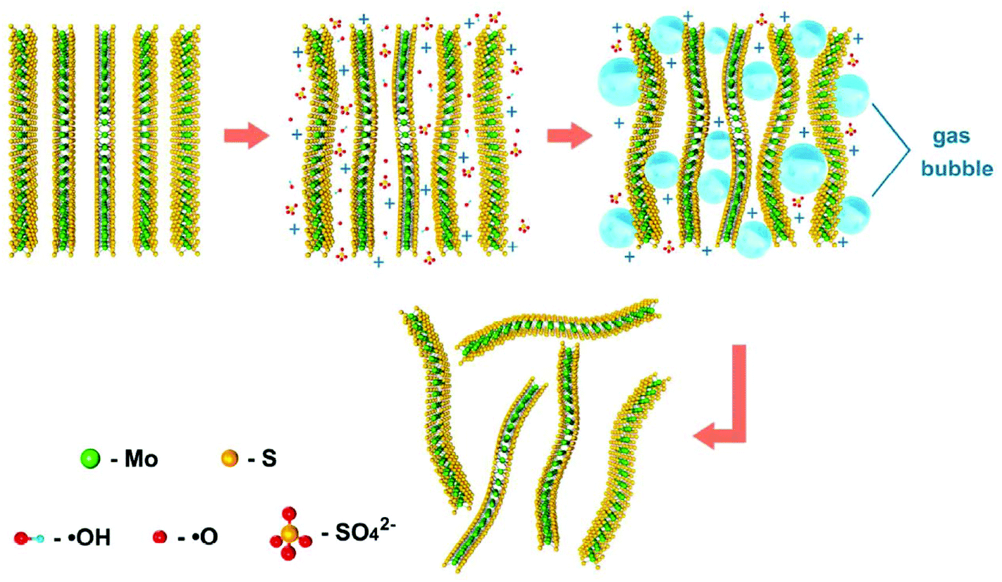 | ||
| Fig. 1 Schematic illustration for mechanism of electrochemical anodic exfoliation of bulk MoS2 crystals. Reproduced from ref. 44 with permission from the American Chemical Society, Copyright 2014. | ||
In contrast to anodic exfoliation, pristine 2D materials can be obtained via cathodic exfoliation as cathodic exfoliation of bulk layered materials is always carried out in an organic solution of alkali metal ions or quaternary ammonium cations under highly negative charge. Many factors, such as the size of the anions (Table 3),32,42,45 physical properties of solvents (Tables 1 and 2),26,42 bias voltage or current density (Tables 1 and 2),28,45 could affect the intercalating process significantly, as well as affecting the quality of the exfoliated 2D materials. In 2011, a mechanism of cathodic exfoliation of MoS2 (Fig. 2a) was proposed by Zeng et al. in an organic solution (a mixture of ethyl carbonate (EC) and dimethyl carbonate (DMC) in a volume ratio of 1![[thin space (1/6-em)]](https://www.rsc.org/images/entities/char_2009.gif) :1) of LiPF6.21 As a negative electric field was applied, the bulk MoS2 would be intercalated by Li+, as shown in step 1 in Fig. 2a. After completion of lithium insertion (step 2 in Fig. 2a), MoS2 was completely transformed into the intercalated compound LixMoS2. During this process, the interlayer distance would be expanded, and the van der Waals interactions between the layers would be weakened. Then, the intercalated compound LixMoS2 was ultrasonicated in water or ethanol to exfoliate and isolate 2D nanosheets (step 3 in Fig. 2a). The metallic Li formed during the insertion process would react with water, forming H2 gas, which pushes the layers further apart. In another example, Lin et al. utilized a large cation of tetraheptylammonium bromide (THA+, d ≈ 2.0 nm) in acetonitrile (AN) to insert into layers of MoS2 crystals, causing a substantial volume expansion of the MoS2 crystal.45 Recently, Yang et al. have investigated the exfoliation of black phosphorus (BP) in propylene carbonate (PC) solutions of various cations, such as Li+, Na+ and tetra-alkyl-ammonium (alkyl = methyl, ethyl or n-butyl) cations (termed TMA+, TEA+ or TBA+, respectively). They proved that BP can be hardly expanded in a solution of alkali ions with a small radius (e.g. Li+ 0.09 nm and Na+ 0.12 nm).42 Unlike alkali ions, quaternary ammonium cations generally exhibit large diameters (e.g. TMA+ 0.56 nm, TEA+ 0.67 nm, and TBA+ 0.83 nm), even greater than the interplanar spacing of BP (d = 0.53 nm). In the solution of tetra-n-butylammonium bisulfate (TBA·HSO4), a dramatic volume expansion could be observed within 15 min (Fig. 2b).42 For the quaternary ammonium cations with small diameters (e.g. TMA+ and TEA+), they showed a limited extent of expansion.42 In addition, the HSO4− anion in the electrolyte solution would generate solvated protons, and the solvated protons could give birth to hydrogen gas at the BP interfaces during the insertion process, resulting in the enlargement of the gaps between the neighboring layers, which could offer space for the intercalation of tetrahedral TBA+ cations with a maximum gallery expansion of 0.89 nm.42 At the same time, cathodic reduction could convert the TBA+ cations into various species (eqn (1)–(3)),46 which would further broaden the interlayer distance.42
:1) of LiPF6.21 As a negative electric field was applied, the bulk MoS2 would be intercalated by Li+, as shown in step 1 in Fig. 2a. After completion of lithium insertion (step 2 in Fig. 2a), MoS2 was completely transformed into the intercalated compound LixMoS2. During this process, the interlayer distance would be expanded, and the van der Waals interactions between the layers would be weakened. Then, the intercalated compound LixMoS2 was ultrasonicated in water or ethanol to exfoliate and isolate 2D nanosheets (step 3 in Fig. 2a). The metallic Li formed during the insertion process would react with water, forming H2 gas, which pushes the layers further apart. In another example, Lin et al. utilized a large cation of tetraheptylammonium bromide (THA+, d ≈ 2.0 nm) in acetonitrile (AN) to insert into layers of MoS2 crystals, causing a substantial volume expansion of the MoS2 crystal.45 Recently, Yang et al. have investigated the exfoliation of black phosphorus (BP) in propylene carbonate (PC) solutions of various cations, such as Li+, Na+ and tetra-alkyl-ammonium (alkyl = methyl, ethyl or n-butyl) cations (termed TMA+, TEA+ or TBA+, respectively). They proved that BP can be hardly expanded in a solution of alkali ions with a small radius (e.g. Li+ 0.09 nm and Na+ 0.12 nm).42 Unlike alkali ions, quaternary ammonium cations generally exhibit large diameters (e.g. TMA+ 0.56 nm, TEA+ 0.67 nm, and TBA+ 0.83 nm), even greater than the interplanar spacing of BP (d = 0.53 nm). In the solution of tetra-n-butylammonium bisulfate (TBA·HSO4), a dramatic volume expansion could be observed within 15 min (Fig. 2b).42 For the quaternary ammonium cations with small diameters (e.g. TMA+ and TEA+), they showed a limited extent of expansion.42 In addition, the HSO4− anion in the electrolyte solution would generate solvated protons, and the solvated protons could give birth to hydrogen gas at the BP interfaces during the insertion process, resulting in the enlargement of the gaps between the neighboring layers, which could offer space for the intercalation of tetrahedral TBA+ cations with a maximum gallery expansion of 0.89 nm.42 At the same time, cathodic reduction could convert the TBA+ cations into various species (eqn (1)–(3)),46 which would further broaden the interlayer distance.42
| (n-Bu)4N+ + e− → (n-Bu)4N | (1) |
| (n-Bu)4N˙ → n-Bu˙ + (n-Bu)3N | (2) |
| n-Bu˙ + e− → n-Bu− | (3) |
 | ||
| Fig. 2 Electrochemical lithiation process for the fabrication of 2D nanosheets from a layered bulk material (a). Reproduced from ref. 21 with permission from Wiley-VCH, Copyright 2011. Illustrative mechanism for the intercalation process of BP in a PC solution of TBA·HSO4 (b). Reproduced from ref. 42 with permission from Wiley-VCH, Copyright 2018. | ||
| Bulk layered materials | Interlayer distance (Å) | Ionic radius of the intercalants (Å) |
|---|---|---|
| BP | 5.4 (ref. 126) | Li+ (0.76), Na+ (1.02), TMA+ (5.6), TEA+ (6.7), TBA+ (8.3)42 |
| Sb | 3.8 (ref. 127) | Li+ (0.76), Na+ (1.02), K+ (1.38),128 Cs+ (1.69)129 |
| MoS2 | 6.1 (ref. 45) | THAB (20)45 |
| Ti3AlC2 | 9.3 (ref. 113) | 1.1 (OH−),130 1.8 (Cl−)34 |
3. Electrochemical exfoliation of 2D materials
3.1 Monoelemental Xenes
Many 2D monoelemental Xenes, including metallic group-IIIA (borophene) materials, semimetallic group-IVA (graphene, silicene, germanene and stanene) materials and group-VA (phosphorene, arsenene, antimonene and bismuthene) semiconductors, have been successfully synthesized in recent years and have emerged with increasing research interest in both fundamental and practical applications.8–10 Both two- and three-center B–B bonds can form in boron. The interactions between these bonding configurations result in more than 16 bulk allotropes of boron, composed of icosahedral B12 units, small interstitial clusters, and fused supericosahedra.47 Among them, β-B106 (rhombohedral) is the most stable phase under atmosphere pressure (1 atm).48 It was found that bulk β-B106 materials could not be exfoliated into borophene due to its structure. However, 2D monolayer or multilayer borophene sheets can be fabricated through physical methods like molecular beam epitaxy.47–49Despite intense theoretical investigations of the electronic and structural properties of group-IVA silicene and germanene, there are currently only a few experimental reports on silicene and germanene sheets, which is due to the inaccessibility of substrates and the crystal structure of the bulk materials.9 Currently, chemical vapor deposition, epitaxial growth and electrochemical deposition are the most common ways to obtain silicene and germanene.9,50,51 Very recently, an electrochemical lithiation and delithiation method (Fig. 3a) has been developed to fabricate few layer silicene nanosheets from ball-milled silicon nanopowders.29 By tuning the delithiation agent, silicene nanosheets of 30–100 nm length and ca. 2.4 nm thickness (Fig. 3b and c) can be obtained when silicon is fully lithiated. This is the first report on the electrochemical lithiation and delithiation exfoliation of nonlayered bulk materials into 2D Xenes materials. It is deduced that delithiation solvents play a critical role in the microstructure evolution of the final products as the proton concentration can determine the rate of delithiation. Taking deionized water as the delithiation solvent, a layered structure material resembling bulk graphite is obtained. In isopropyl alcohol, lithium is extracted slowly from fully lithiated Si nanopowders. This allows sufficient time for the newly formed surface to be functionalized, which can avoid restacking of the as-generated silicene nanosheets. As a result, few-layer silicene nanosheets can be successfully synthesized taking isopropyl alcohol as the delithiation solvent utilizing this method. However, the detailed mechanism of the structural transformation during the process of delithiation is still doubtful. It is worth looking for the mechanism of electrochemical exfoliation of nonlayered bulk materials.
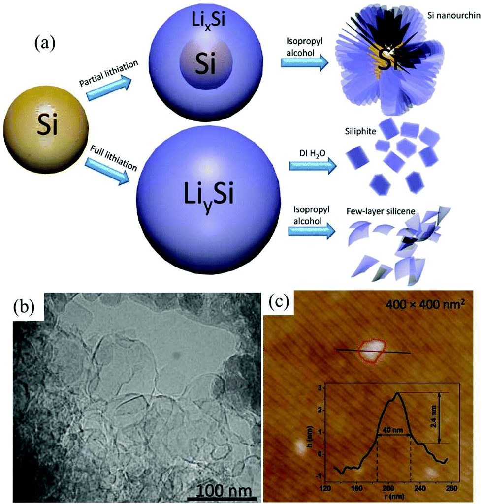 | ||
| Fig. 3 Scheme of lithiation and delithiation processes of silicon in different scenarios (a). TEM (b) and AFM (c) images of few layer silicene. Reproduced from ref. 29 with permission from Wiley-VCH, Copyright 2018. | ||
Bulk metallic β-tin with a tetragonal structure is stable at and above room temperature. In contrast, nonmetallic α-tin is stable below 13.2 °C. The α-tin has a diamond cubic crystal structure, similar to diamond, silicon or germanium. Stanene, a 2D allotrope of Sn in a graphene-like structure, is composed of a biatomic layer of α-tin(111), in which two triangular sublattices stack together, forming a buckled honeycomb lattice.52 Recently, 2D stanene films were successfully fabricated by Qian et al. through molecular beam epitaxy on the Bi2Te3(111) substrate.52 However, an exfoliation method taking stable β-tin or α-tin as the precursor has not been reported so far. In our previous studies, electrochemically cathodic exfoliation methods have been tried to fabricate 2D stanene in N,N-dimethylformamide (DMF) solutions of a quaternary ammonium salt and aqueous NaOH solutions utilizing a metallic β-tin electrode as the precursor; however, only Sn nanoparticles can be obtained.53,54 As can be seen, the cathodic exfoliation mechanism of metallic β-tin in these two solutions involves the formation of Zintl compounds like [(CH3)4N+]4Sn94− (Fig. 4a),54 intermetallic compound NaSn, and metal hydride SnH4 (Fig. 4c),53 and their simultaneous and/or subsequent decomposition, which can only cut the bulk tin into tiny Sn tetragonal nanoparticles (Fig. 4b and d), so no layered 2D stanene sheet can be obtained in these electrochemical exfoliation processes.
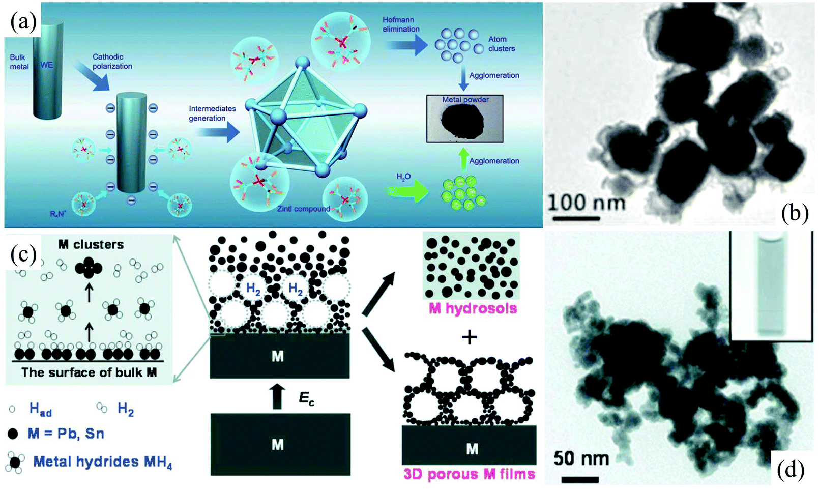 | ||
| Fig. 4 Schematic illustrations of the electrochemical exfoliation of Sn in DMF solution (a). The nanoparticles of tin were prepared through cathodic polarization of tin and lead electrodes, in situ generation of Zintl intermediates (R4N+)4M94− and their simultaneous and/or subsequent Hofmann elimination or oxidation by water at room temperature. TEM images of Sn nanoparticles prepared in a 0.1 M DMF solution of tetramethylammonium hexafluorophosphate (b). Reproduced from ref. 54 with permission from the Royal Society of Chemistry, Copyright 2015. Schematic illustration of the fabrication of Sn hydrosols under highly cathodic polarization in aqueous NaOH solution (c). TEM images (d) of Sn nanoparticles fabricated in aqueous NaOH solution. Reproduced from ref. 53 with permission from ECS, Copyright 2010. | ||
Group-VA phosphorus has four main allotropes (Fig. 5): white, red, black and violet. Among them, orthorhombic black phosphorus with its layered crystal structure is the most thermodynamically stable allotrope.55 Analogous to graphite in appearance, bulk black phosphorus made of puckered sheets of covalently bonded phosphorus atoms is flaky and shiny black and has good electrical conductance.56 It is also a layered material consisting of corrugated planes of phosphorus atoms with weak interlayer van der Waals interactions.57 As a result, it can be easily broken to obtain 2D single-layer black phosphorus called “phosphorene”. 2D phosphorene has many intriguing characteristics such as a tunable direct bandgap, high mobility, large on/off ratios (>105), anisotropic in-plane properties, and a high theoretical specific capacity (for sodium-ion batteries (SIBs), up to 2596 mA h g−1) and has attracted tremendous attention owing to its applications in photonics, electronics, optoelectronics, energy conversion and storage devices.55,58 To date, mechanical exfoliation, liquid phase exfoliation, plasma-assisted treatment, pulsed laser deposition, electrochemical exfoliation, and chemical vapor deposition methods have been adopted to fabricate 2D phosphorene. Among them, electrochemical exfoliation is considered a simple, green, and controllable method. Both electrochemical anodic exfoliation and cathodic exfoliation can be utilized to obtain 2D phosphorene. Two-step anodic exfoliation was first utilized by Pumera et al. in 2017 to reduce the thickness of bulk black phosphorus in an aqueous H2SO4 solution.27 As shown in Fig. 6a, bulk black phosphorus flakes and Pt foils were used as the anode (electrically connected through Cu tape) and cathode, respectively. During the initial stage, a positive DC voltage of 1 V was applied to the black phosphorus crystals for 2 min to facilitate wetting. Then, the voltage was increased to +3 V, resulting in the intercalation of anionic SO42−, the expansion of the interlayer and the exfoliation of phosphorene.24 The products phosphorene nanosheets characterized by STEM (Fig. 6b and c) show a reduced thickness. In their X-ray photoelectron spectroscopy results shown in Fig. 6d and e, the electrochemically exfoliated phosphorene nanosheets are dominated by the oxide contribution. Analogous to anodic exfoliation of graphite, exfoliated nanosheets are more prone to oxidation, which can also be favored by the anodic exfoliation process itself. In contrast with anodic exfoliation, cathodic exfoliation of black phosphorus was always carried out utilizing bulk black phosphorus as the cathode, which can avoid electrochemical oxidation of the final exfoliated products. As a result, phosphorene nanosheets with low oxidation degrees can be obtained. For instance, electrochemical cathodic exfoliation of black phosphorus in a DMF solution of a quaternary ammonium salt (Fig. 7a) was developed by Ji et al. to fabricate large-area low oxygen-contained phosphorene, in which tetrabutylammonium cations (TBA+) were triggered to be inserted into the interlayers of black phosphorus and the weak interlayer van der Waals interactions were broken under a constant applied voltage, resulting in the expansion, curling, stripping and peeling of black phosphorus.28 The number of phosphorene layers could be tuned by the cation insertion rate through changing the applied potential. Recently, Jia et al. also proved that few-layer phosphorene nanosheets can be fabricated through electrochemical cathode exfoliation of bulky black phosphorus in a PC solution of TBA+ with a large size of its cation under highly negative charge (Fig. 7b).25 At the same time, Li et al. also developed an ultrafast cathodic process employing TBA+ as the cationic intercalant (Fig. 7c) but in the presence of polar organic aprotic solvent to exfoliate bulk black phosphorus.26 Dimethyl sulfoxide (DMSO), with high dispersion capability of black phosphorus and strong donicity, was chosen as the organic electrolyte. Through applying a voltage of −5 V to the black phosphorus cathode, fast expansion and exfoliation (below 1 min) resulted in large quantities of high-quality and solution-processable few-layer phosphorene with negligible structural deterioration, excellent electronic properties, great solution processability, and high air stability. To improve the exfoliation yield and quality of phosphorene, Yang et al. developed an efficient and scalable delamination method utilizing tetra-n-butylammonium bisulfate (TBA·HSO4) as the intercalating agent.42 Besides the intercalation of TBA+, the penetration and reduction of solvated protons (HSO4− ⇌ SO42− + H+, 2H+ + 2e− → H2) would also assist the exfoliation process, resulting in a high exfoliation yield up to 78% and a large lateral dimension of exfoliated few-layer oxygen-free phosphorene flakes (up to 20.6 mm).42 Nevertheless, the fabrication of monolayer phosphorene through electrochemical exfoliation is still challenging. More appropriate solvent, electrolyte or electrochemical parameters need to be further optimized.
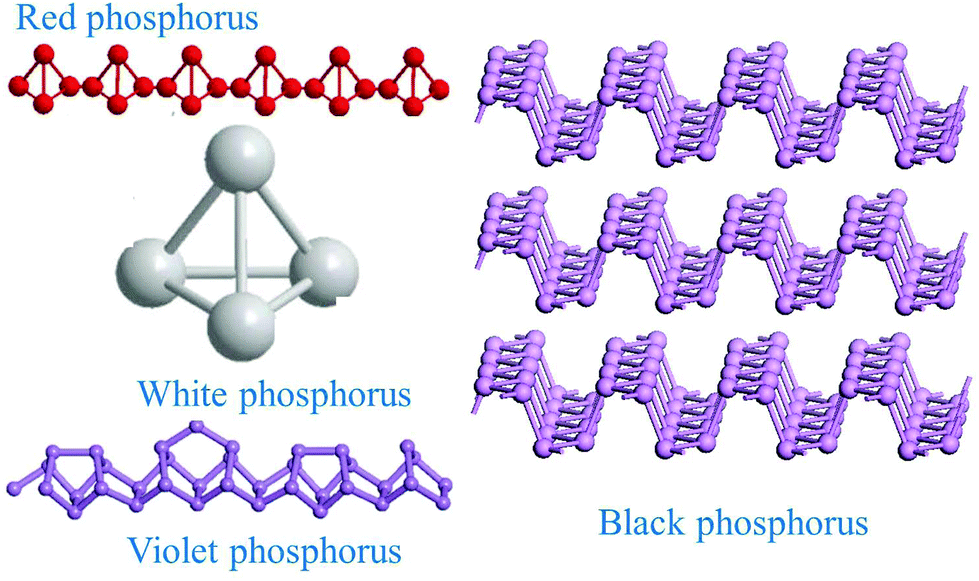 | ||
| Fig. 5 Main allotropes of phosphorus. Reproduced from ref. 55 with permission from Wiley-VCH, copyright 2017. | ||
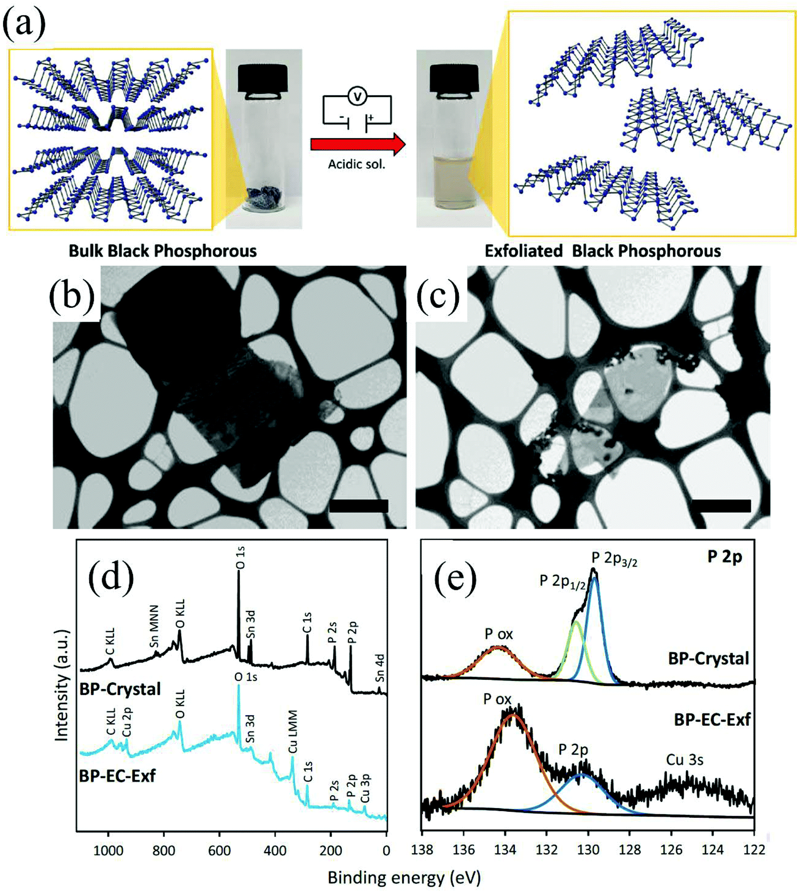 | ||
| Fig. 6 Schematic diagram of the exfoliation procedure (a). Layered crystal structure of black phosphorus is exfoliated in acidic aqueous solution by the application of a DC voltage. Pictures of the starting BP crystals (left) and the exfoliated material dispersion in DMF (right) are also shown. Scanning transmission electron microscopy images of the bulk crystal of black phosphorus (b) and exfoliated black phosphorus nanosheet (c). Scale bar corresponds to 1 μm. XPS survey spectra (d) of crystal BP (black) and electrochemically exfoliated BP. High-resolution XPS spectra (e) of the P 2p signal for the crystal BP (upper) and electrochemically exfoliated BP (lower). Reproduced from ref. 27 with permission from Wiley-VCH, Copyright 2017. | ||
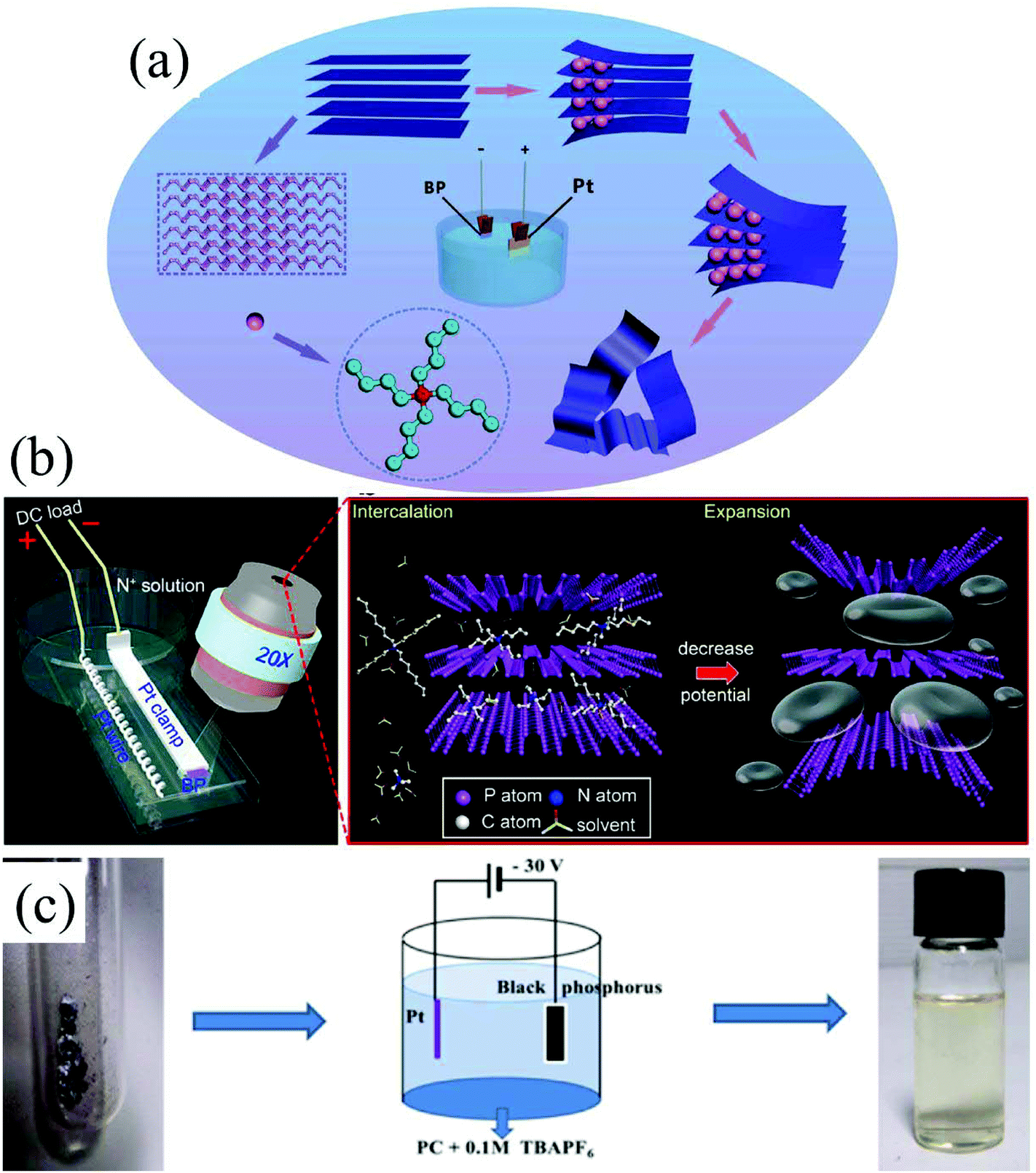 | ||
| Fig. 7 Schematic illustration of the electrochemically cathodic exfoliation of bulky BP in DMF (a), PC (b) and DMSO (c) solutions of TBA+. (a) Reproduced from ref. 28 with permission from Wiley-VCH, Copyright 2017. (b) Reproduced from ref. 26 with permission from the American Chemical Society, Copyright 2018. (c) Reproduced from ref. 25 with permission from Elsevier, Copyright 2018, respectively. | ||
The heavy pnictogens (As, Sb, and Bi) crystallize with a rhombohedral layered structure, which is the most stable allotropic form of these elements.7 This rhombohedral structure is similar to the structure of black phosphorus consisting of puckered, six-membered rings of atoms; nevertheless, individual layers are held together by much stronger interactions.7 Due to the interaction of atomic orbitals between the individual double layers, these bulk materials (As, Sb, Bi) do not form true van der Waals bonded layered materials. Accordingly, these bulk materials made up of As, Sb or Bi element, with rhombohedral layered structures, are extremely fragile and can be easily powdered, which makes it easy to exfoliate them into single- or few-layer 2D materials by mechanical, sonochemical, liquid phase, or shear exfoliation.59–62 Recently, a facile and environmentally friendly electrochemical exfoliation method has also been developed to design 2D antimonene.30,31 The exfoliation process was carried out in 0.2 M aqueous Na2SO4 solution utilizing bulk layered Sb as the cathode under a constant voltage of −6 V.30 After exfoliation for 60 min, multilayer rhombohedral antimonene with a thickness of 31.6 nm can be obtained. When stored under ambient conditions for 25 days, no obvious change has been found, indicating the relative stability of this multilayer rhombohedral antimonene. Moreover, this electrochemically exfoliated antimonene, with a nonlinear refractive index similar to BP, shows higher stability than black phosphorus, suggesting that antimonene can be considered as a potential candidate for optical switching and optical communication applications.30 In the results of MacFarlane et al., a more concentrated aqueous solution of 0.5 M Na2SO4 was used as the electrolyte solution, and a more negative voltage of −10 V was applied, resulting in the formation of large 2D few-layer rhombohedral antimonene nanosheets with an average thickness down to 3.5 nm.31 It is found that the anion of the supporting electrolyte has little influence on the exfoliation process, while cations with either too large (i.e., Cs+) or too small (i.e., Li+) sizes compared to the interplanar spacing of Sb crystals decrease the exfoliation rate. However, the mechanism for electrochemical exfoliation of layered Sb is still unclear, as the cathodic exfoliation process of layered Sb crystals in aqueous solution is quite different from that of graphite. During the cathodic exfoliation of graphite in an organic solution of lithium salts or quaternary ammonium salt, the cations (i.e., Li+) can intercalate into graphite layers, resulting in the formation of graphite intercalation compounds and the weakening of the van der Waals interactions between the layers, which will lead to the expansion of the interlayer and the exfoliation of graphite into graphene.23,63,64 However, the plane structure would not be destroyed since the covalent bond in the intralayer of the 2D graphene plane is much stronger than that of the interlayer interactions. As for cathodic exfoliation of layered Sb in aqueous solution, the intermediate amorphous phase NaxSb, cubic–hexagonal Na3Sb mixture phases, and volatile unstable stibine (antimony hydride, SbH3) will be formed firstly around the cathode during the intercalation of Na+ cations under highly negative charge.65–69 Consequently, the original layered structure of crystalline Sb will be destroyed during the first intercalation. Then, the reactive intermediates NaxSb, Na3Sb, and SbH3 will react with H2O or decompose spontaneously, resulting in the formation of low-dimensional metallic Sb nanomaterials.69,70 However, the mechanism of the chemical reaction of the intermetallic compounds with H2O and the decomposition of SbH3 is still doubtful. Further theoretical and experimental studies should be carried out to investigate the crystal transformation process in future, which will help us to finally understand the mechanism of electrochemically cathodic exfoliation of layered Sb into 2D antimonene.
3.2 Transition-metal dichalcogenides
Transition-metal dichalcogenides (TMDs) show a wide range of chemical, thermal, electronic, optical, and mechanical properties that have been extensively studied and applied in catalysis, energy storage, photovoltaics, lubrication, electronics, and optoelectronics.9,71–76 Structurally analogous to graphene, TMD bulk crystals are layered structures with strong covalent bonding in each layer and weak van der Waals forces between the layers.21 As a result, their bulky forms can be easily exfoliated along these planes because of the weak interlayer interactions. Like graphite, micromechanical cleavage is considered the best method for exfoliating layered TMD crystals with a view to investigating their inherent physical properties.44,77,78 However, this method is very inefficient, and it is difficult to control the flake thickness and the size of the products. Chemical vapor deposition (CVD) can be used to obtain monolayer TMDs, but the requirement for sophisticated equipment makes it challenging for scale-up.79–82 For obtaining large quantities of single-layer and multilayered TMD nanosheets, solution-based exfoliation is very promising.83–85 So far, intriguing solution-based electrochemical exfoliation methods such as anodic exfoliation44,86 and cathodic exfoliation have also been adopted to design 2D TMD nanosheets.32,44The electrochemical lithium intercalation cathodic exfoliation of bulk layered TMD crystals was established by Zeng et al. in 2011.21 In their experiment set-up, lithium metal foils and TMD crystals were used as the anode and the cathode (Fig. 2a), respectively. When discharging at constant current, lithium ions are intercalated into the interlayer spaces of the bulk layered TMD crystals and the intercalated compounds (e.g. LixMoS2) are formed. At the same time, the interlayer distance is expanded, which can weaken the van der Waals interactions between the layers. After that, the intercalated compounds washed with acetone are ultrasonicated in water or ethanol to exfoliate and separate the 2D nanosheets. During this, the intercalated lithium in the intercalated compounds formed during the discharge process reacts with water or ethanol to generate H2 gas, which pushes the layers further apart, resulting in the final exfoliation of single-layer 2D nanosheets. This electrochemical lithium intercalation method was first established for MoS2, WS2, TiS2, TaS2, ZrS2 and graphene (Fig. 8a–d),21 and then for BN, NbSe2, WSe2, Sb2Se3 and Bi2Te3.87 Although this method can exfoliate layered compounds into monolayers (e.g. single-layer MoS2), it is difficult to eliminate the doping effect created by the residual lithium, which will lead to the loss of the 2D MoS2 nanosheets’ semiconducting properties.88,89
 | ||
| Fig. 8 TEM image, SAED pattern and HRTEM image (a) of a single-layer MoS2 nanosheet. Inset: photograph of a MoS2 solution. TEM image, SAED pattern and HRTEM image (b) of a single-layer WS2 nanosheet. Inset: photograph of a WS2 solution. TEM image, SAED pattern and HRTEM image (c) of a single-layer TiS2 nanosheet. Inset: photograph of a TiS2 solution. TEM image, SAED pattern and HRTEM image (d) of a single-layer TaS2 nanosheet. Inset: photograph of a TaS2 solution. Reproduced from ref. 21 with permission from Wiley-VCH, Copyright 2011. | ||
To obtain high-quality thin MoS2 nanosheets, electrochemical anodic exfoliation of bulk MoS2 crystals was carried out by Liu et al. in 2014.44 As shown in Fig. 9a–d, a bulk layered MoS2 crystal, a Pt wire, and a 0.5 M aqueous Na2SO4 solution were used as the anode, the counter electrode, and the electrolyte, respectively. The exfoliated monolayer and few-layer MoS2 nanosheets with lateral size as large as 50 μm exhibit high quality and an intrinsic structure (Fig. 9e and f). However, the surface of the exfoliated 2D MoS2 nanosheets can be easily oxidized (Fig. 9g) during the electrochemical anodic exfoliation, which will reduce the quality of the exfoliated 2D materials. Similar to cathodic exfoliation of non-oxidative phosphorene, defect-free non-oxidative MoS2 nanosheets with a lateral size of tens of micrometers can also be obtained by cathodic exfoliation of a natural bulk MoS2 crystal in an acetonitrile solution of TBA+ utilizing a two-compartment electrochemical cell (the anode is graphite).32 When the two-compartment electrochemical cell was replaced by a single-compartment cell, a MoS2-graphene composite can be produced in situ using micro-scale MoS2 powder mixed graphite (25 wt%) as the cathode. The TEM results exhibit the MoS2 basal plane overlapping and stacking with the basal plane of graphene, which promotes fast charge transfer between the MoS2 nanosheets and the substrate electrode. As a result, the electrochemically exfoliated MoS2 nanosheet–graphene composite shows superior electrocatalytic activity towards hydrogen evolution reaction (HER), in comparison with MoS2 nanosheets or bulk MoS2 powder. Furthermore, these cathodic exfoliation methods can be extended to exfoliate other layered materials such as layered birnessite-type δ-MnO2 and graphitic carbon nitride.32 Very recently, Lin et al. utilized a large cation of tetraheptylammonium bromide ((C7H15)4NBr, d ≈ 2.0 nm) in acetonitrile (AN) to exfoliate MoS2 crystals under a cathodic potential.45 After the intercalation of the (C7H15)4NBr molecules, the interlayer spacing of MoS2 was expanded from the original 6.1 Å to 22.9 Å. By precisely controlling the intercalation chemistry and the sonication dispersion, phase-pure, semiconducting 2H-MoS2 nanosheets with a thickness distribution of 3.8 ± 0.9 nm and lateral dimensions of 0.5–2 μm were successfully fabricated.
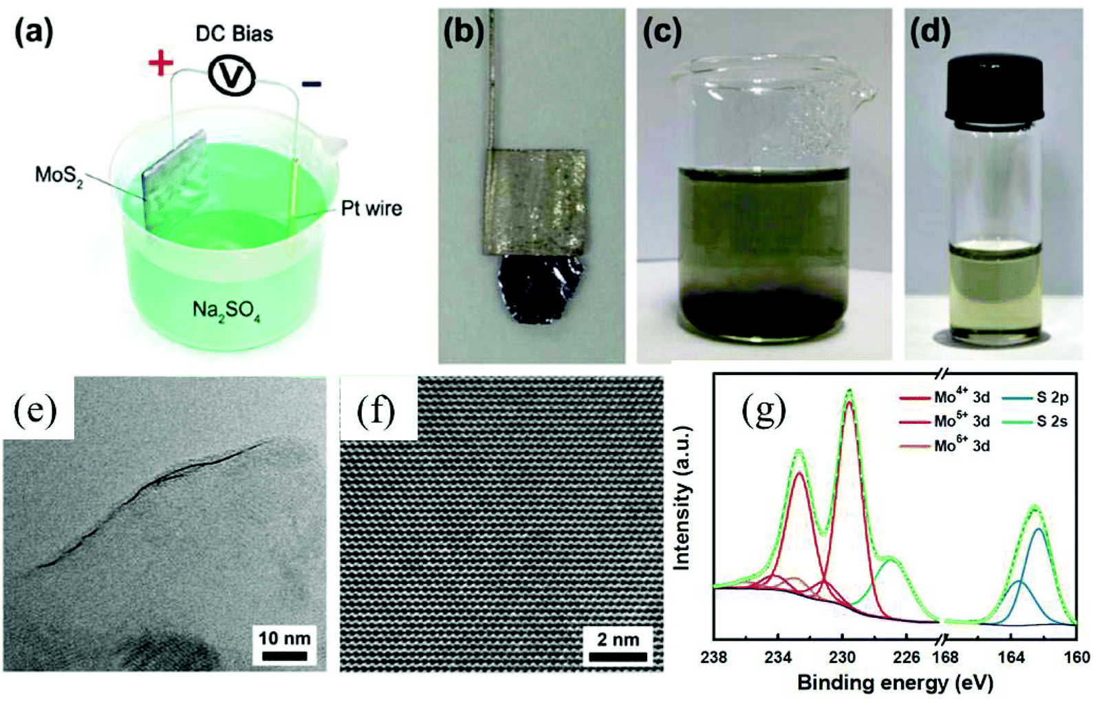 | ||
| Fig. 9 Schematic illustration of the experimental setup for electrochemical exfoliation of a bulk MoS2 crystal (a). Photograph of a bulk MoS2 crystal held by a Pt clamp before exfoliation (b). Exfoliated MoS2 flakes suspended in Na2SO4 solution (c). MoS2 nanosheets dispersed in NMP solution (d). HRTEM image of a monolayer MoS2 nanosheet showing a layer edge (e). HRTEM image of a hexagonal lattice structure of a MoS2 nanosheet (f). XPS characterization of an as-prepared MoS2 nanosheet (g). Reproduced from ref. 44 with permission from the American Chemical Society, Copyright 2014. | ||
For 2D ultra-thin MoS2 nanosheets, when confined to zero dimension (0D), the quantum size effects and the edge effects become very significant,90,91 resulting in some interesting physical and chemical properties.92,93 The electrochemical method is still one of the most powerful tools to cut down the bulk MoS2 into ultra-small MoS2 quantum dots. Zhong et al. developed a multi-exfoliation method based on lithium intercalation (Fig. 10a) to fabricate monolayer MoS2 quantum dots (QDS) from bulk MoS2 powder.94 The cutting mechanism of bulk MoS2 powder into QDs involves the complete breakup around the defects and edges during the reaction of LixMoS2 with water and its following ultrasonication process. The exfoliated monolayer MoS2 QDs shown in Fig. 10e with a lateral size of around 3 nm (Fig. 10b–d) photoluminescence (PL) was inactive due to the existence of 1 T phase. After ultrasonicated heating treatment (Fig. 10f), the PL intensity excited at 300 nm significantly increases. The luminescent QDs of MoS2 (≤2 layers) with a narrow size distribution, ranging from 2.5 to 6 nm, are also electrochemically exfoliated from bulk MoS2 material by Shaijumon et al. in aqueous ionic liquid solutions of 1-butyl-3-methylimidazolium chloride ([BMIm]Cl) and lithium bis-trifluoromethylsulphonylimide (LiTFSI) under a constant DC potential.93 During the first stage, the exotic hydroxyl and oxygen free radicals formed near the surface of the bulk MoS2 anode trigger the initial cleavage of the bulk layered material. As time progresses, the MoS2 anode is expanded by the incorporation of TFSI− and Cl3− anions, respectively, in LiTFSI and [BMIm]Cl based electrolytes and MoS2 QDs start dissolving in the electrolyte.
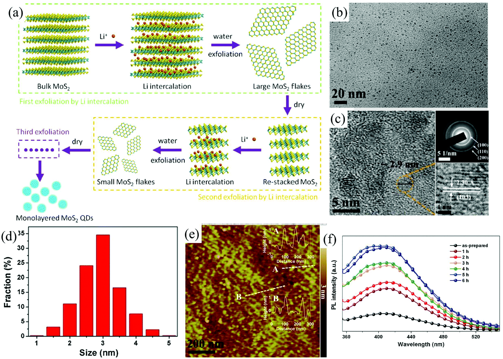 | ||
| Fig. 10 Schematic illustration of the preparation of monolayer MoS2 QDs using multiple exfoliations with Li intercalation (a). TEM images (b), HRTEM image and SAED pattern (c), size distribution (d), and AFM image (e) of monolayer MoS2 QDs. PL spectra (f) of the monolayer MoS2 QD solution before and after ultrasonicated heating treatment at different hours. Reproduced from ref. 94 with permission from Elsevier, copyright 2015. | ||
3.3 Metal–organic framework (MOF) nanosheets
Metal–organic framework (MOF) materials, also known as porous coordination polymers (PCPs), are composed of transition-metal ions linked together by organic bridging ligands.95–98 The transition-metal ions and organic ligands in MOFs are connected by coordination bonds and even weaker supramolecular interactions.33,99 Due to their large internal surface areas, ultralow densities, and diversified and designable structures, MOFs have attracted tremendous attention owing to their application in various fields such as methane and hydrogen storage, capture of carbon dioxide, chemical separation, and heterogeneous catalysis.100,101 2D MOF nanosheets, an important member of the 2D family, have many highly active sites on their surface, which make them significant for catalytic, electrochemical, and sensing applications.102 However, the intralayer bonds (coordination bonds) of MOFs are relatively weak and the interlayer interactions (hydrogen bonds, multiple interactions between the wrinkle surface, etc.) in bulk MOFs are relatively strong,10,103 which make it challenging to exfoliate bulk MOFs into 2D MOF nanosheets. The solution-based exfoliation of bulk MOFs reported recently is not feasible for the uniform and high-yield preparation of 2D MOF (normally the obtained yield of <15%), and the obtained nanosheets are not stable due to their restacking.104–106 Very recently, Huang et al. have developed an electrochemical/chemical exfoliation strategy to synthesize 2D MOF materials based on coordination bonds.33 Firstly, a novel 3D pillared-layer MOF ((H3O)2[Co6O(dhbdc)2(H2dhbdc)2(EtOH)4]2·EtOH) was synthesized utilizing a catechol functionalized ligand as the redox active pillar (Fig. 11a). Then, the as-synthesized 3D pillared-layer MOF (Fig. 11b–d) was used as an electrocatalyst for water oxidation. During the electrocatalysis process, the pillar ligands in MOFs can be in situ oxidized and removed, resulting in the formation of ultrathin (2 nm) 2D MOF layers (Fig. 11e–i). This in situ fabricated ultrathin 2D MOF shows exceptionally high OER activities.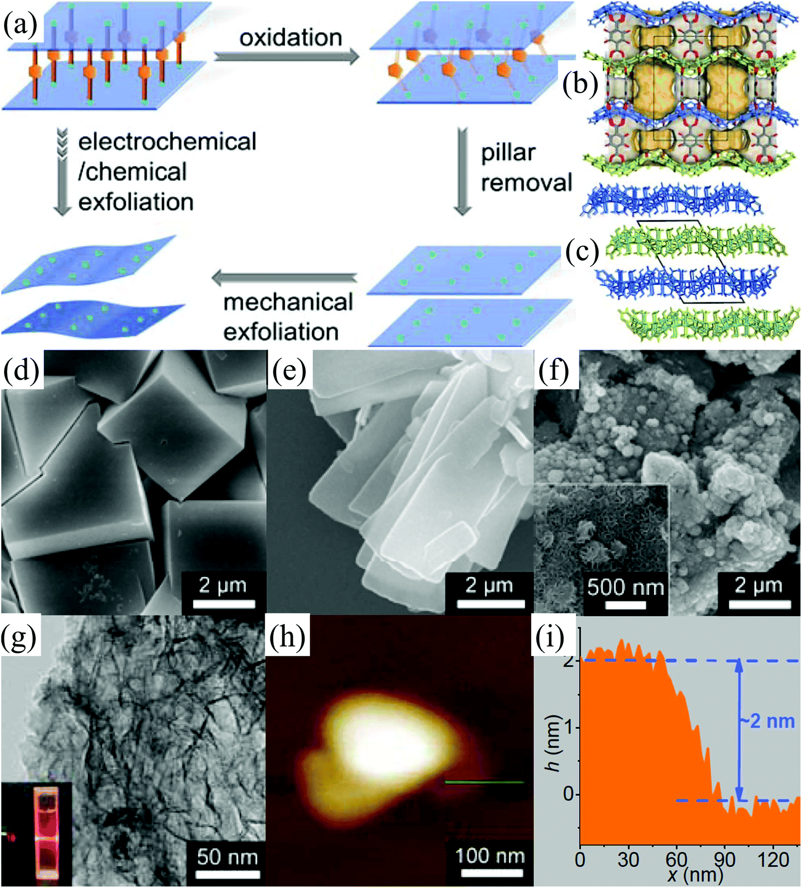 | ||
| Fig. 11 Selective pillar removal and exfoliation of a pillared-layer MOF (a). 3D pillared-layer structure (b) viewed along the a-axis with the pore surface highlighted in 3D-Co. 3D packing structure of the 2D layers (c) viewed along the b-axis in 2D-Co. SEM images of 3D-Co (d), 2D-Co (e) and 2D-Co-NS (f). A TEM image (g) of 2D-Co-NS (inset: the Tyndall effect of a colloidal solution). An AFM image (h) and (i) the corresponding height profile of 2D-Co-NS. Reproduced from ref. 33 with permission from Wiley-VCH, Copyright 2018. | ||
Mass spectroscopy of the acid-digested catalyst and the electrolyte solution was further carried out to study this electrochemical exfoliation mechanism. After electrolysis, a new species (m/z (M + H) = 169) corresponding to 2-oxocyclopenta-3,5-diene-1,3-dicarboxylic acid was found in the electrolyte solution. Compared with the original linear dicarboxylate ligand, the oxidation product possesses a bent bridging angle, and the electron donating hydroxyl groups are also replaced by electron withdrawing carbonyl groups. Consequently, they deduced that oxidized pillars with less suitable bridging angle and weaker coordination ability would have a higher tendency to leave the layers, which would lead to the exfoliation of bulk pillared-layer MOFs into 2D MOF nanosheets.
3.4 MXene
Due to their unique properties such as a large interlayer spacing, tunable structure, hydrophilic nature, high electrical conductivity, outstanding thermal stability, and high surface area, MXenes, including transition metal carbides, nitrides, and carbonitrides, have been emerging as two-dimensional materials for various applications beyond graphene.107–110 In general, these fascinating 2D materials are fabricated by selective etching of bulk 3D MAX phases. The MAX phase corresponds to the general formula Mn+1AXn (n = 1, 2, 3) where M is an early d-block transition metal (e.g., Sc, Ti, V, Cr, etc.), A represents main group sp elements (IIIA or IVA) and X stands for carbon and/or nitrogen.110,111 All known MAX phases are layered, hexagonal structures with P63/mmc symmetry, in which M layers are nearly hexagonally close-packed together, the X atoms fill the octahedral sites, and the element A is metallically bonded to the M element and interleaved in the Mn+1Xn layers.110 The M–X bond has strong covalent/metallic/ionic character whereas the bonding between M and A is a weak metallic bond.110 In contrast to weak van der Waals interactions between the layers of graphite or TMDs, the bonds between the MX layers in MAX phases are partial ionic bonds, which makes them difficult to be destroyed.112 Traditional physical methods, such as mechanical exfoliation and ultrasonication, can hardly exfoliate the 3D MAX phases into 2D MXenes. Luckily, the M–A bonds are weaker than the M–X bonds, the A layers can be selectively etched by suitable chemicals without destroying MX layers.110 The common chemicals used to exfoliate the MAX phases include hydrofluoric acid (HF) or fluoride-based compounds (LiF/HCl, NaHF2, KHF2 and NH4HF2).113–115 All the known chemicals are hazardous and they will greatly affect the surface functionalization, quality, and thickness of MXene flakes. Very recently, a fluoride-free electrochemical etching method (Fig. 12a) based on the anodic corrosion of titanium aluminium carbide (Ti3AlC2) has been developed by Yang et al. to synthesise 2D titanium carbide (Ti3C2).34 The electrolyte used here consists of 1 M NH4Cl and 0.2 M tetramethylammonium hydroxide (TMA·OH). In this method, the chloride ions in the electrolyte solutions can quickly etch Al and break the Ti–Al bonds under anodic potential (Ti3AlC2 – 3 e− + 3 Cl− = Ti3C2 + AlCl3).34 The subsequent intercalation of ammonium hydroxide (NH4OH) can open the edges of the etched anode and assist in etching the underlying surfaces. More than 90% of the exfoliated 2D carbide flakes (Ti3C2Tx, T = O, OH) are monolayers (Fig. 12e–g) with an average lateral size of over 2 μm (Fig. 12b–d), which is larger than the sizes achieved by classic HF etching methods.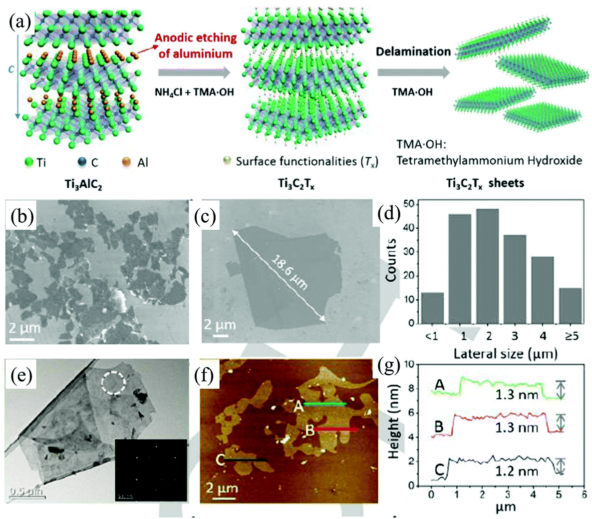 | ||
| Fig. 12 Schematic diagram of the etching and delamination process of bulk Ti3AlC2 in a binary aqueous electrolyte (a). SEM images (b), the corresponding statistical size distribution (c), TEM image (d), AFM image (e) and the relevant height profiles (f) of the delaminated Ti3C2Tx. Reproduced from ref. 34 with permission from Wiley-VCH, Copyright 2018. | ||
4. Potential applications
As reviewed above, 2D materials like phosphorene, antimonene, TMDs, MOFs, and MXenes can be fabricated through electrochemical exfoliation. By adjusting the electrochemical parameters (voltage/current), electrolyte and/or solvent, the properties of the products such the oxygen content, electrical conductivity, defect density and the thickness can be tuned to meet the demands of various applications.To overcome environmental pollution and gradual depletion of oil resources, energy storage systems have the potential to become key technologies. Among these candidates, lithium-ion batteries (LIBs) are the backbone of power sources for a wide range of applications, from portable electronic devices to increasing numbers of electric vehicles and large-scale energy storage devices.116,117 Cheaper sodium-ion batteries and supercapacitors with higher power density are now considered to be the most powerful candidates for next generation energy storage devices.118,119 All of these devices require the state-of-the-art materials. The electrochemically exfoliated phosphorene was studied as an anode material for SIB by Huang et al.28 Due to its large surface area and free surface functional groups, this few-layer phosphorene exhibits a high capacity of 1968 mA h g−1 at a current density of 100 mA g−1.28 Recently, 2D MXene carbide flakes (Ti3C2Tx, T = O, OH) with an average lateral size of over 2 μm were fabricated by Yang et al. through anodic corrosion of titanium aluminum carbide (Ti3AlC2) in a fluoride-free binary aqueous electrolyte.34 When used as an electrode material for an all-solid-state supercapacitor, it shows high areal and volumetric capacitances of 220 mF cm−2 and 439 F cm−3, superior to those of LiF/HCl-etched MXenes, which is due to the oxygen-rich surface groups (i.e. O or OH) that contribute to the pseudocapacitance with H+.34
In addition to their energy storage applications, one of the most important applications of exfoliated 2D materials is the field-effect transistor (FET), which is the indispensable building block of modern integrated circuits.8 Recently, Li et al. developed a rapid cathodic exfoliation method in a DMSO solution of TBA+ to exfoliate the bulk BP.26 Due to their low density of defects and low degree of surface oxidation, exfoliated phosphorene flake FET devices display a high mean hole mobility of ∼60 cm2 V−1 s−1 (up to ∼100 cm2 V−1 s−1) and a high on/off ratio (∼1 × 10⁴ on average).26 These results are better than that of BP thin flakes fabricated through other solution-phase exfoliation methods.120,121 Furthermore, the exfoliated phosphorene exhibits excellent dispersibility in alcohol and water, which makes it particularly attractive for the preparation of functional inks for large-area inkjet printing and for the fabrication of optoelectronic devices.26 Taking TBA·HSO4 as the intercalating agent, oxygen-free phosphorene flakes of up to 20.6 mm were synthesized by Yang et al.42 When used for bottom-gate and bottom contact FETs, they exhibit a high hole mobility of 252 ± 18 cm2 V−1 s−1 with an amazing on/off ratio of (1.2 ± 0.15) × 105 at 143 K under vacuum, which is the best carrier mobility reported to date for solution-processed BP flakes.42 Besides phosphorene, the electrochemically exfoliated 2D MoS2 is also an excellent semiconductor for FETs. For example, a thin-film transistor processed with highly uniform, solution-processable, phase-pure semiconducting 2H-MoS2 nanosheets fabricated through cathodic exfoliation in a solution of (C7H15)4NBr shows a room-temperature mobility of about 10 cm2 V−1 s−1 and an on/off ratio of 106,45 which greatly surpass the values obtained for previous lithium intercalation-exfoliated (mobility of ca. 0.3 cm2 V−1 s−1 and an on/off ratio of less than 10)21,122 and solution-processed MoS2 (mobility of ca. 0.4 cm2 V−1 s−1 and an on/off ratio of ca. 100) thin-film transistors.83,123,124
Apart from energy storage and FET device applications, electrochemically exfoliated 2D materials can also find application in catalysis and photonics devices.30–33,93 In 2015, Shaijumon et al. fabricated luminescent QDs of MoS2 (≤2 layers) through electrochemical exfoliation of bulk MoS2 in aqueous ionic liquid solutions of 1-butyl-3-methylimidazolium chloride ([BMIm]Cl) and lithium bis-trifluoromethylsulphonylimide (LiTFSI).93 The as-exfoliated MoS2 QDs showed excitation dependent luminescence and excellent HER activity. Few-layer antimonene, designed by Lu et al. with a cathodic exfoliation process in 0.2 M aqueous Na2SO4 solution under a constant voltage of −6 V, exhibits a giant nonlinear refractive index of ≈10−5 cm2 W−1 and a high stability under ambient conditions for months.30 These findings are considered an important step toward antimonene-based nonlinear photonics devices such as optical switchers, kerr shutters, beam shapers, and so on.125
5. Conclusion and prospects
Most of the bulk layered materials have strong in-plane bonds but weak interlayer bonding like van der Waals forces or electrostatic interactions. Electrochemical exfoliations such as anodic exfoliation and cathodic exfoliation can destroy or weaken the van der Waals forces or electrostatic interactions that bind 2D layers, which can be utilized to exfoliate the bulk layered materials into single-layer or few-layer 2D materials beyond graphene (Table 1). For those bulk layered materials which are semiconductive or nonconductive, they are difficult to be directly electrochemically exfoliated since most of the applied potential will be used to get over the huge resistance. To tackle this problem, inclusion of the conducting additive is an efficient strategy, which can make the exfoliation of an extensive range of layered materials possible regardless of the conductivity of the bulk materials. Through regulating the voltage, the electrolyte, the solvent, and even the shape of the original bulk materials, the structure and chemical and physical properties of the as-resulted 2D materials can be controlled. Also, the post-treatment after electrochemical exfoliation such as ultrasonication and delithiation will affect the quality of the final products. In comparison with other fabrication methods, electrochemical exfoliation is more convenient and controllable. However, the fabrication of most of the monolayer 2D materials through electrochemical exfoliation of bulk materials is still challenging. It is seen that most of the electrochemical exfoliation processes of bulk layered materials are carried out under unconventional electrochemical conditions, which makes it difficult to monitor the process of electrochemical exfoliation due to the intensive oxygen and hydrogen evolution stimulated by electrochemical polarization. Therefore, more efforts are needed to investigate the mechanism of the electrochemical exfoliation, which will promote the development of advanced two-dimensional materials with broad application prospects in the field of electronics, energy storage, energy conversions, sensors, corrosion prevention and catalysis in turn.Conflicts of interest
There are no conflicts to declare.Acknowledgements
Financial support from the National Natural Science Foundation of China (21805211, 51862033, 51622406, and 21673298), National Key Research and Development Program of China (2017YFB0102003 and 2018YFB0104204), Department of Education of Guizhou Province (No. KY[2016]106) and Department of Science and Technology of Guizhou Province (QKH[2017]1185 and QKH[2018]1164), and Innovation Mover Program of Central South University (2017CX004, 2018CX005) is greatly appreciated.References
- K. S. Novoselov, A. K. Geim, S. V. Morozov, D. Jiang, Y. Zhang, S. V. Dubonos, I. V. Grigorieva and A. A. Firsov, Science, 2004, 306, 666–669 CrossRef CAS PubMed.
- M. J. Allen, V. C. Tung and R. B. Kaner, Chem. Rev., 2010, 110, 132–145 CrossRef CAS PubMed.
- V. Singh, D. Joung, L. Zhai, S. Das, S. I. Khondaker and S. Seal, Prog. Mater. Sci., 2011, 56, 1178–1271 CrossRef CAS.
- W. Choi, I. Lahiri, R. Seelaboyina and Y. S. Kang, Crit. Rev. Solid State Mater. Sci., 2010, 35, 52–71 CrossRef CAS.
- S. Balendhran, S. Walia, H. Nili, S. Sriram and M. Bhaskaran, Small, 2014, 11, 640–652 CrossRef PubMed.
- S. Rachel and M. Ezawa, Phys. Rev. B: Condens. Matter Mater. Phys., 2014, 89, 195303 CrossRef.
- M. Pumera and Z. Sofer, Adv. Mater., 2017, 29, 1605299 CrossRef PubMed.
- S. Zhang, S. Guo, Z. Chen, Y. Wang, H. Gao, J. Gómez-Herrero, P. Ares, F. Zamora, Z. Zhu and H. Zeng, Chem. Soc. Rev., 2018, 47, 982–1021 RSC.
- M. Xu, T. Liang, M. Shi and H. Chen, Chem. Rev., 2013, 113, 3766–3798 CrossRef CAS PubMed.
- C. Tan, X. Cao, X.-J. Wu, Q. He, J. Yang, X. Zhang, J. Chen, W. Zhao, S. Han, G.-H. Nam, M. Sindoro and H. Zhang, Chem. Rev., 2017, 117, 6225–6331 CrossRef CAS PubMed.
- G. Algara-Siller, N. Severin, S. Y. Chong, T. Björkman, R. G. Palgrave, A. Laybourn, M. Antonietti, Y. Z. Khimyak, A. V. Krasheninnikov, J. P. Rabe, U. Kaiser, A. I. Cooper, A. Thomas and M. J. Bojdys, Angew. Chem., Int. Ed., 2014, 126, 7580–7585 CrossRef.
- L. Liu, J. Park, D. A. Siegel, K. F. McCarty, K. W. Clark, W. Deng, L. Basile, J. C. Idrobo, A.-P. Li and G. Gu, Science, 2014, 343, 163–167 CrossRef CAS PubMed.
- Z. Sun, T. Liao, Y. Dou, S. M. Hwang, M.-S. Park, L. Jiang, J. H. Kim and S. X. Dou, Nat. Commun., 2014, 5, 3813 CrossRef CAS PubMed.
- F. Song and X. Hu, Nat. Commun., 2014, 5, 4477 CrossRef CAS PubMed.
- M. Naguib, V. N. Mochalin, M. W. Barsoum and Y. Gogotsi, Adv. Mater., 2013, 26, 992–1005 CrossRef PubMed.
- H. Tao, Y. Zhang, Y. Gao, Z. Sun, C. Yan and J. Texter, Phys. Chem. Chem. Phys., 2017, 19, 921–960 RSC.
- A. H. Khan, S. Ghosh, B. Pradhan, A. Dalui, L. K. Shrestha, S. Acharya and K. Ariga, Bull. Chem. Soc. Jpn., 2017, 90, 627–648 CrossRef.
- A. M. Abdelkader, A. J. Cooper, R. A. W. Dryfe and I. A. Kinloch, Nanoscale, 2015, 7, 6944–6956 RSC.
- K. Parvez, Z.-S. Wu, R. Li, X. Liu, R. Graf, X. Feng and K. Müllen, J. Am. Chem. Soc., 2014, 136, 6083–6091 CrossRef CAS PubMed.
- Y. Zhang, X. Zhang, Y. Ling, F. Li, A. M. Bond and J. Zhang, Angew. Chem., Int. Ed., 2018, 57, 13283–13287 CrossRef CAS PubMed.
- Z. Zeng, Z. Yin, X. Huang, H. Li, Q. He, G. Lu, F. Boey and H. Zhang, Angew. Chem., Int. Ed., 2011, 123, 11289–11293 CrossRef.
- I. Jeon, B. Yoon, M. He and T. M. Swager, Adv. Mater., 2018, 30, 1704538 CrossRef PubMed.
- J. Wang, K. K. Manga, Q. Bao and K. P. Loh, J. Am. Chem. Soc., 2011, 133, 8888–8891 CrossRef CAS PubMed.
- K. Parvez, R. Li, S. R. Puniredd, Y. Hernandez, F. Hinkel, S. Wang, X. Feng and K. Müllen, ACS Nano, 2013, 7, 3598–3606 CrossRef CAS PubMed.
- H. Xiao, M. Zhao, J. Zhang, X. Ma, J. Zhang, T. Hu, T. Tang, J. Jia and H. Wu, Electrochem. Commun., 2018, 89, 10–13 CrossRef CAS.
- J. Li, C. Chen, S. Liu, J. Lu, W. P. Goh, H. Fang, Z. Qiu, B. Tian, Z. Chen, C. Yao, W. Liu, H. Yan, Y. Yu, D. Wang, Y. Wang, M. Lin, C. Su and J. Lu, Chem. Mater., 2018, 30, 2742–2749 CrossRef CAS.
- A. Ambrosi, Z. Sofer and M. Pumera, Angew. Chem., Int. Ed., 2017, 56, 10443–10445 CrossRef CAS PubMed.
- Z. Huang, H. Hou, Y. Zhang, C. Wang, X. Qiu and X. Ji, Adv. Mater., 2017, 29, 1702372 CrossRef PubMed.
- W. Zhang, L. Sun, J. M. V. Nsanzimana and X. Wang, Adv. Mater., 2018, 30, 1705523 CrossRef PubMed.
- L. Lu, X. Tang, R. Cao, L. Wu, Z. Li, G. Jing, B. Dong, S. Lu, Y. Li, Y. Xiang, J. Li, D. Fan and H. Zhang, Adv. Opt. Mater., 2017, 5, 1700301 CrossRef.
- F. Li, M. Xue, J. Li, X. Ma, L. Chen, X. Zhang, D. R. MacFarlane and J. Zhang, Angew. Chem., Int. Ed., 2017, 129, 14910–14914 CrossRef.
- F. Li, M. Xue, X. Zhang, L. Chen, G. P. Knowles, D. R. MacFarlane and J. Zhang, Adv. Energy Mater., 2018, 8, 1702794 CrossRef.
- J. Huang, Y. Li, R.-K. Huang, C.-T. He, L. Gong, Q. Hu, L. Wang, Y.-T. Xu, X.-Y. Tian, S.-Y. Liu, Z.-M. Ye, F. Wang, D.-D. Zhou, W.-X. Zhang and J.-P. Zhang, Angew. Chem., Int. Ed., 2018, 130, 4722–4726 CrossRef.
- S. Yang, P. Zhang, F. Wang, A. G. Ricciardulli, M. R. Lohe, P. W. M. Blom and X. Feng, Angew. Chem., Int. Ed., 2018, 130, 15717–15721 CrossRef.
- S. Yang, M. R. Lohe, K. Müllen and X. Feng, Adv. Mater., 2016, 28, 6213–6221 CrossRef CAS PubMed.
- J. I. Paredes and J. M. Munuera, J. Mater. Chem. A, 2017, 5, 7228–7242 RSC.
- W. Wu, C. Zhang and S. Hou, J. Mater. Sci., 2017, 52, 10649–10660 CrossRef CAS.
- P. Yu, S. E. Lowe, G. P. Simon and Y. L. Zhong, Curr. Opin. Colloid Interface Sci., 2015, 20, 329–338 CrossRef CAS.
- S. Bose, T. Kuila, N. H. Kim and J. H. Lee, in Graphene, ed. V. Skákalová and A. B. Kaiser, Woodhead Publishing, 2014, pp. 81–98 Search PubMed.
- Z. Y. Xia, S. Pezzini, E. Treossi, G. Giambastiani, F. Corticelli, V. Morandi, A. Zanelli, V. Bellani and V. Palermo, Adv. Funct. Mater., 2013, 23, 4684–4693 CrossRef CAS.
- Y. Wang, C. C. Mayorga-Martinez, X. Chia, Z. Sofer and M. Pumera, Nanoscale, 2018, 10, 7298–7303 RSC.
- S. Yang, K. Zhang, A. G. Ricciardulli, P. Zhang, Z. Liao, M. R. Lohe, E. Zschech, P. W. M. Blom, W. Pisula, K. Müllen and X. Feng, Angew. Chem., Int. Ed., 2018, 57, 4677–4681 CrossRef CAS PubMed.
- T. C. Achee, W. Sun, J. T. Hope, S. G. Quitzau, C. B. Sweeney, S. A. Shah, T. Habib and M. J. Green, Sci. Rep., 2018, 8, 14525 CrossRef PubMed.
- N. Liu, P. Kim, J. H. Kim, J. H. Ye, S. Kim and C. J. Lee, ACS Nano, 2014, 8, 6902–6910 CrossRef CAS PubMed.
- Z. Lin, Y. Liu, U. Halim, M. Ding, Y. Liu, Y. Wang, C. Jia, P. Chen, X. Duan, C. Wang, F. Song, M. Li, C. Wan, Y. Huang and X. Duan, Nature, 2018, 562, 254–258 CrossRef PubMed.
- C. E. Dahm and D. G. Peters, J. Electroanal. Chem., 1996, 402, 91–96 CrossRef.
- A. J. Mannix, X.-F. Zhou, B. Kiraly, J. D. Wood, D. Alducin, B. D. Myers, X. Liu, B. L. Fisher, U. Santiago, J. R. Guest, M. J. Yacaman, A. Ponce, A. R. Oganov, M. C. Hersam and N. P. Guisinger, Science, 2015, 350, 1513–1516 CrossRef CAS PubMed.
- B. Feng, J. Zhang, Q. Zhong, W. Li, S. Li, H. Li, P. Cheng, S. Meng, L. Chen and K. Wu, Nat. Chem., 2016, 8, 563 CrossRef CAS PubMed.
- T. Hsu-Sheng, H. Ching-Hung, L. Yu-Pin, C. Chia-Wei, O. Hao and L. Jenq-Horng, Small, 2016, 12, 5251–5255 CrossRef PubMed.
- J. Jung, N. N. Bui, S. Shen, T. J. Reber, J. M. Brezner, S. Mubeen and J. L. Stickney, J. Phys. Chem. C, 2018, 122, 15696–15705 CrossRef CAS.
- M. A. Ledina, N. Bui, X. Liang, Y.-G. Kim, J. Jung, B. Perdue, C. Tsang, J. Drnec, F. Carlà, M. P. Soriaga, T. J. Reber and J. L. Stickney, J. Electrochem. Soc., 2017, 164, D469–D477 CrossRef CAS.
- F.-F. Zhu, W.-J. Chen, Y. Xu, C.-L. Gao, D.-D. Guan, C.-H. Liu, D. Qian, S.-C. Zhang and J.-f. Jia, Nat. Mater., 2015, 14, 1020 CrossRef CAS PubMed.
- W. Huang, L. Fu, Y. Yang, S. Hu, C. Li and Z. Li, Electrochem. Solid-State Lett., 2010, 13, K46–K48 CrossRef CAS.
- Y. Yang, B. Qiao, Z. Wu and X. Ji, J. Mater. Chem. A, 2015, 3, 5328–5336 RSC.
- J. Pang, A. Bachmatiuk, Y. Yin, B. Trzebicka, L. Zhao, L. Fu, R. G. Mendes, T. Gemming, Z. Liu and M. H. Rummeli, Adv. Energy Mater., 2017, 8, 1702093 CrossRef.
- J. Sun, H.-W. Lee, M. Pasta, H. Yuan, G. Zheng, Y. Sun, Y. Li and Y. Cui, Nat. Nanotechnol., 2015, 10, 980 CrossRef CAS PubMed.
- H. Liu, A. T. Neal, Z. Zhu, Z. Luo, X. Xu, D. Tománek and P. D. Ye, ACS Nano, 2014, 8, 4033–4041 CrossRef CAS PubMed.
- P. Yasaei, B. Kumar, T. Foroozan, C. Wang, M. Asadi, D. Tuschel, J. E. Indacochea, R. F. Klie and A. Salehi-Khojin, Adv. Mater., 2015, 27, 1887–1892 CrossRef CAS PubMed.
- P. Ares, F. Aguilar-Galindo, D. Rodríguez-San-Miguel, D. A. Aldave, S. Díaz-Tendero, M. Alcamí, F. Martín, J. Gómez-Herrero and F. Zamora, Adv. Mater., 2016, 28, 6332–6336 CrossRef CAS PubMed.
- C. Gibaja, D. Rodriguez-San-Miguel, P. Ares, J. Gómez-Herrero, M. Varela, R. Gillen, J. Maultzsch, F. Hauke, A. Hirsch, G. Abellán and F. Zamora, Angew. Chem., Int. Ed., 2016, 55, 14345–14349 CrossRef CAS PubMed.
- R. Gusmão, Z. Sofer, D. Bouša and M. Pumera, Angew. Chem., Int. Ed., 2017, 129, 14609–14614 CrossRef.
- L. Lu, Z. Liang, L. Wu, Y. Chen, Y. Song, S. C. Dhanabalan, J. S. Ponraj, B. Dong, Y. Xiang, F. Xing, D. Fan and H. Zhang, Laser Photonics Rev., 2017, 12, 1700221 CrossRef.
- Y. L. Zhong and T. M. Swager, J. Am. Chem. Soc., 2012, 134, 17896–17899 CrossRef CAS PubMed.
- W. Sirisaksoontorn, A. A. Adenuga, V. T. Remcho and M. M. Lerner, J. Am. Chem. Soc., 2011, 133, 12436–12438 CrossRef CAS PubMed.
- J. Grant, C. S. Gibson, J. D. A. Johnson, F. S. Kipping, R. A. Thompson, F. Bell, E. F. Briscoe and S. G. P. Plant, J. Chem. Soc., 1928, 1987–1991 RSC.
- B. N. Kabanov, I. I. Astakhov and I. G. Kiseleva, Electrochim. Acta, 1979, 24, 167–171 CrossRef CAS.
- P. K. Allan, J. M. Griffin, A. Darwiche, O. J. Borkiewicz, K. M. Wiaderek, K. W. Chapman, A. J. Morris, P. J. Chupas, L. Monconduit and C. P. Grey, J. Am. Chem. Soc., 2016, 138, 2352–2365 CrossRef CAS PubMed.
- A. Darwiche, C. Marino, M. T. Sougrati, B. Fraisse, L. Stievano and L. Monconduit, J. Am. Chem. Soc., 2012, 134, 20805–20811 CrossRef CAS PubMed.
- Y. Yang, X. Yang, Y. Zhang, H. Hou, M. Jing, Y. Zhu, L. Fang, Q. Chen and X. Ji, J. Power Sources, 2015, 282, 358–367 CrossRef CAS.
- Y. Yang, W. Huang, J. Zheng and Z. Li, J. Solid State Electrochem., 2012, 16, 803–809 CrossRef CAS.
- Q. H. Wang, K. Kalantar-Zadeh, A. Kis, J. N. Coleman and M. S. Strano, Nat. Nanotechnol., 2012, 7, 699 CrossRef CAS PubMed.
- A. Eftekhari, J. Mater. Chem. A, 2017, 5, 18299–18325 RSC.
- O. Lopez-Sanchez, D. Lembke, M. Kayci, A. Radenovic and A. Kis, Nat. Nanotechnol., 2013, 8, 497 CrossRef CAS PubMed.
- M. Chhowalla, H. S. Shin, G. Eda, L.-J. Li, K. P. Loh and H. Zhang, Nat. Chem., 2013, 5, 263 CrossRef.
- D. Jariwala, V. K. Sangwan, L. J. Lauhon, T. J. Marks and M. C. Hersam, ACS Nano, 2014, 8, 1102–1120 CrossRef CAS PubMed.
- A. A. Tedstone, D. J. Lewis and P. O'Brien, Chem. Mater., 2016, 28, 1965–1974 CrossRef CAS.
- K. F. Mak, C. Lee, J. Hone, J. Shan and T. F. Heinz, Phys. Rev. Lett., 2010, 105, 136805 CrossRef PubMed.
- Z. Yin, H. Li, H. Li, L. Jiang, Y. Shi, Y. Sun, G. Lu, Q. Zhang, X. Chen and H. Zhang, ACS Nano, 2012, 6, 74–80 CrossRef CAS PubMed.
- Y.-H. Lee, X.-Q. Zhang, W. Zhang, M.-T. Chang, C.-T. Lin, K.-D. Chang, Y.-C. Yu, J. T.-W. Wang, C.-S. Chang, L.-J. Li and T.-W. Lin, Adv. Mater., 2012, 24, 2320–2325 CrossRef CAS.
- Y. Shi, H. Li and L.-J. Li, Chem. Soc. Rev., 2015, 44, 2744–2756 RSC.
- J. C. Shaw, H. Zhou, Y. Chen, N. O. Weiss, Y. Liu, Y. Huang and X. Duan, Nano Res., 2014, 7, 511–517 CrossRef CAS.
- H. Schmidt, S. Wang, L. Chu, M. Toh, R. Kumar, W. Zhao, A. H. Castro Neto, J. Martin, S. Adam, B. Özyilmaz and G. Eda, Nano Lett., 2014, 14, 1909–1913 CrossRef CAS PubMed.
- J. N. Coleman, M. Lotya, A. O'Neill, S. D. Bergin, P. J. King, U. Khan, K. Young, A. Gaucher, S. De, R. J. Smith, I. V. Shvets, S. K. Arora, G. Stanton, H.-Y. Kim, K. Lee, G. T. Kim, G. S. Duesberg, T. Hallam, J. J. Boland, J. J. Wang, J. F. Donegan, J. C. Grunlan, G. Moriarty, A. Shmeliov, R. J. Nicholls, J. M. Perkins, E. M. Grieveson, K. Theuwissen, D. W. McComb, P. D. Nellist and V. Nicolosi, Science, 2011, 331, 568–571 CrossRef CAS PubMed.
- G. Cunningham, M. Lotya, C. S. Cucinotta, S. Sanvito, S. D. Bergin, R. Menzel, M. S. P. Shaffer and J. N. Coleman, ACS Nano, 2012, 6, 3468–3480 CrossRef CAS PubMed.
- E. D. Grayfer, M. N. Kozlova and V. E. Fedorov, Adv. Colloid Interface Sci., 2017, 245, 40–61 CrossRef CAS PubMed.
- X. You, N. Liu, C. J. Lee and J. J. Pak, Mater. Lett., 2014, 121, 31–35 CrossRef CAS.
- Z. Zeng, T. Sun, J. Zhu, X. Huang, Z. Yin, G. Lu, Z. Fan, Q. Yan, H. H. Hng and H. Zhang, Angew. Chem., Int. Ed., 2012, 51, 9052–9056 CrossRef CAS PubMed.
- G. Eda, H. Yamaguchi, D. Voiry, T. Fujita, M. Chen and M. Chhowalla, Nano Lett., 2011, 11, 5111–5116 CrossRef CAS PubMed.
- M. A. Py and R. R. Haering, Can. J. Phys., 1983, 61, 76–84 CrossRef CAS.
- J. P. Wilcoxon and G. A. Samara, Phys. Rev. B: Condens. Matter Mater. Phys., 1995, 51, 7299–7302 CrossRef CAS.
- S. Mathew, K. Gopinadhan, T. K. Chan, X. J. Yu, D. Zhan, L. Cao, A. Rusydi, M. B. H. Breese, S. Dhar, Z. X. Shen, T. Venkatesan and J. T. L. Thong, Appl. Phys. Lett., 2012, 101, 102103 CrossRef.
- D. Gopalakrishnan, D. Damien and M. M. Shaijumon, ACS Nano, 2014, 8, 5297–5303 CrossRef CAS PubMed.
- D. Gopalakrishnan, D. Damien, B. Li, H. Gullappalli, V. K. Pillai, P. M. Ajayan and M. M. Shaijumon, Chem. Commun., 2015, 51, 6293–6296 RSC.
- W. Qiao, S. Yan, X. Song, X. Zhang, X. He, W. Zhong and Y. Du, Appl. Surf. Sci., 2015, 359, 130–136 CrossRef CAS.
- S. Qiu, M. Xue and G. Zhu, Chem. Soc. Rev., 2014, 43, 6116–6140 RSC.
- S. L. James, Chem. Soc. Rev., 2003, 32, 276–288 RSC.
- Q.-L. Zhu and Q. Xu, Chem. Soc. Rev., 2014, 43, 5468–5512 RSC.
- A. Dhakshinamoorthy, A. M. Asiri and H. García, Angew. Chem., Int. Ed., 2016, 55, 5414–5445 CrossRef CAS PubMed.
- A. Schoedel, M. Li, D. Li, M. O'Keeffe and O. M. Yaghi, Chem. Rev., 2016, 116, 12466–12535 CrossRef CAS PubMed.
- H. Furukawa, K. E. Cordova, M. O'Keeffe and O. M. Yaghi, Science, 2013, 341, 1230444 CrossRef.
- O. K. Farha and J. T. Hupp, Acc. Chem. Res., 2010, 43, 1166–1175 CrossRef CAS PubMed.
- M. Zhao, Y. Wang, Q. Ma, Y. Huang, X. Zhang, J. Ping, Z. Zhang, Q. Lu, Y. Yu, H. Xu, Y. Zhao and H. Zhang, Adv. Mater., 2015, 27, 7372–7378 CrossRef CAS PubMed.
- S. K. Ghosh, J.-P. Zhang and S. Kitagawa, Angew. Chem., Int. Ed., 2007, 46, 7965–7968 CrossRef CAS PubMed.
- C. Hermosa, B. R. Horrocks, J. I. Martínez, F. Liscio, J. Gómez-Herrero and F. Zamora, Chem. Sci., 2015, 6, 2553–2558 RSC.
- P.-Z. Li, Y. Maeda and Q. Xu, Chem. Commun., 2011, 47, 8436–8438 RSC.
- Y. Peng, Y. Li, Y. Ban, H. Jin, W. Jiao, X. Liu and W. Yang, Science, 2014, 346, 1356–1359 CrossRef CAS PubMed.
- J.-C. Lei, X. Zhang and Z. Zhou, Front. Phys., 2015, 10, 276–286 CrossRef.
- N. K. Chaudhari, H. Jin, B. Kim, D. San Baek, S. H. Joo and K. Lee, J. Mater. Chem. A, 2017, 5, 24564–24579 RSC.
- A. Sinha, Dhanjai, H. Zhao, Y. Huang, X. Lu, J. Chen and R. Jain, TrAC, Trends Anal. Chem., 2018, 105, 424–435 CrossRef CAS.
- M. Naguib, V. N. Mochalin, M. W. Barsoum and Y. Gogotsi, Adv. Mater., 2014, 26, 992–1005 CrossRef CAS PubMed.
- C. Dhakal, S. Aryal, R. Sakidja and W.-Y. Ching, J. Eur. Ceram. Soc., 2015, 35, 3203–3212 CrossRef CAS.
- Q. Tang and Z. Zhou, Prog. Mater. Sci., 2013, 58, 1244–1315 CrossRef CAS.
- M. Naguib, M. Kurtoglu, V. Presser, J. Lu, J. Niu, M. Heon, L. Hultman, Y. Gogotsi and M. W. Barsoum, Adv. Mater., 2011, 23, 4248–4253 CrossRef CAS.
- M. Ghidiu, M. R. Lukatskaya, M.-Q. Zhao, Y. Gogotsi and M. W. Barsoum, Nature, 2014, 516, 78 CAS.
- J. Halim, M. R. Lukatskaya, K. M. Cook, J. Lu, C. R. Smith, L.-Å. Näslund, S. J. May, L. Hultman, Y. Gogotsi, P. Eklund and M. W. Barsoum, Chem. Mater., 2014, 26, 2374–2381 CrossRef CAS PubMed.
- M. Armand and J. M. Tarascon, Nature, 2008, 451, 652 CrossRef CAS PubMed.
- C.-X. Zu and H. Li, Energy Environ. Sci., 2011, 4, 2614–2624 RSC.
- H. Pan, Y.-S. Hu and L. Chen, Energy Environ. Sci., 2013, 6, 2338–2360 RSC.
- Y. Wang, Y. Song and Y. Xia, Chem. Soc. Rev., 2016, 45, 5925–5950 RSC.
- J. Kang, J. D. Wood, S. A. Wells, J.-H. Lee, X. Liu, K.-S. Chen and M. C. Hersam, ACS Nano, 2015, 9, 3596–3604 CrossRef CAS PubMed.
- J. D. Wood, S. A. Wells, D. Jariwala, K.-S. Chen, E. Cho, V. K. Sangwan, X. Liu, L. J. Lauhon, T. J. Marks and M. C. Hersam, Nano Lett., 2014, 14, 6964–6970 CrossRef CAS PubMed.
- Q. He, Z. Zeng, Z. Yin, H. Li, S. Wu, X. Huang and H. Zhang, Small, 2012, 8, 2994–2999 CrossRef CAS PubMed.
- A. G. Kelly, T. Hallam, C. Backes, A. Harvey, A. S. Esmaeily, I. Godwin, J. Coelho, V. Nicolosi, J. Lauth, A. Kulkarni, S. Kinge, L. D. A. Siebbeles, G. S. Duesberg and J. N. Coleman, Science, 2017, 356, 69–73 CrossRef CAS PubMed.
- Y. Xi, M. I. Serna, L. Cheng, Y. Gao, M. Baniasadi, R. Rodriguez-Davila, J. Kim, M. A. Quevedo-Lopez and M. Minary-Jolandan, J. Mater. Chem. C, 2015, 3, 3842–3847 RSC.
- Y. Song, Y. Chen, X. Jiang, W. Liang, K. Wang, Z. Liang, Y. Ge, F. Zhang, L. Wu, J. Zheng, J. Ji and H. Zhang, Adv. Opt. Mater., 2018, 6, 1701287 CrossRef.
- K. P. S. S. Hembram, H. Jung, B. C. Yeo, S. J. Pai, S. Kim, K.-R. Lee and S. S. Han, J. Phys. Chem. C, 2015, 119, 15041–15046 CrossRef CAS.
- J. Ji, X. Song, J. Liu, Z. Yan, C. Huo, S. Zhang, M. Su, L. Liao, W. Wang, Z. Ni, Y. Hao and H. Zeng, Nat. Commun., 2016, 7, 13352 CrossRef CAS.
- L. Wang, J. Yang, J. Li, T. Chen, S. Chen, Z. Wu, J. Qiu, B. Wang, P. Gao, X. Niu and H. Li, J. Power Sources, 2019, 409, 24–30 CrossRef CAS.
- T. B. Vance and K. Seff, J. Phys. Chem., 1975, 79, 2163–2167 CrossRef CAS.
- Y. Marcus, J. Chem. Phys., 2012, 137, 154501 CrossRef.
| This journal is © The Royal Society of Chemistry 2019 |