Improved stability and enhanced efficiency of dye sensitized solar cells by using europium doped yttrium vanadate down-shifting nanophosphor†
Nikhil Chander*a,
Atif F. Khanb and
Vamsi K. Komaralaa
aPhotovoltaic Laboratory, Centre for Energy Studies, Indian Institute of Technology Delhi, New Delhi 110016, India. E-mail: nikhilphysics@gmail.com; vamsi@ces.iitd.ac.in; Fax: +91-11-2659-1251; Tel: +91-11-2659-1255
bDepartment of Electronics and Information Technology, Ministry of Communications and Information Technology, Government of India, New Delhi 110003, India
First published on 29th July 2015
Abstract
Through detailed experiments, it has been deduced that ultraviolet (UV) light is a major factor in the degradation of dye-sensitized solar cell (DSSC) performance due to generation of surface defects in nanoporous TiO2 and dye structural modification with free radical formation. We describe a simple spray deposition method to coat europium doped yttrium vanadate (YVO4:Eu3+) down-shifting (DS) phosphor nanoparticles (NPs) on the front side of DSSCs in order to enhance photocurrent and mitigate UV induced degradation. The nanophosphor provides an enhancement in short-wavelength spectral response of solar cells, and long-term stability is also improved under illumination, due to down-shifting of high energy UV photons to the visible region. Our observations demonstrate that the DS nanophosphor layer can be used as an optical filter with visible light transmission and UV light absorption, through placement on the front surface of DSSCs to provide stability, as well as for improving the performance.
1. Introduction
Dye-sensitized solar cells (DSSCs) have reached energy conversion efficiencies up to ∼13% by using new dyes and electrolytes.1 Extending the short and long wavelength, that is, the ultraviolet (UV) and red-near infrared (NIR) spectral response of DSSCs is required to further increase the energy conversion efficiency. Various strategies have been proposed to enhance light harvesting in DSSCs. These include tandem architectures,2,3 plasmonics4,5 and use of up-conversion or down-conversion/shifting materials.6–11 Each technique has its own unique advantages and disadvantages; but no technique is mature enough to be commercialized or to be used effectively with existing high efficiency DSSCs. Another issue with DSSCs is their relatively poor stability under actual outdoor working conditions and degradation due to the UV component of the solar spectrum.12–18Down-shifting or conversion (DS or DC) of incident high energy UV photons to the visible region is a novel way of enhancing the short-wavelength spectral response and also the UV stability of DSSCs. However, only a few studies have been reported on the use of a suitable DC or DS material to improve the efficiency and stability of DSSCs. Liu et al. have coated a Dy3+ doped LaVO4 luminescent film on a DSSC and shown enhancement in photocurrent and improvement in stability after 12 h of illumination under a 500 W Xenon lamp.7 Hosseini et al. have used a layer of CaAlSiN3:Eu2+ phosphor and obtained improvement in the IPCE spectrum in the 400–550 nm wavelength range.8 Recently, Bella et al. have reported the use of a UV-curable fluoropolymer containing a luminescent species that acts as DS material and shown improvement in DSSC efficiency and stability under outdoor conditions.11 However, all these studies have reported relatively low efficiency DSSCs (η < 5%) and only Bella et al. have shown extensive stability testing for 2000 h. Also, apart from the above mentioned studies, there is no other report on the efficiency improvement and stability testing of DSSCs with a DS/DC material. This field is largely unexplored and needs further research.
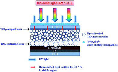
We have tested the bare and phosphor coated photoanodes (dye-sensitized TiO2 films) under different conditions to study their photostability. This has been done in order to identify the degradation mechanism occurring in the most important component of a DSSC (photoanode). This is in contrast to majority of other previous studies, which deal with the degradation mechanism of the complete device in which the electrolyte bleaching, sealing failures, moisture ingress and thermal stress have been found to be the main reasons for device degradation.12–18 In the present work, we have tested bare and phosphor coated photoanodes, and also complete DSSCs, to shed more light on the degradation processes in a DSSC. We also demonstrate the improved light stability of DS NPs coated photoanodes and DSSCs. Fig. 1 shows a schematic of a DSSC coated with DS nanophosphor on top side, i.e. reverse of photoanode.
2. Experimental details
2.1 Synthesis of YVO4:Eu3+ down-shifting nanophosphor
The nanophosphor was prepared by a chemical co-precipitation (CCP) method reported previously.19 Stoichiometric quantities of precursors yttrium oxide (Y2O3), vanadium pentoxide (V2O5), europium oxide (Eu2O3) were taken according to the chemical formula Y1−xVO4:Eux. On varying europium concentration (x = 0.05–0.13), x = 0.11 was found to be the most suitable concentration for having maximum PL intensity. Oxide precursors were dissolved in minimum amount of HCl separately. The precursor solutions were mixed by ultrasonication and HNO3![[thin space (1/6-em)]](https://www.rsc.org/images/entities/char_2009.gif) :
:![[thin space (1/6-em)]](https://www.rsc.org/images/entities/char_2009.gif) H2O2 in volume ratio 3
H2O2 in volume ratio 3![[thin space (1/6-em)]](https://www.rsc.org/images/entities/char_2009.gif) :
:![[thin space (1/6-em)]](https://www.rsc.org/images/entities/char_2009.gif) 1 was added to the above mixture in order to convert the precursors to soluble nitrates. NH4OH and H2O2 in the volume ratio 3
1 was added to the above mixture in order to convert the precursors to soluble nitrates. NH4OH and H2O2 in the volume ratio 3![[thin space (1/6-em)]](https://www.rsc.org/images/entities/char_2009.gif) :
:![[thin space (1/6-em)]](https://www.rsc.org/images/entities/char_2009.gif) 1 was added drop wise into the solution till the pH of the solution was ∼8, when ultrafine particles of YVO4:Eu started forming. Thus precipitated nanoparticles were separated out using a centrifuge. YVO4:Eu nanoparticles were washed three times with methanol to dehydrate the surface bound water molecules. The NPs were then stabilized in 5% solution of SHMP in chloroform with rigorous ultrasonication. Finally, the collected precipitates were dried in a vacuum oven at 40 °C for 12 h. Starting with ∼4 grams of precursors, about 1.5 gram NPs were finally obtained, providing a yield of ∼38% for the CCP method.
1 was added drop wise into the solution till the pH of the solution was ∼8, when ultrafine particles of YVO4:Eu started forming. Thus precipitated nanoparticles were separated out using a centrifuge. YVO4:Eu nanoparticles were washed three times with methanol to dehydrate the surface bound water molecules. The NPs were then stabilized in 5% solution of SHMP in chloroform with rigorous ultrasonication. Finally, the collected precipitates were dried in a vacuum oven at 40 °C for 12 h. Starting with ∼4 grams of precursors, about 1.5 gram NPs were finally obtained, providing a yield of ∼38% for the CCP method.
2.2 DSSC fabrication and coating of YVO4:Eu3+ nanoparticles on solar cells
A mesoporous TiO2 layer of thickness ∼12 μm and a scattering layer of ∼4 μm were deposited by doctor blade method using commercially available pastes (Dyesol 18NR-T and WER2-O). Subsequently, the film was immersed in 40 mM aqueous TiCl4 solution at 70 °C for 30 min, then rinsed with DI water and annealed at 500 °C in air for 15 min. For fabricating DS-DSSCs, down-shifting NPs were spray coated on reverse of FTO, i.e. on the non-conducting side, by spraying a ∼1.5 mg ml−1 dispersion of DS NPs in propanol at 175 °C (see Fig. 1). This deposition was performed after the annealing of TiCl4 treated films. For fabricating control DSSCs, the DS NPs coating step was not performed. The TiO2 films were immersed in 0.3 mM ethanol solution of N719 dye for ∼18 h. Thin films of platinum (∼100 nm) were sputter coated on FTO and used as counter electrodes. The DSSCs were assembled in a sandwich configuration with dye sensitized TiO2 anode and platinum cathode. The electrolyte consisting of 0.1 M LiI, 0.05 M I2, 0.5 M tert-butylpyridine (TBP) and 0.6 M 1-propyl-2,3-dimethyl imidazolium iodide (DMPII) in acetonitrile was injected between the two electrodes. The two electrodes were held using binder clips. For preparing sealed DSSCs, Surlyn (DuPont) was used as a sealant to hold together the TiO2 photoanode and Pt counter electrode. Thus prepared DSSCs, with a geometrical area of 1 cm × 1 cm, were tested with an aperture of 8 mm × 8 mm to define an active area of ∼0.64 cm2.2.3 Instruments
Photovoltaic performances of control DSSC and DS-DSSC devices were evaluated using I–V measurement system (Class AAA solar simulator, Sol3A, Oriel Newport, USA with Keithley 2440 sourcemeter) and incident photon to current conversion efficiency (IPCE) measurement system (ReRa Solutions, The Netherlands). Electrochemical impedance spectroscopy studies were also performed, under AM1.5G illumination, for some of the DSSCs using Zahner Zennium (Germany) electrochemical workstation. X-ray diffraction (XRD) pattern of phosphor sample was obtained by Rigaku Ultima IV XRD system in a 2θ range of 20°–50° using Cu-Kα radiation (λ = 1.54 Å). Energy dispersive X-ray spectrum (EDS) of the YVO4:Eu3+ nanophosphor was recorded using Hitachi TM3000 table-top scanning electron microscope (SEM) equipped with SwiftED 3000 EDX detector. Tecnai G2 S-TWIN transmission electron microscope (TEM) was used to record TEM image of nanoparticles at an acceleration voltage of 200 kV. Photoluminescence (PL) emission and excitation spectra of DS nanophosphor were recorded using a combined steady state fluorescence and phosphorescence lifetime spectrometer (Edinburgh instrument model FLS920).2.4 Stability testing of control DSSC and DS-DSSC photoanodes
The photoanodes of control DSSCs and DS DSSCs were tested under three different illumination conditions. (1) One DSSC photoanode of each type was tested under continuous illumination provided by a solar simulator (Sol3A, Oriel) for 24 h. (2) One photoanode of each type (bare and phosphor coated) was tested under a laboratory UVA (λ ∼ 365 nm) lamp (Haichao F6T5/BLB, 6 W, Blacklight blue) for 500 h. The DSSC photoanodes and the lamp were kept at a distance of 20 cm in an enclosed box. The lamp was switched on for ∼10 h duration each day and the process was continued for about 50 days. The anodes were stored in a dessicator under dark conditions while the lamp was off. (3) One photoanode of each type was kept in a sealed glass Petri-dish outside in the open on a south facing inclined surface (see Fig. 2). This experiment was performed in April 2014. April is the month when the incident solar radiation is very high in New Delhi (∼900 W m−2).20 The photoanodes were kept in the open continuously for a duration of 26 days and photovoltaic parameters were recorded three times in between. It was observed that direct sunlight was incident on the samples for almost 7 h each day and maximum temperature reached ∼35–40 °C in afternoons. The highest temperature of 43 °C was recorded on 30 April 2014, which was the 26th and last day of the experiment. Apart from the photoanodes, one complete sealed DSSC of each type (bare and nanophosphor coated) was tested under illumination of a solar simulator for 24 h.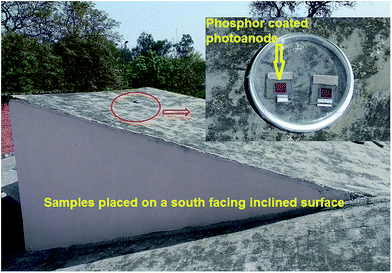 | ||
| Fig. 2 Bare and phosphor coated photoanodes kept in a sealed glass Petri-dish outside in the open on a south facing inclined surface. | ||
The photoanodes under illumination for stability testing were removed from the experimental setup periodically to record I–V parameters. For the photoanode kept outside in the open, IPCE was also recorded. To perform these measurements, the photoanodes were assembled in a sandwich configuration with Pt counter electrode and electrolyte was injected between them. Since the Pt electrode and electrolyte were not subjected to light exposure, any degradation in DSSC performance was ascribed to degradation of photoanode components. The detailed discussion is presented later in the manuscript.
3. Results and discussion
3.1 YVO4:Eu3+ down-shifting nano-phosphor
Fig. 3a shows the XRD pattern of the synthesized phosphor NPs. The recorded XRD pattern of the synthesized YVO4 NPs matches well with the standard diffraction pattern (JCPDS Card No. 17-0341) of the zirconia type tetragonal structure of YVO4 with three prominent peaks corresponding to (h k l) indices (2 0 0), (1 1 2) and (3 1 2). Other peaks are also labeled with appropriate indices according to the standard diffraction pattern. There is one unassigned peak near 28°, which might be due to the presence of other crystal phase of yttrium vanadate in the sample. The EDS analysis of the nanophosphor revealed the presence of europium in addition to yttrium, vanadium and oxygen; this indicates that europium was successfully doped in the crystalline yttrium vanadate host (see Fig. S1, ESI†). The TEM image of the phosphor NPs is shown in Fig. 3b. The NPs are less than 5 nm in size. Some NPs have been circled and marked with arrows in the TEM image for identification. The inverted color TEM image is also shown in the ESI (Fig. S2, ESI†). It can be clearly seen that the particle size is less than 5 nm. The nanophosphor exhibits a broad absorption spectrum in the 300–350 nm range, with a peak centered at 320 nm (see Fig. 4, blue dotted curve). The emission from nanophosphor lies in the red region and shows a sharp peak centered at 618 nm (Fig. 4, red dash-dotted curve). Absoprtion spectrum of N719 dye, used as a sensitizer in the present work, is also shown for comparison (Fig. 4, green dashed curve). The dye does not absorb in 300–360 nm region, while the nanophosphor absorbs in the 300–350 nm region. Thus, the nanophosphor complements the dye absorption in UV region. The red emission from nanophosphor can be absorbed by the dye molecules. AM1.5 spectra is shown for reference; the emission and absorption spectra of nanophosphor match well with the AM1.5 spectra, indicating that down-shifting is a promising approach for harvesting the UV portion of the solar spectrum received on earth's surface.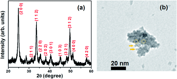 | ||
| Fig. 3 (a) X-ray diffraction pattern, (b) TEM image of YVO4:Eu3+ phosphor nanoparticles synthesized by a chemical co-precipitation method. | ||
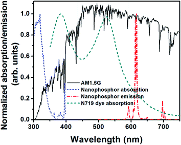 | ||
| Fig. 4 Photoluminescence excitation and emission spectra of YVO4:Eu3+ down shifting phosphor nanoparticles. Absorption spectrum of N719 dye and the standard AM1.5 spectrum are also shown. | ||
3.2 Effects of down-shifting nanophosphor on DSSC performance
To optimize the spray volume, i.e. the quantity, of phosphor dispersion in order to obtain an optimum performance from the device, three different (5, 10, 15 ml) spray volumes (of 1.5 mg ml−1 NP dispersion) were coated on reverse of FTO substrates. Coating with spray volumes of 10 and 15 ml resulted in a significant reduction in transmittance of FTO substrates (see Fig. S4, ESI†). Therefore, only 5 ml dispersion has been spray coated on reverse of FTO to fabricate DS-DSSCs. This spray volume provides a balance between good transmittance and sufficient down-shifting effect required to protect the device from UV photons. A trade-off between these two factors is necessary to obtain photocurrent enhancement and improve stability at the same time.
| Device (Device-ID) | Open circuit voltage, VOC (mV) | Short-circuit current density, JSC (mA cm−2) | Fill factor, FF (%) | Efficiency, η (%) | Increase in photo-current |
|---|---|---|---|---|---|
| Control DSSC (A1) | 765 | 15.9 | 65.2 | 7.93 | — |
| DS-DSSC (A2) | 770 | 16.5 | 65.5 | 8.32 | 3.8% (0.6 mA cm−2) |
| Control DSSC (B1) | 767 | 16.1 | 63.9 | 7.89 | — |
| DS-DSSC (B2) | 771 | 16.6 | 64.3 | 8.23 | 3.1% (0.5 mA cm−2) |
| Control DSSC (C1) | 749 | 15.1 | 71 | 8 | — |
| DS-DSSC (C2) | 760 | 15.5 | 71 | 8.36 | 2.65% (0.4 mA cm−2) |
| Control DSSC (D1) sealed | 712 | 16.3 | 65.5 | 7.6 | — |
| DS-DSSC (D2) sealed | 715 | 16.8 | 66 | 7.92 | 3.1% (0.5 mA cm−2) |
An average enhancement of 0.5 ± 0.1 mA cm−2 is obtained by using the phosphor NPs on top of DSSCs. The open circuit voltages and fill factors of DS-DSSCs are almost same as that of control DSSCs. This indicates that the coupling between the phosphor NPs and the solar cell is purely optical in nature. There is no decrease in open circuit voltages and fill factor because the NPs are not in direct contact with the active layer of the solar cell. These results suggest that the optimized thin layer of DS NPs should be placed on top of a solar cell without reducing the transmission of incident light, and not be in physical contact with the dye-sensitized TiO2 active layer.
The UV spectral response of DSSCs is relatively low because of large refractive index mismatch between air and FTO substrate which leads to a high reflectance loss in the UV-blue region. The DS nanophosphor can overcome this limitation as it down-shifts high energy photons to low energy red photons, which can then be absorbed by the dye molecules. The IPCE spectra of devices A1 and A2 are shown in Fig. 5. There is a small enhancement of photocurrent in the short-wavelength region of 350–450 nm. This is because of the absorption of UV photons and subsequent re-emission of visible photons by the phosphor layer coated on top of DSSC. A small enhancement in 600–700 nm range is also observed, which can be attributed to scattering effects of the phosphor layer, which is somewhat rough in nature and also consists of large (∼200 nm) particle clusters (see Fig. S5, ESI†).21 Such enhancements in IPCE have also been observed for Si and perovskite solar cells utilizing a down-shifting nanophosphor layer.21–23 It is somewhat counter-intuitive to observe an enhancement in short-wavelength IPCE by use of nanophosphor. But, it must be understood that, since the increase in photocurrent is in response to UV-blue light, an increase in UV-blue spectral response must be expected; which is indeed observed experimentally. Although, the enhancement obtained by use of DS NPs is small, it is an additional benefit considering the fact that long-term stability under illumination is improved.
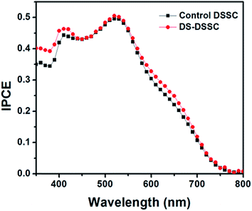 | ||
| Fig. 5 IPCE spectra of control DSSC (device A1) and DS-DSSC (device A2) showing enhancement in short wavelength region. | ||
In general, the DS-DSSCs are more stable than control DSSCs under different illumination conditions. Table 2 shows the photovoltaic parameters of DSSCs after illumination under different conditions for varying time periods. We discuss the stability of phosphor coated devices in detail in the following sections.
| Device (Device-ID) | Open circuit voltage, VOC (mV) | Short-circuit current density, JSC (mA cm−2) | Fill factor, FF (%) | Efficiency, η (%) |
|---|---|---|---|---|
| After 24 hours under a solar simulator | ||||
| Control DSSC (A1) | 755 | 11.7 | 56 | 4.95 |
| DS-DSSC (A2) | 766 | 14.9 | 64 | 7.30 |
| Control DSSC (D1) (sealed cell) | 710 | 13.1 | 65 | 6.05 |
| DS-DSSC (D2) (sealed cell) | 712 | 15.8 | 66 | 7.42 |
![[thin space (1/6-em)]](https://www.rsc.org/images/entities/char_2009.gif) |
||||
| After 500 hours of illumination under a UV lamp | ||||
| Control DSSC (B1) | 701 | 10.2 | 61 | 4.36 |
| DS-DSSC (B2) | 745 | 13.3 | 62 | 6.15 |
![[thin space (1/6-em)]](https://www.rsc.org/images/entities/char_2009.gif) |
||||
| After 26 days in outdoor conditions | ||||
| Control DSSC (C1) | 590 | 5.6 | 63 | 2.08 |
| DS-DSSC (C2) | 671 | 10.3 | 62 | 4.29 |
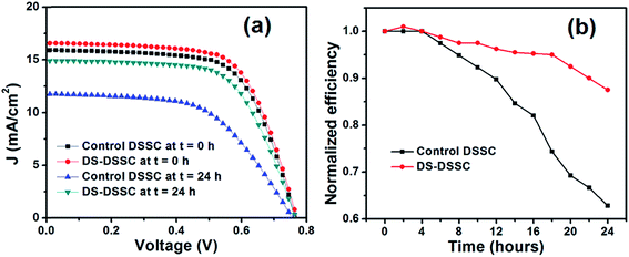 | ||
| Fig. 6 (a) Current density–voltage graphs and (b) time variations in efficiencies of devices A1 (control DSSC) and A2 (DS-DSSC). | ||
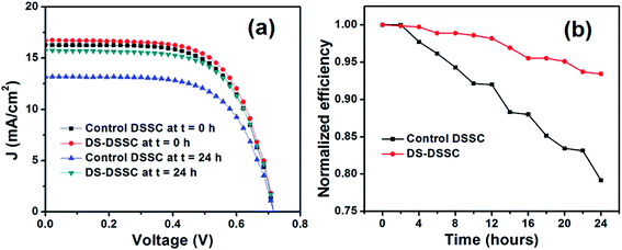 | ||
| Fig. 7 (a) Current density–voltage graphs and (b) time variations in efficiencies of devices D1 (control DSSC) and D2 (DS-DSSC). | ||
The efficiencies of the unsealed devices A1 and A2 degrade gradually with illumination time (see Fig. 6b). After 24 h, the DS-DSSC degrades to ∼87% of its initial efficiency. On the other hand, the control DSSC degrades to ∼62% of its initial efficiency. This result clearly points out to the protection offered by DS NPs to the DSSC photoanode. It must be mentioned here that open circuit voltage and fill factor show negligible change after 24 h, and the photocurrent decrement is the main factor responsible for overall degradation in the device efficiency. Since, only the photoanodes have been kept under illumination, the factors related to electrolyte and counter electrode degradation can be discounted as possible mechanisms for efficiency decrement. Instead, dye molecule structural changes by high energy UV-blue photons and electron trapping by UV-induced trap states in TiO2 (oxygen vacancies) are the primary degradation mechanisms.12,24,25
The variations in efficiencies of sealed DSSCs are shown in Fig. 7b. It can be observed that sealed devices perform better than the unsealed photoanodes. This is because the acetonitrile in the electrolyte solution is able to partially fill the TiO2 surface trap states.26,27 Also, the excited dye molecules are quickly regenerated by the electrolyte and chances of any changes in the molecular structure are avoided. However, in a complete sealed cell, another degradation mechanism, electrolyte bleaching (depletion of electrolyte), comes into play.13–15 The degradation of electrolyte is accelerated under UV illumination.14 We observe that the efficiency of control DSSC falls to ∼80% of its initial efficiency after 24 h of illumination. The DS-DSSC fares much better and retains almost 95% of its initial efficiency (see Fig. 7b). This observation implies that light (especially UV) degradation effects in the DSSCs are mainly responsible for decrease in efficiency, and DS NPs are able to prevent this UV degradation to a great extent. Here also, the VOC and FF are not affected significantly and the efficiency degradation is primarily because of photocurrent decrement.
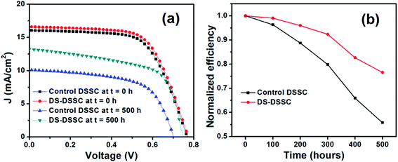 | ||
| Fig. 8 (a) Current density–voltage graphs and (b) time variations in efficiencies of devices B1 (control DSSC) and B2 (DS-DSSC) under the illumination of a UV lamp. | ||
For the first 100 h of UV illumination, the efficiencies of the devices are not degraded much and remain above 95% of the initial values (see Fig. 8b). After 100 h, the efficiencies begin to decrease. Control DSSC is degraded to ∼55% of its initial efficiency, while DS-DSSC retains almost 77% of its efficiency after 500 h of UV illumination. Since the power of UV lamp used is rather low, the relatively stable performance obtained for the first 100 h can be explained on the basis of stability of the device components (TiO2 and dye molecules) during this period. After a prolonged UV exposure, TiO2 becomes increasingly hydrophilic and attracts environmental moisture on its surface.25,28 The presence of water along with UV radiation results in a loss of thiocyanate (SCN−) ligands from the dye molecules. This happens due to ligand exchange between SCN− and H2O/OH− and also due to loss of SCN− ligand in air.12 The dye molecules get degraded in this manner and as a consequence, the photocurrent and efficiency of the device go down.
DS-DSSC shows relatively less decrease in photocurrent and efficiency, and retains almost 75% of its initial efficiency while control DSSC degrades to ∼55% of initial efficiency. It implies that the UV degradation effects are mitigated by DS phosphor NPs. A small decrease of 20–30 mV is also observed in VOC of both the cells. This may be because of reduced ISC, which results in a lower VOC because of the voltage dependence on ISC according to the relation,
 | (1) |
The bare and phosphor coated photoanodes (devices C1 and C2) were kept outside on a south facing inclined surface to maximize the time and amount of solar radiation incident on the sample (see Fig. 2). Fig. 9 shows pictures of the photoanodes at t = 0 and t = 26 days. The bare photoanode shows discoloration after 26 days while the phosphor coated anode seems to be unaffected. The J–V curves and time variations in efficiencies of the two devices are shown in Fig. 10a and b, respectively.
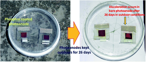 | ||
| Fig. 9 Photographs of bare and phosphor coated photoanodes taken at the start (t = 0 days) and end (t = 26 days) of the experiment. | ||
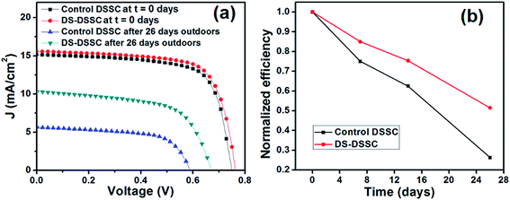 | ||
| Fig. 10 (a) Current density–voltage graphs and (b) time variations in efficiencies of devices C1 (control DSSC) and C2 (DS-DSSC) kept in outdoor conditions. | ||
The DS-DSSC performs much better than control device and retains more than 60% of its efficiency, while the control DSSC falls to less than 30% of its initial efficiency. It can be seen from Fig. 10a that all the photovoltaic parameters (JSC, VOC and FF) of DSSCs are degraded after 26 days (see Table 2). The discoloration of the bare photoanode suggests that the molecular structure of the dye is disturbed and the modified structure is unable to absorb the incident light effectively. This can happen due to the loss of SCN− ligands from the dye molecules. The ligand loss is accelerated under illumination and humid conditions, and a blue-shift in absorption maxima of the dye occurs.12 It has been suggested earlier that UV radiation and moisture need to be excluded in order to obtain a long and stable life of dye molecules.12
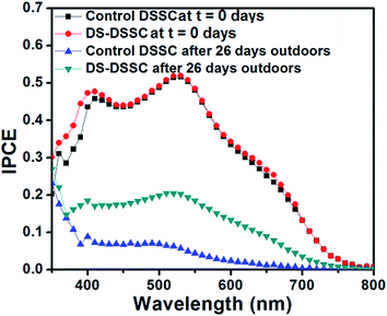
Fig. 11 shows the IPCE spectra of fresh and degraded DSSCs. The control DSSC's IPCE spectrum shows a flattening and blue-shift of the peak maximum from 530 to 500 nm. The IPCE peak maximum of DS-DSSC shifts from 530 to 520 nm, although the IPCE spectrum retains most of its original features. This is consistent with the results obtained by Agrell et al., where this observation has been explained on the basis of loss of SCN− ligand.12 The thiocyanate ion ligand is also exchanged with H2O/OH− and this process is much faster under illumination of visible and UV radiation. The improved performance obtained for DS NPs coated DSSC is because of the down-shifting of UV photons to visible region. Despite the phosphor coating, DS-DSSC also shows a loss of ∼48% in efficiency because the visible light is also partially responsible for device degradation. Apart from illumination, the thermal stress experienced by the device in outdoor conditions may also result in some degradation of dye molecules.12–18
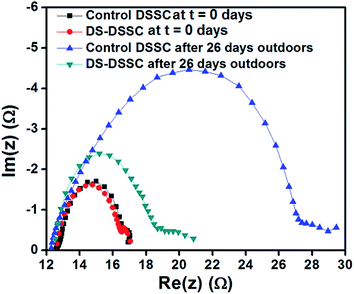
To obtain further insights into the degradation observed in DSSC photoanodes, fresh and degraded cells were analyzed using electrochemical impedance spectroscopy (EIS) under AM1.5G illumination. Fig. 12 shows the Nyquist plots of bare and phosphor coated DSSCs recorded immediately after fabrication and after 26 days of outdoor testing. The main central arc occurs in the mid-frequency region, which corresponds to the TiO2–dye–electrolyte interface.31–33 The effective electron lifetimes can be calculated using the relation, τeff = 1/(2πfm), where fm is the frequency corresponding to the peak phase in the mid-frequency region of the Bode phase plot as shown in Fig. 13.32
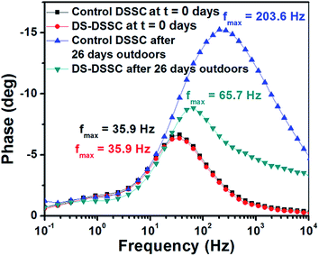 | ||
| Fig. 13 Bode plots of control and DS-DSSCs showing the frequencies corresponding to the phase peak in mid-frequency regions. | ||
In Fig. 12, the diameter of the central arc corresponds to the charge transfer resistance (RTiO2) at the TiO2–dye–electrolyte interface. Both the fresh cells have a RTiO2 of about 4 ohms. After degradation, the RTiO2 of control DSSC increases to ∼14 ohms, while that of DS-DSSC increases to ∼6 ohms. The calculated effective electron lifetimes in control DSSC decrease from 4.43 ms to 0.78 ms; and in DS-DSSC decrease from 4.43 ms to 2.42 ms (see Fig. 13). The increased resistance to charge transfer arises due to trap states in TiO2 originating from UV and thermal stresses.13,14,30 Due to ligand loss, the effective number of absorbing dye molecules, and hence the photoelectrons decrease and also the remaining electrons can be captured by the trap states of TiO2. Thus, recombination increases leading to a decrease in effective electron lifetimes.
The DS-DSSC is subjected to same visible illumination and thermal stresses as those suffered by control DSSC. Still, the effective electron lifetimes for DS-DSSC are greater and RTiO2 is lesser than control DSSC. Also, control DSSC shows a prominent discoloration due to dye degradation (see Fig. 9), while DS-DSSC does not. These observations indicate that UV radiation is the major factor responsible for degradation of dye molecules by ligand loss/exchange and creation of trap states in TiO2. The use of YVO4:Eu3+ DS phosphor NPs mitigates the UV induced degradations and consequently, the DS-DSSC performs much better than the control DSSC under actual outdoor working conditions. This approach can facilitate the fabrication of highly efficient and stable DSSCs in a versatile and facile manner. Our simple spray deposition technique can be easily adopted for other solar cell technologies. We have already shown the improved performance of perovskite solar cells, by utilizing the general approach mentioned above, in a previous work.23 Our study clearly demonstrates the beneficial effects of using the DS material for improving the stability of DSSCs. The optimized value of spray volume represents a balance between: (1) good transmittance, (2) photocurrent enhancement, and (3) UV protection in the DSSC.
4. Conclusions
The work presented in this paper clearly demonstrates the dual benefits of using YVO4:Eu3+ down-shifting phosphor nanoparticles: enhancement in photocurrent and improved stability under illumination of DSSCs. Through detailed experiments, it has been deduced that UV light is a major factor in degradation of DSSC performance. The phosphor NPs can be spray coated on top of DSSCs to provide UV protection and also improve the short-wavelength spectral response of the devices. A down-shifting material with a broad absorption band, which effectively absorbs the 300–400 nm portion of the UV spectrum, would be an ideal choice for improving photocurrent and UV stability of solar cells. Our results may open up further avenues for improving the performance of DSSCs.Acknowledgements
N. C. and V. K. K. acknowledge the funding from Department of Science & Technology (DST), Govt. of India, grant number RP02914 under Solar Energy Enabling Research. The authors also thank Mr Akshay Kaushal for TEM characterization.References
- S. Mathew, A. Yella, P. Gao, R. Humphry-Baker, B. F. E. Curchod, N. Ashari-Astani, I. Tavernelli, U. Rothlisberger, M. K. Nazeeruddin and M. Grätzel, Nat. Chem., 2014, 6, 242–247 CrossRef CAS PubMed
.
- M. Durr, A. Bamedi, A. Yasuda and G. Nelles, Appl. Phys. Lett., 2004, 84, 3397 CrossRef CAS PubMed
.
- M. Yanagida, N. Onozawa-Komatsuzaki, M. Kurashige, K. Sayama and H. Sugihara, Sol. Energy Mater. Sol. Cells, 2010, 94, 297–302 CrossRef CAS PubMed
.
- N. Chander, A. F. Khan, E. Thouti, S. K. Sardana, P. S. Chandrasekhar, V. Dutta and V. K. Komarala, Sol. Energy, 2014, 109, 11–23 CrossRef CAS PubMed
.
- N. Chander, P. Singh, A. F. Khan, V. Dutta and V. K. Komarala, Thin Solid Films, 2014, 568, 74–80 CrossRef CAS PubMed
.
- G. B. Shan and G. P. Demopoulos, Adv. Mater., 2010, 22, 4373–4377 CrossRef CAS PubMed
.
- J. Liu, Q. Yao and Y. Li, Appl. Phys. Lett., 2006, 88, 173119 CrossRef PubMed
.
- Z. Hosseini, W. K. Huang, C. M. Tsai, T. M. Chen, N. Taghavinia and E. W. G. Diau, ACS Appl. Mater. Interfaces, 2013, 5, 5397–5402 CAS
.
- Y. J. Lin, C. C. Chang, S. J. Cherng, J. W. Chen and C. M. Chen, Prog. Photovoltaics, 2015, 23, 106–111 CAS
.
- A. F. Khan, R. Yadav, P. K. Mukhopadhya, S. Singh, C. Dwivedi, V. Dutta and S. Chawla, J. Nanopart. Res., 2011, 13, 6837–6846 CrossRef CAS
.
- F. Bella, G. Griffini, M. Gerosa, S. Turri and R. Bongiovanni, J. Power Sources, 2015, 283, 195–203 CrossRef CAS PubMed
.
- H. G. Agrell, J. Lindgren and A. Hagfeldt, Sol. Energy, 2003, 75, 169–180 CrossRef
.
- D. Bari, N. Wrachien, G. Meneghesso, C. Andrea, R. Tagliaferro, T. M. Brown, A. Reale and A. Di Carlo, IEEE International Reliability Physics Symposium (IRPS), 2013, 4B.3.1, DOI:10.1109/irps.2013.6532011
.
- K. F. Jensen, W. Veurman, H. Brandt, C. Im, J. Wilde and A. Hinsch, MRS Online Proc. Libr., 2013, 1537, DOI:10.1557/opl.2013.790
, mrss13-1537-b11-14.
- N. Kato, Y. Takeda, K. Higuchi, A. Takeichi, E. Sudo, H. Tanakaa, T. Motohiro, T. Sano and T. Toyoda, Sol. Energy Mater. Sol. Cells, 2009, 93, 893–897 CrossRef CAS PubMed
.
- M. Berginc, U. O. Krašovec and M. Topič, Sol. Energy Mater. Sol. Cells, 2014, 120, 491–499 CrossRef CAS PubMed
.
- S. Mastroianni, A. Lanuti, S. Penna, A. Reale, T. M. Brown, A. D. Carlo and F. Decker, ChemPhysChem, 2012, 13, 2925–2936 CrossRef CAS PubMed
.
- S. Mastroianni, I. Asghar, K. Miettunen, J. Halme, A. Lanuti, T. M. Brown and P. Lund, Phys. Chem. Chem. Phys., 2014, 16, 6092–6100 RSC
.
- A. F. Khan, D. Haranath, R. Yadav, S. Singh, S. Chawla and V. Dutta, Appl. Phys. Lett., 2008, 93, 073103 CrossRef PubMed
.
- Solar radiant energy over India, ed. A. P. Tyagi, Indian Meteorological Department, Ministry of Earth Sciences, Govt. of India, 2009 Search PubMed
.
- C. K. Huang, Y. C. Chen, W. B. Hung, T. M. Chen, K. W. Sun and W. L. Chang, Prog. Photovoltaics, 2013, 21, 1507–1513 CAS
.
- N. Chander, S. K. Sardana, P. K. Parashar, A. F. Khan, S. Chawla and V. K. Komarala, IEEE J. Photovolt., 2015 DOI:10.1109/jphotov.2015.2438633
.
- N. Chander, A. F. Khan, P. S. Chandrasekhar, E. Thouti, S. K. Swami, V. Dutta and V. K. Komarala, Appl. Phys. Lett., 2014, 105, 033904 CrossRef PubMed
.
- T. Leijtens, G. E. Eperon, S. Pathak, A. Abate, M. M. Lee and H. J. Snaith, Nat. Commun., 2013, 4, 2885 Search PubMed
.
- T. Zubkov, D. Stahl, T. L. Thompson, D. Panayotov, O. Diwald and J. T. Yates, Jr, J. Phys. Chem. B, 2005, 109, 15454–15462 CrossRef CAS PubMed
.
- R. da Silva, L. G. C. Rego, J. A. Freire, J. Rodriguez, D. Laria and V. S. Batista, J. Phys. Chem. C, 2010, 114, 19433–19442 CAS
.
- J. Nelson, A. M. Eppler and I. M. Ballard, J. Photochem. Photobiol., A, 2002, 148, 25–31 CrossRef CAS
.
- J. Schneider, M. Matsuoka, M. Takeuchi, J. Zhang, Y. Horiuchi, M. Anpo and D. W. Bahnemann, Chem. Rev., 2014, 114, 9919–9986 CrossRef CAS PubMed
.
- M. K. Nazeeruddin, R. Humphry-Baker, P. Liska and M. Grӓtzel, J. Phys. Chem. B, 2003, 107, 8981–8987 CrossRef CAS
.
- E. Figgemeier and A. Hagfeldt, Int. J. Photoenergy, 2004, 6, 127–140 CrossRef CAS
.
- Dye-sensitized solar cells, ed. K. Kalyansundaram, EPFL Press, Lausanne (Switzerland), 2010, ch. 12 Search PubMed
.
- R. Kern, R. Sastrawan, J. Ferber, R. Stangl and J. Luther, Electrochim. Acta, 2002, 47, 4213–4225 CrossRef CAS
.
- N. Chander, P. S. Chandrasekhar and V. K. Komarala, RSC Adv., 2014, 4, 55658–55665 RSC
.
Footnote |
| † Electronic supplementary information (ESI) available. See DOI: 10.1039/c5ra10067d |
| This journal is © The Royal Society of Chemistry 2015 |

