
A graphene–Mo2C heterostructure for a highly responsive broadband photodetector†
Xiaozhi
Bao
a,
Tian
Sun
b,
Yan
Liu
b,
Chuan
Xu
c,
Weiliang
Ma
b,
Junpo
Guo
a,
Yun
Zheng
a,
Shivananju Bannur
Nanjunda
d,
Huating
Liu
e,
Zongyu
Huang
 e,
Shaojuan
Li
bf,
Shenghuang
Lin
g,
Guichuan
Xing
a,
Wencai
Ren
*c,
Qiaoliang
Bao
*b and
Huaiyu
Shao
*a
e,
Shaojuan
Li
bf,
Shenghuang
Lin
g,
Guichuan
Xing
a,
Wencai
Ren
*c,
Qiaoliang
Bao
*b and
Huaiyu
Shao
*a
aGuangdong-Hong Kong-Macau Joint Laboratory for Photonic-Thermal-Electrical Energy Materials and Devices, Institute of Applied Physics and Materials Engineering, University of Macau, Avenida da Universidade, Taipa, Macao SAR 999078, China. E-mail: hshao@um.edu.mo
bInstitute of Functional Nano and Soft Materials (FUNSOM), Soochow University, Suzhou 215123, P. R. China. E-mail: qiaoliang.bao@gmail.com
cShenyang National Laboratory for Materials Science, Institute of Metal Research, Chinese Academy of Sciences, Shenyang 110016, P. R. China. E-mail: wcren@imr.ac.cn
dDepartment of Electrical Engineering, Centre of Excellence in Biochemical Sensing and Imaging Technologies (Cen-Bio-SIM), Indian Institute of Technology Madras, Chennai 600036, India
eHunan Key Laboratory for Micro-Nano Energy Materials and Devices, School of Physics and Optoelectronic, Xiangtan University, Hunan 411105, China
fState Key Laboratory of Applied Optics, Changchun Institute of Optics, Fine Mechanics and Physics, Chinese Academy of Sciences, Changchun, Jilin, 130033, China
gSongshan Lake Materials Laboratory, Dongguan 523808, China
First published on 15th September 2021
Abstract
Photodetectors based on intrinsic graphene can operate over a broad wavelength range with ultrafast response, but their responsivity is much lower than commercial silicon photodiodes. The combination of graphene with two-dimensional (2D) semiconductors may enhance the light absorption, but there is still a cutoff wavelength originating from the bandgap of semiconductors. Here, we report a highly responsive broadband photodetector based on the heterostructure of graphene and transition metal carbides (TMCs, more specifically Mo2C). The graphene–Mo2C heterostructure enhanced light absorption over a broad wavelength range from ultraviolet to infrared. In addition, there is very small resistance for photoexcited carriers in both graphene and Mo2C. Consequently, photodetectors based on the graphene–Mo2C heterostructure deliver a very high responsivity from visible to infrared telecommunication wavelengths.
Owing to its unique band structure with the zero bandgap and linear dispersion near Dirac point, graphene holds great potential for many broadband photonic and optoelectronic device applications such as broadband polarizers,1 broadband modulators,2 transparent electrodes3 and broadband photodetectors.4–6 One atomic layer graphene can absorb ∼2.3% of incident light7 over a broadband wavelength from ultraviolet to terahertz. In addition, graphene also shows high carrier mobility (up to 200
![[thin space (1/6-em)]](https://www.rsc.org/images/entities/char_2009.gif) 000 cm2 V−1 S−1)8,9 and fast photoelectric response (up to 40 GHz),6 which makes graphene a promising candidate for ultrafast and ultra-broadband photodetection. Nevertheless, the photo-responsivity of an intrinsic graphene photodetector is at the scale of 10 mA W−15, which is three orders of magnitude lower than the commercially available silicon-based photodiodes in the visible range, because of the relatively low absolute absorptance and huge recombination of photo-generated carriers. Many efforts have been made to improve the responsivity of the graphene-based photodetector, including the integration of graphene with plasmonic structures10,11 or microcavities,12 but the fabrication process is complex, and the responsivity is still as low as several tens of mA W−1.
000 cm2 V−1 S−1)8,9 and fast photoelectric response (up to 40 GHz),6 which makes graphene a promising candidate for ultrafast and ultra-broadband photodetection. Nevertheless, the photo-responsivity of an intrinsic graphene photodetector is at the scale of 10 mA W−15, which is three orders of magnitude lower than the commercially available silicon-based photodiodes in the visible range, because of the relatively low absolute absorptance and huge recombination of photo-generated carriers. Many efforts have been made to improve the responsivity of the graphene-based photodetector, including the integration of graphene with plasmonic structures10,11 or microcavities,12 but the fabrication process is complex, and the responsivity is still as low as several tens of mA W−1.
Other two-dimensional (2D) materials, such as transition metal dichalcogenides (TMDs), are gaining increasing attention as promising channel materials for field-effect transistors (FETs). Monolayer TMDs are direct-bandgap semiconductors,13 which are suitable for applications in optoelectronic devices because of the high absorption coefficient and efficient electron–hole pair generation under photoexcitation.14 Constructing van der Waals heterostructures consisting of graphene and TMD is an effective approach to combine the merits of both materials. In particular, graphene–MoS215 or graphene–WSe216 heterostructure photodetectors have shown unprecedented performance in terms of high responsivity and sensitivity because of the efficient generation of photocarriers by TMDs and high carrier mobility of graphene. However, the large bandgap (1–2.5 eV17,18) and relatively low mobility (10–250 cm2 V−1 s−1) in TMDs impede broadband photodetection, particularly in telecommunication bands around 1550 nm.
Recently, 2D transition metal carbides (TMCs) have been synthesized, which have shown amazing optical and electronic properties.19,20 As a result, from the incorporation of carbon atoms into the metal lattice, transition metal carbides are a large family of materials, which combine the properties of ceramics and metals.21 Particularly, they have superior mechanical properties, high stability and melting points, good thermal shock resistance and low chemical reactivity. Many TMCs, such as Mo2C, W2C, WC, NbC and TaC also show superconductivity and excellent catalytic activity.21–23 As one of the mostly studied TMCs, Mo2C has high electron density at the Fermi level, affording high electronic conductivity and good nonlinear optical properties.24,25 Mo2C has two stable crystalline forms, orthorhombic α-Mo2C and hexagonal β-Mo2C, in which carbon atoms show distinct ordered and disordered distributions, respectively. It is nontrivial to prepare Mo2C nanosheets with desired phase, controllable crystal size and uniform thickness. A few approaches were reported to prepare the graphene–Mo2C heterostructures, and the superconductive as well as electrochemical properties have been investigated.26–30 The graphene–Mo2C hybrid film has been applied as a transparent electrode in a self-powered two-sided photodetector;31 however, the optoelectronic properties particularly the associated electron transfer in such vertical heterostructures have not been fully explored.
Here, we present a highly responsive broadband photodetector using graphene-Mo2C heterostructures grown by the chemical vapor deposition (CVD) process. The graphene–Mo2C heterostructure photodetectors show significantly enhanced responsivity that is few orders of magnitude higher than that of the intrinsic graphene photodetectors in the visible range. Moreover, the heterostructure devices have a relatively high responsivity at the telecommunication wavelength, which could fulfill increasing demands for photodetection at telecommunication bands.
The optical image in Fig. 1a shows the morphology of Mo2C grown on a graphene sheet, which was pre-grown on a Cu foil via the CVD growth method. It reveals that Mo2C sheets were uniformly grown on the graphene substrate. The graphene–Mo2C heterostructure was transferred to the Si/SiO2 substrate after etching away the Cu foil using (NH4)2S2O8. Fig. 1b shows the optical image of the graphene–Mo2C heterostructure after being transferred to the SiO2/Si substrate, in which we can clearly distinguish irregular shaped and bright Mo2C sheets from the purple color graphene film at the bottom. Scanning electron microscope (SEM) image of the graphene–Mo2C heterostructure is shown in Fig. 1c. It can see that the larger piece of the hexagonal Mo2C sheet is ∼5 μm in width. Atomic force microscopy (AFM) was used to evaluate the topography and thickness of the Mo2C sheet, as depicted in Fig. 1d and e. It is found that the surface of the Mo2C sheet is very smooth and the thickness is about 8 nm. The high-resolution transmission electron microscopy (HRTEM) image of Mo2C is shown in Fig. 1f, revealing the perfect atomic structure of the Mo2C sheet without atomic scale defects. In particular, the selective area diffraction pattern (SAED) in the inset of Fig. 1f shows superlattice diffraction spots that are identical to that of α-Mo2C,30,32 which has an orthorhombic structure.
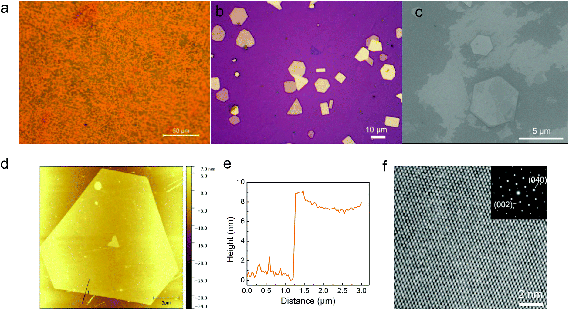 | ||
| Fig. 1 (a) Optical image of graphene-Mo2C grown on a Cu foil. (b) Optical image of graphene-Mo2C after transferred to the Si/SiO2 substrate. (c) SEM image of the graphene-Mo2C heterostructure. (d) AFM topography of the graphene-Mo2C heterostructure. (e) AFM cross-setional profile along the black line in (d). (f) HRTEM image of Mo2C showing the atomic structure. The inset shows the SAED result. | ||
In order to reveal the stability of the graphene–Mo2C heterostructure, the sample was annealed at 200 °C in ambient condition. Any difference in the heterostructure can be hardly seen from the optical images of the sample before (Fig. 2a) and after (Fig. 2b) annealing. Fig. 2c shows the Raman spectrum of the graphene–Mo2C heterostructure excited by a 633 nm laser. The peak of 149 cm−1 at the low frequency is the characteristic peak of Mo2C, and the peaks at 1580 cm−1 and 2700 cm−1 are consistent with the G-band and 2D-band of graphene, respectively.24,33 The optical absorption of the graphene–Mo2C heterostructure thin film in comparison with graphene was also investigated, as shown in Fig. 2d. We can see that the graphene–Mo2C heterostructure has an enhanced absorption over a wide wavelength range from 500 nm to 1800 nm, which is essential for broadband photodetection.
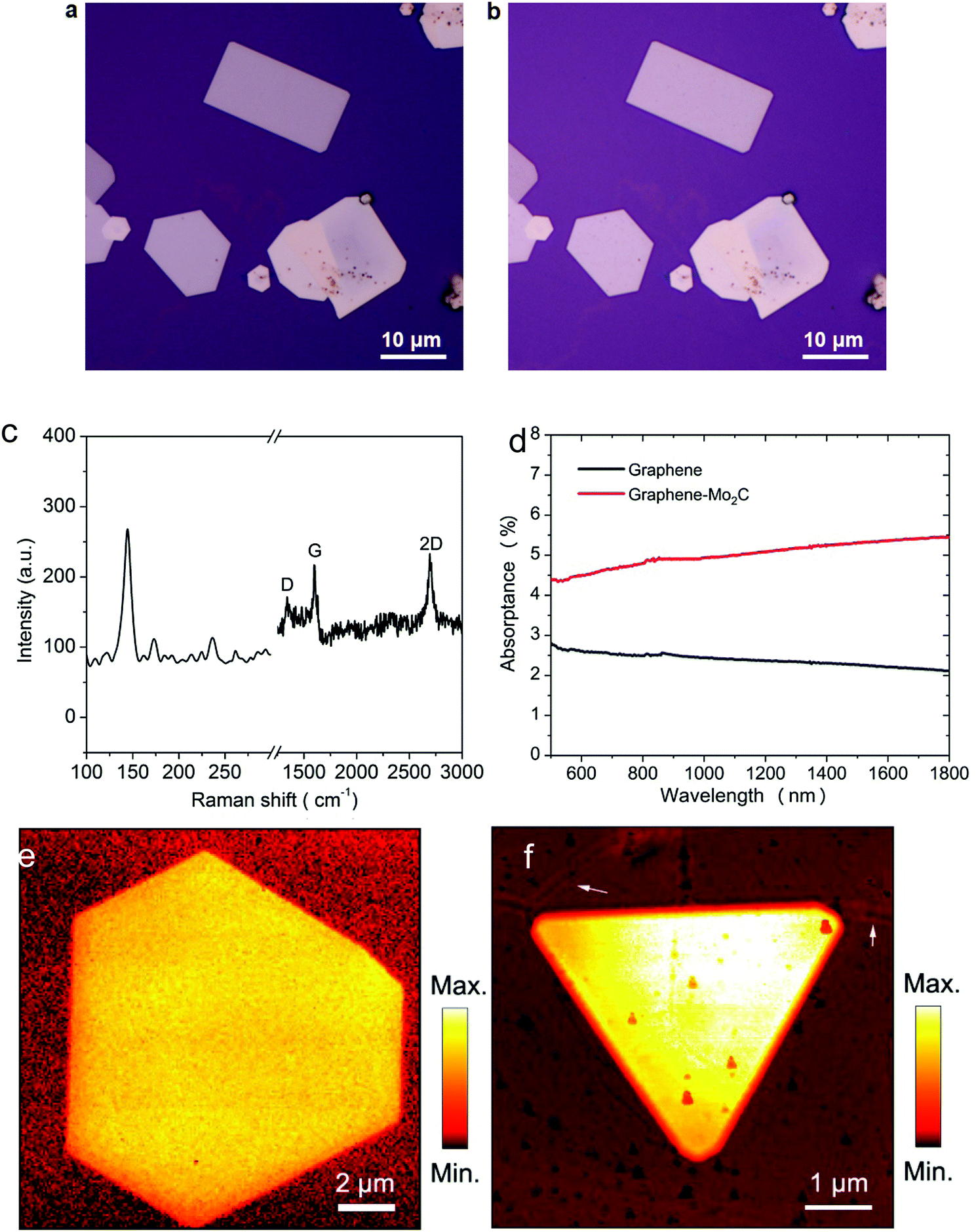 | ||
| Fig. 2 (a and b) Optical images of the graphene-Mo2C heterostructure before (a) and after (b) annealing at 200 °C in ambient conditions. (c) Raman spectrum of the graphene-Mo2C heterostructure with characteristic peaks of graphene and Mo2C. (d) The optical absorption property of the graphene-Mo2C heterostructure in comparison with that of graphene. (e) SNOM amplitude image of pure Mo2C. (f) SNOM amplitude image of the graphene-Mo2C heterostructure. The near-field amplitudes in (e) and (f) have been normalized to the substrates for comparison. The arrows in (f) indicate the plasmon fringes from the wrinkles or grain boundaries in graphene. | ||
A scattering-type scanning near-field optical microscope (s-SNOM) was used to investigate the photocarriers of the heterostructure, as shown in Fig. 2e and f. More measurement details are provided in the Experimental section. The near-field image that is excited by the mid-infrared laser at 10.8 μm is capable of mapping the free-carrier distribution in the graphene–Mo2C heterostructure and the pure Mo2C sheet. It is clearly seen that the Mo2C sheet on top of graphene looks brighter and has a few times higher near-field amplitude than the pure Mo2C flake, which indicates larger localized carrier density. More photocarriers in the graphene–Mo2C heterostructure compared to intrinsic Mo2C may result from the charge transfer between graphene and Mo2C, which underpins the performance enhancement for photodetection.
We first study the photodetection of the graphene–Mo2C heterostructure at the visible wavelengths, as presented in Fig. 3. The schematic of the graphene–Mo2C heterostructure photodetector device on Si/SiO2 is illustrated in Fig. 3a, and the optical image of a real device is shown in Fig. 3b. The graphene-Mo2C heterostructure was applied as the channel material with a channel length of 8 μm and a width of 10 μm, in which graphene is on top of the Mo2C sheets and gold electrodes are on top of graphene. As the Mo2C sheet in the channel area has a large size, both the electrodes are contacted with graphene and Mo2C sheet at the bottom. We proposed a schematic energy diagram to illustrate the movement of photoexcited carriers under illumination in the graphene–Mo2C heterostructure, as depicted in Fig. 3c. Graphene is a semi-metal and Mo2C is metallic. The work function of graphene is 4.6 eV,34 and the work function of Mo2C is 4.75 eV.35 While they are in contact, electrons will transfer from graphene to Mo2C according to the simulation of charge density difference (Fig. S1, ESI†) until their Fermi levels are aligned together. Consequently, a built-in electrical field is formed as a result of balancing carrier concentrations at the junction. The work function of the graphene–Mo2C heterostructure is calculated to be ∼4.71 eV (see Fig. S1, ESI†). Under illumination, both graphene and Mo2C can harvest incident light and generate photocarriers. With the help of the built-in electrical field in the heterostructure as well as external bias, the photocarriers are driven from Mo2C to graphene and then transferred to two electrodes, leading to enhanced photocurrent.
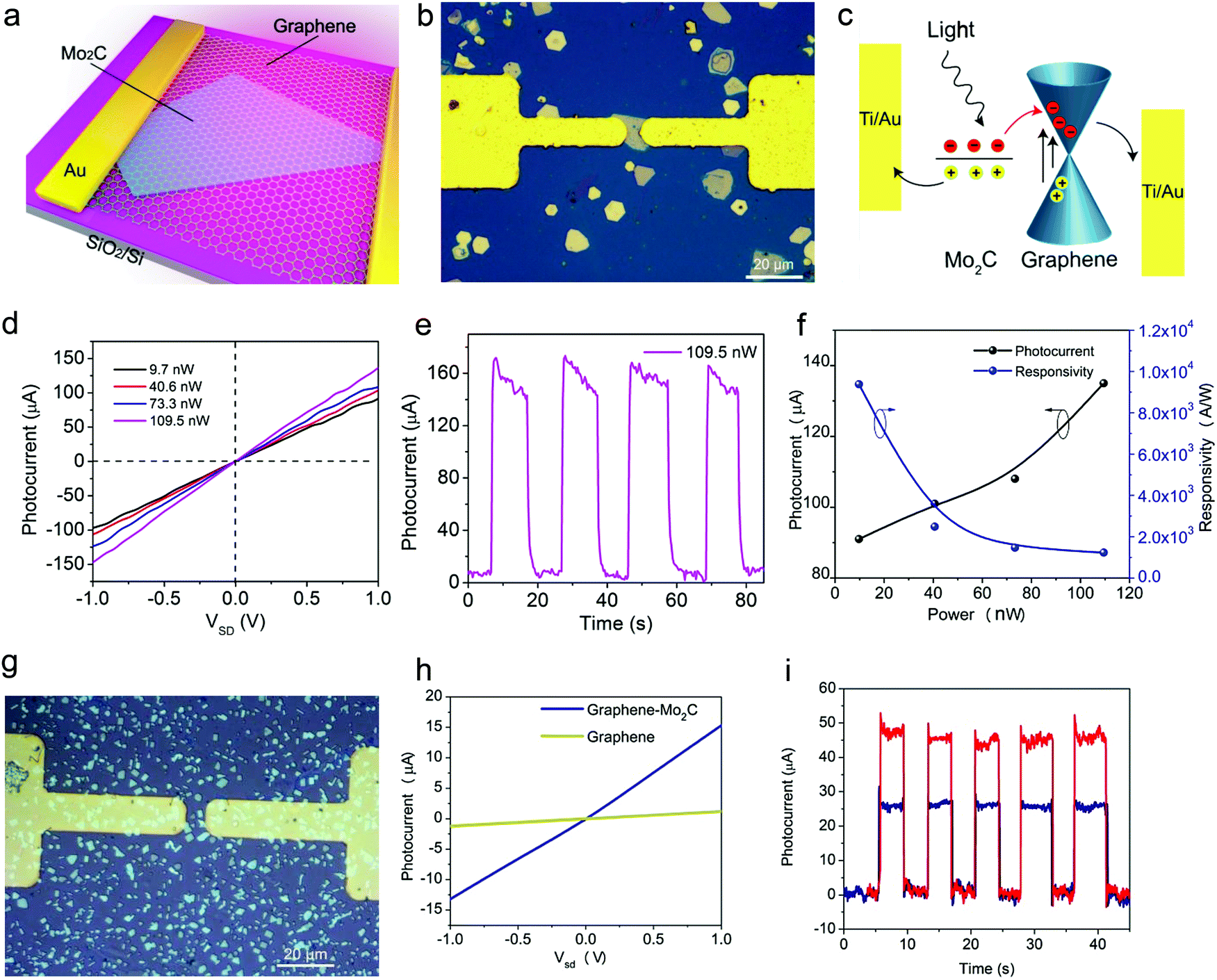 | ||
| Fig. 3 (a) Schematic of the graphene-Mo2C heterostructure photodetector device. (b) Optical image of the photodetector device on the Si/SiO2 substrate showing the heterostructure with a large piece of Mo2C sheet underneath graphene crossing the channel. (c) Band diagram of the graphene–Mo2C heterostructure under illumination showing the transferring of photoexcited carriers. (d) The I–V curves of the graphene–Mo2C device with large Mo2C sheet illuminated by 405 nm laser under different laser powers. (e) The time-dependent photocurrent curve of the graphene–Mo2C device with large Mo2C sheet. Vsd = 1 V. Laser power: 109.5 nW. (d) Photocurrent and responsivity of the graphene–Mo2C device with large Mo2C sheet as a function of laser powers at 405 nm. (g) Optical image of the photodetector device on the Si/SiO2 substrate showing a few small pieces of Mo2C sheets in the channel. (h) The I–V curve of graphene–Mo2C device with small Mo2C sheets illuminated by 635 nm laser under laser power of 300 nW. (i) The time-dependent photocurrent curve of the graphene–Mo2C device with small Mo2C sheets. Vsd = 1 V. Laser power: 400 nW (black trace) and 500 nW (red trace). | ||
Fig. 3d–f shows the photodetection results of the graphene–Mo2C heterostructure consisting of a larger piece of the Mo2C sheet. The photocurrent curves as a function of source-drain bias was measured under the illumination of 405 nm light at different incident powers, as presented in Fig. 3d. The photocurrent increases linearly as Vsd varies from −1 to 1 V, suggesting Ohm's contact between the heterostructure and electrodes. Larger photocurrent is observed at higher light power, and the photocurrent can be effectively turned on and off with a relatively fast response, as depicted in Fig. 3e. The power-dependent photocurrent and responsivity are plotted in Fig. 3f. The photocurrent increases nonlinearly, while the incident power increases beyond 70 nW, and the corresponding photoresponsivity decreases exponentially with increasing power. The highest responsivity of 9381.4 A W−1 is observed under the weakest light illumination (10 nW at 405 nm). Above 70 nW laser illumination, the responsivity reaches a state, and it reads as 1232.9 A W−1 at 110 nW.
To investigate the size effect of Mo2C sheet on the photodetection performance, we fabricated a photodetector device on the graphene–Mo2C heterostructure consisting of smaller pieces of Mo2C sheets (size: 1–2 μm), as shown in Fig. 3g. Fig. 3h presents photocurrent as a function of source–drain voltage under illumination at a 635 nm laser with a power of 300 nW, and the photocurrent of the heterostructure is about 23 times higher than that of a pure graphene device. Nevertheless, the photocurrent of this device (about 10 μA) is about ten times smaller than that of the device with a large piece of Mo2C sheet (∼100 μA, Fig. 3d) despite the difference in light power and wavelength. The time-dependent photocurrent curve was obtained under the illumination of 635 nm light using different laser power at fixed source–drain bias of 1 V, as shown in Fig. 3i. Similar to the above-mentioned observation, the graphene–Mo2C photodetector can be effectively switched on and off with a rise time of 5.4 ms, and the photocurrent increases from 27 μA to 47 μA, when the laser power increases from 400 nW to 500 nW. The responsivity is calculated to be 94 A W−1 at the laser power of 400 nW, which is also ten times smaller than that of the device with a large piece of Mo2C sheet (1232.9 A W−1 at 110 nW, Fig. 3f).
To further investigate the photodetection performance at the infrared range, we measured the heterostructure devices under the illumination of 1064 nm and 1550 nm lasers, as depicted in Fig. 4. For comparison, the devices consisting of both large Mo2C sheet and smaller pieces of Mo2C sheets have been studied. Fig. 4a and c show time-dependent photocurrent of the graphene-Mo2C device with a large single Mo2C sheet tested at 1064 nm and 1550 nm under different irradiation powers. The photocurrent can be turned on and off when the light is switched on and off, while larger light power gives higher photocurrent. As the thermal noise has an effect on the photocurrent, the photocurrent curve is not as straight as those measured at 405 nm and 635 nm. The photocurrent and responsivity as a function of illumination power are plotted in Fig. 4b and d. Similar power dependence to that in the visible range can be observed in infrared wavelengths. It is noteworthy to mention that the highest responsivity achieved is 9.2 A W−1 at 1064 nm and 6.9 A W−1 at 1550 nm, which is comparable to our previous report on other graphene heterostructures.36 The photodetector based on graphene and smaller pieces of Mo2C sheets was also measured at 1550 nm, and the results are shown in Fig. 4e and f. The trends of the power-dependent photocurrent and responsivity are similar to that of the device with graphene and large Mo2C sheet but at relative lower scale. In particular, at the power of 15 μW, we can get a responsivity of 0.4 A W−1, which is about 20 times smaller than that of the heterostructure device based on graphene and large Mo2C sheet, but about 260 times higher than pure graphene device (1.5 mA W−1).5,6 We also compared our results with similar heterostructure devices consisting of graphene and other materials, as shown in Table S1 (ESI†). Based on the above-mentioned comparisons, we can conclude that the heterostructure device consisting of graphene and large Mo2C sheet can deliver much better photodetection performance from visible to near-infrared wavelength ranges in terms of higher responsivity and shorter response time. This is because a large Mo2C sheet can absorb more light and generate more photoexcited carriers, which can also be effectively injected into graphene and collected by two electrodes more efficiently due to shorter transport pathway.
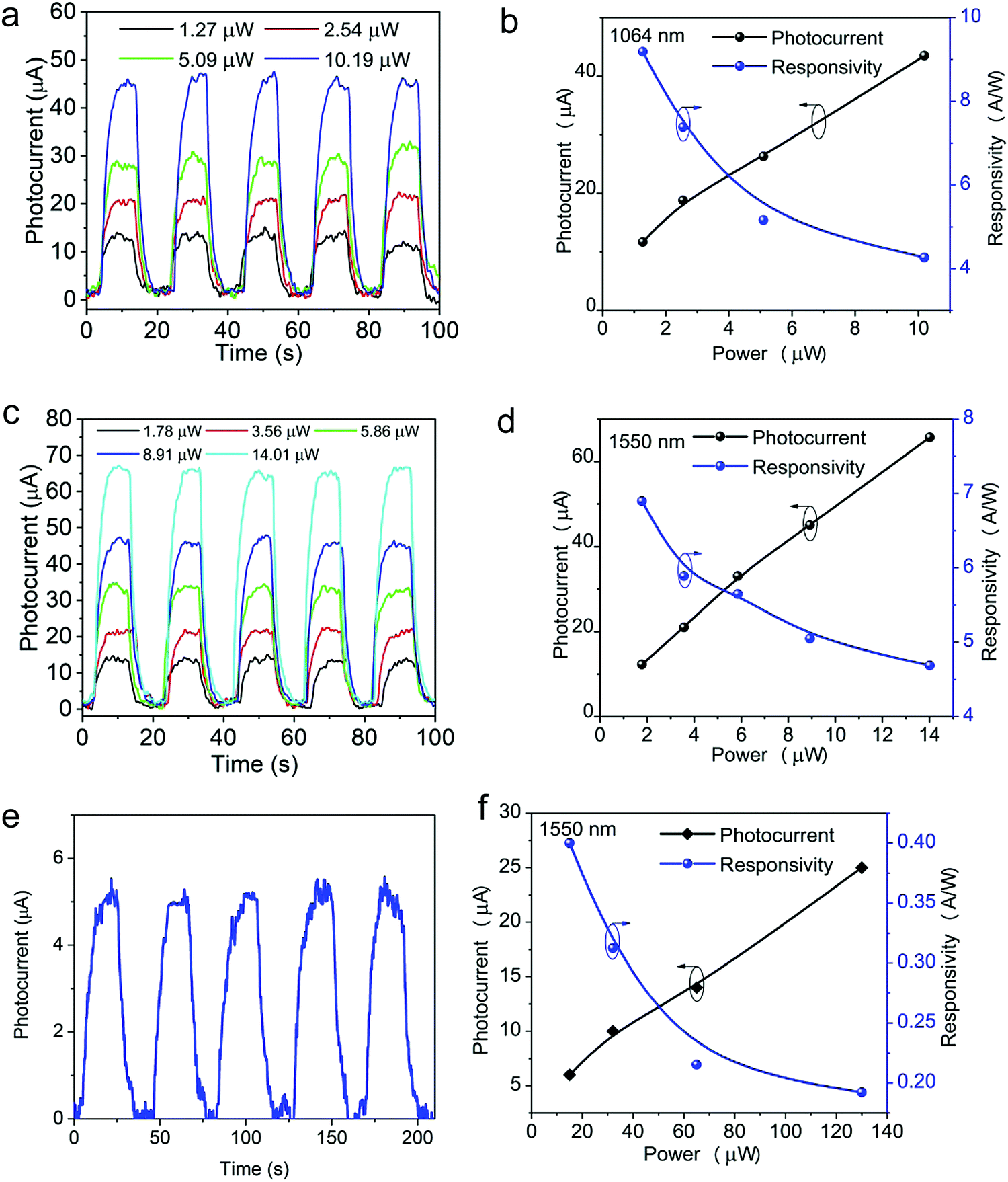 | ||
| Fig. 4 (a) Time dependent photocurrent of the graphene–Mo2C device with s large Mo2C sheet tested at 1064 nm under different irradiation powers. Source–drain bias: 1 V, zero gate voltage. (b) Photocurrent and responsivity as a function of laser powers at 1064 nm for graphene–Mo2C device with large Mo2C sheet. (c) Time dependent photocurrent of the graphene–Mo2C device with the large Mo2C sheet tested at 1550 nm under different irradiation powers. Source–drain bias: 1 V, zero gate voltage. (d) Photocurrent and responsivity as a function of laser powers at 1550 nm for the graphene–Mo2C device with the large Mo2C sheet. (e) Time-dependent photocurrent of the graphene–Mo2C device with small Mo2C sheets tested at 1550 nm under the irradiation power of 15 μW. (f) Photocurrent and responsivity as a function of laser powers at 1550 nm for the graphene–Mo2C device with small Mo2C sheets. | ||
Conclusions
In conclusion, we successfully demonstrated a highly responsive broadband photodetector based on the graphene–Mo2C heterostructure that operates from visible to near-infrared telecommunication wavelengths. Because of the semi-metallic nature of both graphene and Mo2C, the heterostructure has large photon absorption over a broad wavelength range. The construction of the vertical heterostructure allows an efficient transport of photoexcited carriers from Mo2C to graphene so as to be collected by the electrodes. The heterostructure device with a large Mo2C sheet exhibits not only broadband photodetection from the visible to telecommunication wavelengths, but also showed an ultrahigh photoresponsivity of 9381.4 A W−1 at 405 nm and relatively high responsivities at infrared wavelengths, i.e., 9.2 A W−1 at 1064 nm and 6.9 A W−1 at 1550 nm. The device is very durable as both materials have very good air stability. The demonstration of the unprecedented performance of the graphene–Mo2C heterostructure photodetector may find intriguing potential for practical applications such as in optical sensing, biological imaging and optical communication.Experimental section
CVD growth and transfer of graphene–Mo2C crystals
A monolayer graphene film was first grown on a Cu foil (Alfa Aesar, 99.5% purity, 10 μm thick) according to previous reports.37 Then, the foil was cut into 5 × 5 mm2 pieces and placed on top of a Mo foil (Alfa Aesar, 99.95% purity, 100 μm thick) of the same size. The graphene/Cu/Mo sample was then placed in a quartz tube of outer diameter 25 mm and inner diameter 22 mm to act as the growth substrate for Mo2C crystals. Subsequently, the graphene/Cu/Mo substrate was heated above 1085 °C in a horizontal tube furnace (Lindberg Bule M, TF55030C) under H2 (200 sccm). A small amount of CH4 (1.5 sccm) was then introduced into the reaction tube at ambient pressure to initiate the growth of 2D Mo2C crystals on a graphene film, which usually lasted for 2–50 min. The longer the growth time, the larger the size of the ultrathin Mo2C crystals. Finally, the sample was cooled down to room temperature at a cooling rate of 20–50 °C min−1 while maintaining the flow of CH4 at the same rate.A thin layer of poly (methyl methacrylate) (PMMA, weight-averaged molecular mass Mw = 600000, 4 wt% in ethyl lactate) was first spin-coated onto the surface of Mo2C/graphene samples at 5000 rpm for 1 min and cured at 180 °C for 30 min. The PMMA-coated samples were then immersed in a 0.2 M (NH4)2S2O8 solution at 70 °C for 10 min to etch away the Cu substrate. After that, the PMMA-coated Mo2C/graphene samples were transferred onto the SiO2/Si substrate. Finally, acetone was used to remove the PMMA layer and obtain the clean Mo2C/graphene heterostructure film. The synthesis and transfer process of graphene-Mo2C can also refer to previous report in ref. 30.
Characterizations of the graphene–Mo2C heterostructure
The surface morphologies of the graphene–Mo2C photodetectors were examined by SEM (Carl Zeiss, supra-55). The thicknesses of the graphene–Mo2C heterostructures were measured via AFM (Bruker, Dimension Icon). The Raman spectra were collected using a micro-Raman system (Horiba Jobin Yvon, LabRAM HR 800) with a 514 nm excitation laser. Near-field optical images were captured using a commercial scattering type SNOM (NeaSNOM, NeaSpec GmbH) setup with a CO2 laser (Edinburgh Instruments).Device fabrication and photoelectric measurements
UV lithography was conducted to define the device pattern, electron-beam evaporation was performed to deposit gold (Au) contacts with a thickness of 100 nm, and a lift-off technique was used to form the source and drain electrodes on top of graphene. For the electrical transport measurement, a direct current (DC) bias voltage (1 V) was applied to one Au contact (source), allowing the source–drain current (Isd) to flow through the graphene-BP heterostructure and reach the other Au contact (drain).Optoelectronic measurements of the graphene–Mo2C photodetector
The device characteristics measured at multiple wavelengths (405 nm, 635 nm, 1064 nm and 1550 nm) were performed by using a probe station (Cascade M150) equipped with a semiconductor property analyzer (Keithley 4200). All the measurements were performed at room temperature under ambient conditions.Author contributions
X. B. and T. S. contributed equally to this work. W. R., Q. B. and H. S. supervised the project. X. B. and T. S. planned and performed most of the experiments. C. X., S. L., J. G. and W. R. contributed to material synthesis and characterizations. Y. L., J. G., Y. Z., S. B. N., G. X. and S. L. contributed to device fabrication and photocurrent measurements. X. B., T. S., Y. L., W. R., Q. B. and H. S. analyzed the data and co-wrote the paper. All authors discussed the results and commented on the manuscript. All authors have approved the final version of the manuscript.Conflicts of interest
There are no conflicts to declare.Acknowledgements
We acknowledge the support from National Key Research & Development Program of China (No. 2016YFA0201902), the National Natural Science Foundation of China (No. 62022081, 61974099, 91733302, 61605073, and 61935017), Guangdong- Hong Kong-Macau Joint Laboratory (Grant no. 2019B121205001), the Shenzhen Nanshan District Pilotage Team Program (No. LHTD20170006), the Macau Science and Technology Development Fund (FDCT No. 0098/2020/A2, 0019/2019/AGJ, FDCT-091/2017/A2, and FDCT-014/2017/AMJ), Research Grants from University of Macau (MYRG2019-00055-IAPME), and Natural Science Foundation of Guangdong Province (Grant No. 2021A1515010694).Notes and references
- Q. Bao, H. Zhang, B. Wang, Z. Ni, C. H. Y. X. Lim, Y. Wang, D. Y. Tang and K. P. Loh, Nat. Photonics, 2011, 5, 411–415 CrossRef CAS.
- M. Liu, X. Yin, E. Ulin-Avila, B. Geng, T. Zentgraf, L. Ju, F. Wang and X. Zhang, Nature, 2011, 474, 64–67 CrossRef CAS PubMed.
- S. Bae, H. Kim, Y. Lee, X. Xu, J. S. Park, Y. Zheng, J. Balakrishnan, T. Lei, H. R. Kim and Y. I. Song, Nat. Nanotechnol., 2010, 5, 574–578 CrossRef CAS PubMed.
- N. M. Gabor, J. C. Song, Q. Ma, N. L. Nair, T. Taychatanapat, K. Watanabe, T. Taniguchi, L. S. Levitov and P. Jarillo-Herrero, Science, 2011, 334, 648–652 CrossRef CAS PubMed.
- T. Mueller, F. Xia and P. Avouris, Nat. Photonics, 2010, 4, 297–301 CrossRef CAS.
- F. Xia, T. Mueller, Y.-M. Lin, A. Valdes-Garcia and P. Avouris, Nat. Nanotechnol., 2009, 4, 839–843 CrossRef CAS PubMed.
- R. R. Nair, P. Blake, A. N. Grigorenko, K. S. Novoselov, T. J. Booth, T. Stauber, N. M. Peres and A. K. Geim, Science, 2008, 320, 1308 CrossRef CAS PubMed.
- K. I. Bolotin, K. J. Sikes, Z. Jiang, M. Klima, G. Fudenberg, J. Hone, P. Kim and H. L. Stormer, Solid State Commun., 2008, 146, 351–355 CrossRef CAS.
- S. Morozov, K. Novoselov, M. Katsnelson, F. Schedin, D. Elias, J. A. Jaszczak and A. Geim, Phys. Rev. Lett., 2008, 100, 016602 CrossRef CAS PubMed.
- F. H. Koppens, D. E. Chang and G. D. A. Fj, Nano Lett., 2011, 11, 3370–3377 CrossRef CAS PubMed.
- T. Echtermeyer, L. Britnell, P. Jasnos, A. Lombardo, R. Gorbachev, A. Grigorenko, A. Geim, A. C. Ferrari and K. Novoselov, Nat. Commun., 2011, 2, 1–5 Search PubMed.
- M. Furchi, A. Urich, A. Pospischil, G. Lilley, K. Unterrainer, H. Detz, P. Klang, A. M. Andrews, W. Schrenk and G. Strasser, Nano Lett., 2012, 12, 2773–2777 CrossRef CAS PubMed.
- A. Splendiani, L. Sun, Y. Zhang, T. Li, J. Kim, C.-Y. Chim, G. Galli and F. Wang, Nano Lett., 2010, 10, 1271–1275 CrossRef CAS PubMed.
- O. Lopez-Sanchez, D. Lembke, M. Kayci, A. Radenovic and A. Kis, Nat. Nanotechnol., 2013, 8, 497–501 CrossRef CAS PubMed.
- K. Roy, M. Padmanabhan, S. Goswami, T. P. Sai, G. Ramalingam, S. Raghavan and A. Ghosh, Nat. Nanotechnol., 2013, 8, 826–830 CrossRef CAS PubMed.
- A. Gao, E. Liu, M. Long, W. Zhou, Y. Wang, T. Xia, W. Hu, B. Wang and F. Miao, Appl. Phys. Lett., 2016, 108, 223501 CrossRef.
- K. Kam and B. Parkinson, J. Phys. Chem., 1982, 86, 463–467 CrossRef CAS.
- K. F. Mak, C. Lee, J. Hone, J. Shan and T. F. Heinz, Phys. Rev. Lett., 2010, 105, 136805 CrossRef PubMed.
- M. Naguib, O. Mashtalir, J. Carle, V. Presser, J. Lu, L. Hultman, Y. Gogotsi and M. W. Barsoum, ACS Nano, 2012, 6, 1322–1331 CrossRef CAS PubMed.
- M. Naguib, V. Mochalin, M. W. Barsoum and Y. Gogotsi, Adv. Mater., 2014, 26, 992–1005 CrossRef CAS PubMed.
- L. Toth, Transition metal carbides and nitrides, Elsevier, 2014 Search PubMed.
- N. Morton, B. James, G. Wostenholm, D. Pomfret, M. Davies and J. Dykins, J. Less-Common Met., 1971, 25, 97–106 CrossRef CAS.
- R. Willens, E. Buehler and B. Matthias, Phys. Rev., 1967, 159, 327 CrossRef CAS.
- H. Mu, M. Tuo, C. Xu, X. Bao, S. Xiao, T. Sun, L. Li, L. Zhao, S. Li and W. Ren, Opt. Mater. Express, 2019, 9, 3268–3276 CrossRef CAS.
- C. Xu, L. Wang, Z. Liu, L. Chen, J. Guo, N. Kang, X.-L. Ma, H.-M. Cheng and W. Ren, Nat. Mater., 2015, 14, 1135–1141 CrossRef CAS PubMed.
- W. Sun, X. Wang, J. Feng, T. Li, Y. Huan, J. Qiao, L. He and D. Ma, Nanotechnology, 2019, 30, 385601 CrossRef CAS PubMed.
- S. Chaitoglou, P. Tsipas, T. Speliotis, G. Kordas, A. Vavouliotis and A. Dimoulas, J. Cryst. Growth, 2018, 495, 46–53 CrossRef CAS.
- R. Deng, H. Zhang, Y. Zhang, Z. Chen, Y. Sui, X. Ge, Y. Liang, S. Hu, G. Yu and D. Jiang, Chin. Phys. B, 2017, 26, 067901 CrossRef.
- D. Geng, X. Zhao, Z. Chen, W. Sun, W. Fu, J. Chen, W. Liu, W. Zhou and K. P. Loh, Adv. Mater., 2017, 29, 1700072 CrossRef PubMed.
- C. Xu, S. Song, Z. Liu, L. Chen, L. Wang, D. Fan, N. Kang, X. Ma, H.-M. Cheng and W. Ren, ACS Nano, 2017, 11, 5906–5914 CrossRef CAS PubMed.
- Z. Kang, Z. Zheng, H. Wei, Z. Zhang, X. Tan, L. Xiong, T. Zhai and Y. Gao, Sensors, 2019, 19, 1099 CrossRef CAS PubMed.
- Y. Fan, C. Xu, X. Liu, C. Ma, Y. Yin, H.-M. Cheng, W. Ren and X. Li, NPG Asia Mater., 2020, 12, 1–9 CrossRef.
- A. C. Ferrari, J. C. Meyer, V. Scardaci, C. Casiraghi, M. Lazzeri, F. Mauri, S. Piscanec, D. Jiang, K. S. Novoselov and S. Roth, Phys. Rev. Lett., 2006, 97, 187401 CrossRef CAS PubMed.
- Y. Shi, K. K. Kim, A. Reina, M. Hofmann, L.-J. Li and J. Kong, ACS Nano, 2010, 4, 2689–2694 CrossRef CAS PubMed.
- R. Wilson and W. McKee, J. Appl. Phys., 1967, 38, 1716–1718 CrossRef CAS.
- T. Sun, Y. Wang, W. Yu, Y. Wang, Z. Dai, Z. Liu, B. N. Shivananju, Y. Zhang, K. Fu and B. Shabbir, Small, 2017, 13, 1701881 CrossRef PubMed.
- Y. Zhu, S. Murali, W. Cai, X. Li, J. W. Suk, J. R. Potts and R. S. Ruoff, Adv. Mater., 2010, 22, 3906–3924 CrossRef CAS PubMed.
Footnote |
| † Electronic supplementary information (ESI) available. See DOI: 10.1039/d1cp03536c |
| This journal is © the Owner Societies 2021 |