
 Open Access Article
 This Open Access Article is licensed under a
 Creative Commons Attribution 3.0 Unported Licence
Refractive index sensing in a monolithic micro-optofluidic lithium niobate chip†
Daniel Nwatu *,
Sergiy Suntsov,
Detlef Kip and
Kore Hasse
*,
Sergiy Suntsov,
Detlef Kip and
Kore Hasse
Faculty of Electrical Engineering, Helmut Schmidt University, 22043 Hamburg, Germany. E-mail: nwatudaniel95@gmail.com
First published on 1st July 2025
Abstract
Lithium niobate is an outstanding material for the realization of fully integrated lab on a chip devices due to its variety of physical properties, such as high electro-optic, acousto-optic, pyro-electric, and nonlinear coefficients, which enable multiple functionalities. As a proof of principle for a monolithic optofluidic sensor, we report the fabrication of a refractive index sensor consisting of a femtosecond laser written waveguide crossing a microfluidic channel, which was fabricated in a lithium niobate sample. The microchannel was created by selective etching of a femtosecond laser inscribed structure and the surfaces of the etched channel were smoothed by subsequent annealing. Sensitivity and accuracy of the sensor were determined by refractive index measurements of sucrose solutions with different concentrations and the temperature dependency was investigated with an air-filled channel. The Fabry–Pérot interference spectrum recorded in reflection shows a high contrast of 24 dB, which indicates good optical quality of the cavity. Refractive index steps of 10−3 were measured with an accuracy of 8.5 × 10⁻⁵ and a sensitivity of 1215 nm RIU−1 at a wavelength of 1554 nm. A very low repeatability error was determined by multiple measurements under stabilized temperature conditions.
Introduction
In lab on a chip, the integration of optical probing is still a challenge today, and leads to limitations in the integration of multiple functions, and thus the miniaturization of devices.1 In particular, the optical detection and control of fluids and their constituents, e.g., particles such as cells, are often realized externally with bulky equipment.2 A material that has all the physical properties required to integrate these functions on a single platform could help overcome the current limitations. Most of the common platforms like glass or PDMS3 do not offer these properties, or the surface properties such as the roughness of the microchannels fabricated in these materials limit the combination with optical elements such as integrated waveguides. However, lithium niobate (LiNbO3, LN) is an electro-optic, acousto-optic, piezo-electric, pyro-electric, and nonlinear optical crystal. It has a wide transparency range from 340 nm to 5.500 nm, and also exhibits high mechanical stability (compared to, e.g., PDMS), and could serve as an alternative versatile platform.2Due to the above properties, LN could enable the integration of a tremendous number of applications. They range from RI sensing (selectively etched Fabry–Pérot (FP) cavities) over fluorescence spectroscopic detection and analysis (waveguides, integrated frequency conversion, electro-optic modulation) to active (using surface acoustic wave (SAW) based micropumps4) and passive cell sorting and manipulation or mixing of fluids5 in a single platform. This multifunctionality is illustrated in a vision of a future integrated LN device in Fig. 1. With such a monolithic micro-optofluidic LN chip, several fluids could be mixed using SAW micropumps and a meandric microchannel structure. The fluids could be further analysed using a crossing waveguide for RI sensing. Intersecting waveguides forming optical tweezers could be used for particle trapping, and the fluid or constituents could be further analysed spectroscopically, after excitation with light from another crossing waveguide, by a fully integrated spectrometer unit. Particles could be sorted in a SAW-based particle sorter and afterwards counted using particle counters consisting of waveguides crossing the different outlet channels for each species forming a light barrier.
 | ||
| Fig. 1 Vision of a future multifunctional microfluidic LN platform. | ||
Using a non-monolithic approach, several micro-optofluidic sensors have been demonstrated already in LN. For example, devices for measuring the pH value in microchannels by absorption,1 real-time droplet sensors,2,6 flowmeters,7 and droplet manipulation by photo-induced electric field effects have been realized.8 However, as mentioned above, none of these demonstrations were realized completely monolithically: all required covers that were glued onto the microfluidic channels, as the channels were fabricated either by ablation or precision dicing on the top of the sample. In contrast, selective etching of structures inscribed with femtosecond (fs) lasers in transparent materials such as glasses or crystals enables the fabrication of microchannels that are buried in the sample volume, and thus are completely sealed. This was demonstrated with an RI sensor, based on a whispering gallery mode resonator in a microfluidic channel in glass,9 and a cell separator based on selectively etched microchannels in YAG.5
The method of selective etching of structures inscribed with an fs laser was recently demonstrated in LN.10 For selective etching, structures are inscribed in the volume of transparent LN crystals. It is possible to inscribe these structures without damaging the surrounding material by nonlinear absorption of a strongly focused laser pulse. Due to the intensity dependence of the absorption mechanism, the modification is limited to the focal volume. It is known from μ-fluorescence imaging of the fs laser modified areas that atomic bonds are distorted and a certain disorder is induced in the crystal lattice.11 If the laser modification results in weakening of the bonds, the modified material can be dissolved more easily with a suitable etching agent than the pristine material so that hollow microchannels can be fabricated by selective etching. It should be noted that this recently discovered method allows fabrication of the microchannels even just a few micrometres below the sample surface in LN. Consequently, it should be possible to achieve strong penetration of SAWs into these microchannels. This could enable pumping liquids or sorting particles inside the channels, which is not possible to realize monolithically in fully sealed microchannels with any other method. Furthermore, a technique to smooth the selectively etched surfaces to an average roughness in the range of a few nanometres by post-etching annealing was discovered.12 It enables the integration of the selectively etched channels with fs laser inscribed waveguides at an acceptable low loss level. The use of these newly discovered methods in LN can thus enable a higher level of integration than the current status.
Refractive index (RI) sensing plays a crucial role as a non-invasive, label-free and therefore safe and low-cost method in many areas like biomedicine, molecular sensing in environmental monitoring, food testing and the security sector.13 To date, numerous RI sensors based on fibers14 and plasmonic metamaterials and metasurfaces,13 as well as sensors consisting of glass capillaries15 and whispering gallery mode resonator-based sensors9 have been realized. With these RI sensors, sensitivities in the range of 2032% per RIU14 and detection limits of 10−4 to 10−7 RIU16 and down to the single molecule level13 have been achieved. In particular, integrated RI sensors, which incorporate microfluidic channels, can be compact, robust, and easy-to-transport instruments with comparably low manufacturing costs.9 Including both optical probing and microfluidic channels, RI sensors thus resemble typical integrated micro-optofluidic devices.
To test the concept, we have fabricated an RI sensor in LN that combines an fs laser written waveguide with a selectively etched and annealed microchannel, forming an FP cavity. Using sucrose solutions of different concentration levels, the sensor is characterized by its ability to measure small RI changes. Additionally, the temperature dependence of the sensor and the repeatability of RI measurements were investigated. The device shows the potential of combining fs laser inscription and selective etching with the unique physical properties of LN and thus represents a milestone on the way to multifunctional micro-optofluidic platforms as sketched in Fig. 1.
Experimental
The design of the RI sensor is uncomplicated, consisting of a waveguide crossing a microchannel as sketched in Fig. 2(a). The microchannel that crosses the waveguide serves as a FP cavity whose reflectivity changes with the RI of the transported fluid. Selective etching of the microchannel and fs laser inscription of the waveguide are described below. Afterwards, the characterization method of the RI sensor is explained. | ||
| Fig. 2 Sketch of the RI sensor. a) Schematic visualizing how the microchannel structure was inscribed. b) Used scan technique (see text). | ||
Microfluidic channel fabrication
The microchannel structure is inscribed into the crystal volume using a 1 MHz repetition rate laser oscillator (Ekspla Femtolux 3) with a maximum average power of 3 W, a central wavelength of 1030 nm, and a pulse duration of 300 fs. The beam, with a pulse energy of 140 nJ, was polarized perpendicular to the writing direction and focused 220 μm deep into a 10 × 10 × 1 mm3 thick x-cut LN sample through an aspheric lens (f = 4.5 mm, NA = 0.55).The focus was translated at a scan speed of 10 mm s−1, 4 mm along the optical (z) axis 48 times, making 2 μm shifts along the y-direction after every track, as sketched in Fig. 2(b). Repeating this procedure, 12 horizontal layers were vertically stacked with a separation of approximately 10 μm to form a modified rectangular region 4 mm in length with a 95 × 142 μm2 cross section. At each end of the main channel structure, the focus was moved up layer by layer, similarly to the writing process of the main channel, to form vertical modifications with cross sections of 100 × 100 μm2 for inlet and outlet channels. The structure was inscribed starting from the bottom and translating the focus upwards, so that the modifications for the inlet and outlet ended at the surface, thus allowing the etching solution to enter the modified region directly from the ablated spot. This laser modified region was completely removed in 40% hydrofluoric acid (HF) at room temperature after 4 weeks of etching. Although this fabrication time is relatively long compared to that of other techniques such as precision dicing, this method is still viable for commercialization. Samples can be fabricated in parallel at the same time with high reproducibility. Only a minimal amount of energy and manpower is required for the etching process.
To smooth the sidewalls, the sample with the selectively etched channel was annealed for 60 hours at 1060 °C. The objective was to reduce the surface roughness as much as possible and at the same time maintain plane parallel channel sidewalls, to enable the FP effect for the RI measurement. The annealing process and its effects on microchannel shape and roughness are described in ref. 12. Accordingly, the applied annealing procedure should result in a sidewall roughness of 25 nm on the +y-plane and 12 nm on the −y-plane, while maintaining plane parallel sidewalls.
To demonstrate the flexibility of the selective etching process to fabricate almost arbitrarily shaped hollow microstructures in the volume of LN, several curved and crossing structures were inscribed and selectively etched under the same conditions as the microchannel of the RI sensor.
Waveguide inscription
The waveguide crossing the channel was fabricated by direct fs laser inscription using a multi-line technique as described in ref. 17. This means that 20 single tracks were inscribed at a speed of 20 mm s−1, with a pulse energy of 35 nJ and a distance of 0.4 μm from each other to form a rectangular 9.6 × 9.5 μm2 cross section. First, as a reference, waveguides were inscribed that did not cross any microchannel. These waveguides were characterized by transmission measurements at a wavelength of 1550 nm with respect to propagation losses, and the profile of the guided mode was captured.After that, waveguides intersecting the microchannel at a half height (i.e. 140 μm below the surface) were inscribed along the y-axis of the crystal, perpendicular to the microchannel, as sketched in Fig. 2(a). To minimize the influence of FP interference from the resonator formed by the LN sample itself, its facets (initially perpendicular to the waveguides) were cut at an angle of 6° to the xz-plane of the crystal.
Characterization using sucrose solutions
To characterize the fabricated RI sensor, a broadband light source from a fiber-coupled sensor interrogator (Micron Optics Si155) was coupled into the waveguide using a focusing lens. The interrogator has an output power of 0.25 mW, a resolution of 8 pm, a repeatability of ±1 pm, and a spectral range of (1460–1620) nm. The FP intensity modulation caused by the interference in the etched channel was recorded in reflection. The exact position of a reflection minimum in the spectra was analyzed by fitting a parabola around the minimum in question. With this method, a spectral resolution of approximately 0.2 pm, which is substantially higher than the 8 pm resolution of the interrogator itself, was achieved. Six distinct aqueous sucrose solutions with sucrose concentrations of 0.000%, 0.697%, 1.392%, 2.083%, 2.769%, and 3.453% (corresponding to 10−3 RI steps) were prepared to evaluate the sensitivity. The solutions were carefully mixed to ensure complete sucrose dissolution and homogeneous concentration distribution.Using a Gilson Pipetman μ-pipette, twenty microliter droplets of each solution were inserted into an inlet of the microchannel. The fluid was drawn into the microchannel by capillary forces. The process of continuous filling of the channel was observed visually, noting the slight change in color caused by the difference between the RI of the liquid and that of air. To determine the temperature dependence, reflection spectra were measured with an air-filled microchannel using a temperature range from 20 °C to 110 °C with measurements taken at 5 °C increments. For this purpose, the sample was mounted on a heatable sample holder. Every time the temperature was raised, the measurement was only taken after a few minutes once a thermal equilibrium was reached.
Finally, to evaluate the repeatability of the RI measurement, the reflection spectrum of the microchannel filled with deionized (DI) water was recorded 100 times over a time span of two hours. To account for a potential temperature-induced drift in the reflection minimum near 1550 nm, the ambient temperature was monitored using a precision thermometer (Anton Paar, MKT 50) with a resolution of 0.001 °C. The thermometer was placed in air in the immediate vicinity of the sample, which in turn was placed on a small aluminum block.
Results and discussion
Before selective etching, the fs laser inscribed channel structure was inspected under a microscope. Cross sectional images are shown in Fig. 3. The material modifications are smooth and homogeneous without visible cracks. Only the shading of the main channel structure is noted by a slight lightening on the bottom as depicted in Fig. 3(a). This is caused by the increase of the focal displacement, and thus the focal volume, due to an increase of spherical aberration with increasing writing depth. Thus, deeper below the surface, the material modification would be slightly larger in size but also weaker. The dark rectangular area on each side of the main channel structure in Fig. 3(b), shown with higher magnification in Fig. 3(c), is the ablated part at the surface. This is where the vertical inlet and outlet structure ends, so that the acid can directly enter the modified region. | ||
| Fig. 3 Microscope images of fs laser inscribed modification for selective etching of the microchannels: a) cross section, b) top view and c) zoomed in view of an outlet. | ||
Different cross-sectional microscope images of the selectively etched and annealed channel structure are shown in Fig. 4. Due to the high etching selectivity of up to 9000 along the z-axis,10 the 4 mm long etched channel in Fig. 4(a) and (b) has a perfectly rectangular cross section of 102 × 143 μm2, just like the outlets with a cross section of 102 × 120 μm2. The top view in Fig. 4(a) shows dark lines connected to the inlet and outlet channels at an angle of ≈45°. These lines are cracks that were induced by a too high energy load per volume during fs laser inscription but were not visible on the microscope image of the inscribed structure. They were only found after etching and annealing, since etching can increase the size of the crack. These cracks could be avoided by, e.g., reducing the pulse energy or increasing the vertical separation of the tracks, thus reducing the stress induced in the material by the fs laser. Fig. 4(c) shows the cross section of the main channel with the waveguide inscribed across the channel sidewalls after annealing. The location of the waveguides is depicted by red crosses in Fig. 4(b).
 | ||
| Fig. 4 Microscope images of cross sections of selectively etched channels. a) Top view, b) front view along the waveguide, and c) cross-sectional view with the attached fs laser written waveguides. The position of the waveguides is marked with red crosses in b). | ||
After annealing, the selectively etched channel was smooth with plane parallel sidewalls, as can be seen in Fig. 4(c). The initial surface roughness of the sample itself was determined to be ≤1 nm with a laser scanning microscope (Keyence VK-X3000), with a resolution of 1 nm. Selective etching produced a higher roughness of 20 nm. However, after subsequent annealing, a roughness of 4 nm was measured again.
After completing the annealing process, the waveguides were inscribed by translating the focus perpendicular to the channel and directly crossing it without laser beam interruption. Thus, the waveguides ended directly on the channel sidewalls. Since the ablation threshold is lower than the material modification threshold for fs laser structuring, one might expect ablation on the channel sidewalls. However, no ablation at the channel sidewalls was observed in the present experiments. In Fig. 4(b), the positions of the waveguides crossing the channel are marked with red crosses because the waveguide cross section is too small and the modification is too weak to be visible in the microscope image.
The waveguide cross section at a higher magnification and the guided mode profile are shown in Fig. 5. The material modification induced by the laser is very weak in the region of positive RI changes, where the light would be guided inside the modified region (type 1 waveguide18). The guided mode was measured at the outcoupling side, after the light passed the microchannel. It is an almost perfectly circular Gaussian mode with a beam radius of w0 = 7.7 μm, although the microscope image of the waveguide cross section shows a rectangular modification. Extraordinarily polarized light (TE modes) is guided with a propagation loss of 1.5 dB cm−1 inside the reference sample without the microchannel. Insertion losses of the waveguide crossing the microchannel were somewhat difficult to estimate because of the modulation due to the etalon effect of the cavity. Therefore, the Q-factor (λ/Δλ) was estimated for all minima. Quality factors of 1.9 × 10³ for the air-filled cavity and 9.6 × 10² for the water-filled cavity were obtained, similar to typical Q-factors of fiber-optic FP sensors.
 | ||
| Fig. 5 Microscope image of the waveguide cross section (left) and recorded intensity profile of the guided mode (right). | ||
Nevertheless, the modulation of the reflection spectrum (cf. Fig. 6(a)) shows a high contrast of 24 dB at around 1550 nm for an air-filled cavity, indicating smoothness and flatness of the channel sidewalls. Due to the high refractive index of LN, such a sensor is also advantageous for measurements of analytes with high RI in the 1.4–1.7 range. For this range, PDMS or glass-based sensors have poor visibility of FP fringes and thus low Q-factors. The modulation depth for the post-etching annealed resonator achieved here is in the same range as that of other sensitive FP sensors, which are around 15 to 26 dB.19 From the modulation period, the optical path length (the width of the microchannel) was calculated to be 102.2 μm. This value is in good agreement with the value of 102.0 μm measured from the microscope image of the cross section of the channel.
 | ||
| Fig. 6 a) Reflection spectrum of the microchannel FP resonator filled with air in the range of 1460–1620 nm. b) FP spectra for six sucrose solutions (inset shows concentrations) at around 1554 nm, and c) wavelength at minima vs. RI change. The red dashed line is a linear fit to the data. | ||
Fig. 6(b) shows the reflection spectra for six solutions, exhibiting an average wavelength shift of 1.215 nm per 10−3 RI change, corresponding to a sensor sensitivity of 1215 nm RIU−1. This sensitivity corresponds to the slope of the linear fit to the experimental data points shown in Fig. 6(c). There, the centre wavelength of the observed minima is plotted against the relative RI change. The measurement accuracy for the 10−3 RI steps investigated was determined to be ±8.5 × 10⁻⁵. It is well known that there is an RI variation with the temperature of both LN and liquids due to the thermo-optic effect (TOC).20,21 The RI change and the thermal expansion of LN, which could both influence the measurement accuracy, have to be taken into account.
For this reason, the temperature dependence of the RI measurement was investigated as described above. The results are depicted in Fig. 7, where the position of one minimum is plotted against temperature. This graph shows that the shift of the minimum is nearly linear with a slope of +0.020 nm °C−1 within the range of 25 °C to 55 °C. The expected sensitivity can be calculated as Δλ/ΔT = λ·α, since ΔL/L = Δλ/λ and α = ΔL/(LΔT).22 In these equations, α = 14.2 × 10⁻⁶ K−1 is the thermal expansion coefficient (TEC) of LN perpendicular to the optical c-axis,23 L is the length of the cavity, i.e. the microchannel width, and T is the temperature. The resulting theoretically calculated thermal sensitivity is +0.021 nm °C−1, which is in good agreement with the experimentally determined value of +0.020 nm °C−1. The change of the RI of air in the channel is very small within the investigated temperature range and can therefore be neglected.
 | ||
| Fig. 7 Temperature dependence of the microchannel RI sensor. The shift of the minimum located at 1547 nm for the air-filled cavity is plotted against the temperature. | ||
For the microchannel filled with an aqueous solution, the obtained thermal sensitivity has to be multiplied by the RI of the solution, giving a value of +0.027 nm °C−1. In addition, thermal sensitivity caused by the TOC of the solution must also be taken into account. The TOC of water is negative and has a value of −1.10 × 10⁻⁴ RIU °C−1 at 25 °C,21 which results in a thermal sensitivity of −0.133 nm °C−1. Thus, at room temperature, the overall thermal sensitivity would be dominated by the contribution of the TOC of the solution. As a result, the experimental RI measurement error of ±8.5 × 10⁻⁵ RIU could easily be caused by temperature fluctuations in the laboratory below 1 °C, which is not unusual for a one-hour long experiment. Nevertheless, the obtained accuracy is in the range of existing RI sensors.19 It could be further improved through temperature stabilization or by measuring the RI of a known fluid as a reference to correct the shift in the results.
Above 55 °C, the wavelength shift exhibits a super-linear dependence on temperature and can be better fitted with a quadratic function (see the red dashed line in Fig. 7). At 110 °C, the highest temperature applied, the waveguide mode became unstable. This instability might be caused by some temperature-induced RI changes that partially compensate the RI increase caused by the fs laser inscription. However, most biomedical optofluidic applications would not require such high temperatures, as most proteins and enzymes begin to denature at temperatures above 40 °C.
Even if the sensor cannot measure the RI independently of the temperature, this functionality can be realized by cutting only one facet of the LN crystal at an angle to the xz-plane, and the other side with a waveguide end face of 90° to form a second FP cavity. When the length of this LN cavity differs from the microchannel width, both cavities' resonance peaks can be clearly separated in the Fourier domain. With the known TEC and TOC of LN, the temperature can be obtained as done in ref. 24.
In order to evaluate the repeatability, 100 spectra were subsequently recorded with DI water as the analyte. Fig. 8 presents the extracted minima positions. A linear fit to these points shows that the wavelength position of the minima drifts over time by −0.020 nm, with a standard deviation of 4.5 pm around the fit line.
 | ||
| Fig. 8 Wavelength minima of the fitted spectrum for 100 repeated measurements taken over a time span of 2 hours. The red dashed line is a linear fit to the extracted minima position. | ||
Both the effect of the TOC of DI water (STOC = −0.133 nm °C−1) and the measured thermal sensitivity of the sensor itself (SSens = +0.027 nm °C−1) can explain the observed drift Δλ = −0.020 nm. It can be concluded that it corresponds to an estimated effective temperature increase of ΔTeff = Δλ/(STOC + SSens) = 0.19 °C in the analyte during the two-hour measurement span. In comparison, the measured temperature increase close to the sample in air during the same time frame was ΔTmeas = 0.25 °C, which is 0.06 °C higher than that inferred from the spectral drift in Fig. 8. This discrepancy can be attributed to a slight inertia in heat transport, which means that the metal holder for the sample only follows the heating of the surrounding air with a certain time delay. This means that its actual temperature lags slightly behind the ambient air. These results demonstrate that under stabilized temperature conditions, our sensor can reliably detect RI changes with a precision of 4.5 pm/(1.215 nm RIU−1) = 3.7 × 10⁻⁶ RIU.
Finally, in Fig. 9 some selectively etched microchannels with curved and crossing geometries are shown. All basic elements of the microfluidic channels can be fabricated with very high aspect ratios of length (>1 mm) to diameter (≈5 μm). The curved, intersecting, and y-branch channels were selectively etched from fs laser inscribed single line structures, and thus their diameter is roughly 5 μm. The vertical channel of the crossing structure is thinner in the middle. This can be explained by the lower etching selectivity along the y-axis of the crystal, compared to the selective etching along the z-axis. Due to the higher etch rate of the material modified with the fs laser, this taper disappears when exposing the structure to the acid for additional time after the channel has been completely etched. During this additional time, the acid can flow through the channel. This leads to straight sidewalls of the channels as visible on the T-junction channel. However, this process also leads to a slight increase of the width of the channel along its entire length, which needs to be considered during fs laser inscription when a certain width of a channel is targeted.
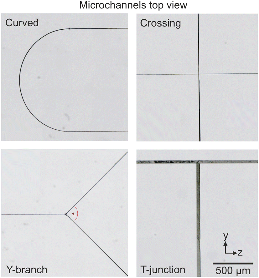 | ||
| Fig. 9 Curved and crossing selectively etched microchannels fabricated in LN. The scale and coordinate system with respect to the crystal axes hold for all images. | ||
Conclusions
The monolithic integration of the presented micro-optofluidic FP interference-based RI index sensor in LN offers the advantage of integrating the crystal's multifunctional properties with microfluidic circuits in a monolithic sample. This becomes feasible using the method of selective etching of fs laser inscribed structures in the sample volume, which was recently discovered for LN. With this method, all basic elements of microfluidic channels, such as curves and crossings, can be fabricated. Subsequent annealing reduces the roughness of the etched surfaces to optical-grade. It allows the integration of additional functions for analysis through more sophisticated optical elements, such as spectrometers and waveguides for particle excitation and trapping, interferometers, etc. Combining this method with the unique properties of LN can enable the integration of various functionalities in a compact and robust sample. For example, particle trapping using photo-induced electric fields,25 nano-pipetting using the pyro-electric effect,26 or usage of the photorefractive effect for red blood cell imaging27 as well as SAW-based micropumps for fluid and particle testing and manipulation, can be realized. This sample then would also contain the above mentioned microchannels and other hollow structures like reaction chambers as well as optical elements. In this way, a higher level of miniaturization can be reached, because the flow control in the microchannels and the optical probing can be integrated on the platform instead of using bulky external instruments. For this reason, we are convinced that our device represents a milestone towards more compact LN-based multifunctional micro-optofluidics.Data availability
The data supporting this article have been included as part of the ESI.†Author contributions
Conceptualization: K. H., D. K.; data curation: D. N., S. S.; formal analysis: D. N., S. S.; funding acquisition: K. H., D. K.; investigation: D. N.; project administration: K. H., D. K.; validation: K. H., S. S., D. K.; visualization: D. N.; writing – original draft: D. N.; writing – review and editing: K. H., S. S., D. K.Conflicts of interest
The authors declare no conflicts of interest.References
- R. Zamboni, A. Zaltron, E. Izzo, G. Bottaro, D. Ferraro and C. Sada, Sensors, 2020, 20, 5366 CrossRef CAS PubMed.
- G. Bettella, R. Zamboni, G. Pozza, A. Zaltron, C. Montevecchi, M. Pierno, G. Mistura, C. Sada, L. Gauthier-Manuel and M. Chauvet, Sens. Actuators, B, 2019, 282, 391–398 CrossRef CAS.
- C. Li, G. Bai, Y. Zhang, M. Zhang and A. Jian, Micromachines, 2018, 9, 1–10 CrossRef.
- M. Stringer, Z. Zeng, X. Zhang, Y. Chai, W. Li, J. Zhang, H. Ong, D. Liang, J. Dong, Y. Li, Y. Fu and X. Yang, Appl. Phys. Rev., 2023, 10, 011315 CAS.
- D. Choudhury, W. T. Ramsay, R. Kiss, N. A. Willoughby, L. Paterson and A. K. Kar, Lab Chip, 2012, 12, 948–953 RSC.
- R. Zamboni, A. Zaltron, M. Chauvet and C. Sada, Sci. Rep., 2021, 11, 17987 CrossRef CAS PubMed.
- R. Zamboni, L. Gauthier-Manuel, A. Zaltron, L. Lucchetti, M. Chauvet and C. Sada, Opt. Express, 2023, 31, 28423–28436 CrossRef CAS.
- G. Bragato, A. Zaltron, M. Zanardi, R. Zamboni, M. De Ros and C. Sada, Adv. Mater. Interfaces, 2024, 11, 2301008 CrossRef CAS.
- L. Kelemen, E. Lepera, B. Horváth, P. Ormos, R. Osellame and R. Martínez Vázquez, Lab Chip, 2019, 19, 1985–1990 RSC.
- D. Nwatu, D. Kip and K. Hasse, Opt. Express, 2023, 31, 37618–37629 CrossRef CAS PubMed.
- D. Choudhury, A. Rodenas, L. Paterson, F. Díaz, D. Jaque and A. K. Kar, Appl. Phys. Lett., 2013, 103, 041101 CrossRef.
- K. Hasse, D. Nwatu, N. N. Nguyen and D. Kip, Opt. Mater. Express, 2024, 14, 2995–3005 CrossRef CAS.
- A. V. Kabashin, V. G. Kravets and A. N. Grigorenko, Chem. Soc. Rev., 2023, 52, 6554–6585 RSC.
- E. Ujah, M. Lai and G. Slaughter, Sci. Rep., 2023, 13, 4495 CrossRef CAS PubMed.
- G. Rigamonti, M. Guardamagna, V. Bello, S. Marconi, F. Auricchio and S. Merlo, Biomed. Opt. Express, 2017, 8, 4438–4453 CrossRef CAS PubMed.
- S. Pevec and D. Donlagic, Opt. Express, 2014, 22, 16241 CrossRef PubMed.
- B. Zhang, B. Xiong, Z. Li, L. Li, J. Lv, Q. Lu, L. Wang and F. Chen, Opt. Mater., 2018, 86, 571–575 CrossRef CAS.
- F. Chen and J. R. Vázquez de Aldana, Laser Photonics Rev., 2013, 8, 251–275 CrossRef.
- A. Urrutia, I. Del Villar, P. Zubiate and C. R. Zamarreño, Laser Photonics Rev., 2019, 13, 1900094 CrossRef CAS.
- L. Moretti, M. Iodice, F. G. Della Corte and I. Rendina, J. Appl. Phys., 2005, 98, 036101 CrossRef.
- Y. H. Kim, S. J. Park, S.-W. Jeon, S. Ju, C.-S. Park, W.-T. Han and B. H. Lee, Opt. Express, 2012, 20, 23744–23754 CrossRef CAS PubMed.
- J. Cheng, Y. Zhou and X. Zou, Sensors, 2018, 18, 3393 CrossRef PubMed.
- J. S. Browder and S. S. Ballard, Appl. Opt., 1977, 16, 3214–3217 CrossRef CAS.
- S. Suntsov, C. E. Rüter and D. Kip, Appl. Opt., 2019, 58, 2076–2080 CrossRef CAS PubMed.
- A. García-Cabañes, A. Blázquez-Castro, L. Arizmendi, F. Agulló-López and M. Carrascosa, Crystals, 2018, 8, 1–15 CrossRef.
- P. Ferraro, S. Coppola, S. Grilli, M. Paturzo and V. Vespini, Nat. Nanotechnol., 2010, 5, 429–435 CrossRef CAS PubMed.
- L. Miccio, J. Behal, M. Mugnano, P. Memmolo, B. Mandracchia, F. Merola, S. Grilli and P. Ferraro, ACS Appl. Bio Mater., 2019, 2, 4675–4680 CrossRef CAS PubMed.
Footnote |
| † Electronic supplementary information (ESI) available. See DOI: https://doi.org/10.1039/d5lc00074b |
| This journal is © The Royal Society of Chemistry 2025 |