DOI:
10.1039/C6RA10907A
(Paper)
RSC Adv., 2016,
6, 80872-80884
Electronic properties of red and black phosphorous and their potential application as photocatalysts†
Received
27th April 2016
, Accepted 25th July 2016
First published on 8th August 2016
Abstract
To explore the photocatalytic performance of mono-elemental semiconductors, the electronic structure and optical properties of red and black phosphorous were investigated using first-principles calculations. Interestingly, although red phosphorous (rP) in the bulk form is a typical indirect semiconductor, it transforms into a direct semiconductor when thinned to a monolayer. The increased band gap still spans the redox potential levels of water with stronger oxidizing capacity. Additionally, the lighter charge carrier mobility is hardly affected by the smaller electrostatic potential in the plane, which favors photocatalysis. Black phosphorous (bP) in the bulk form is a narrow band gap semiconductor with high electronic mobility. Its band gap can be tuned as the number of layers is reduced and the interlayer distance is widened. In monolayer bP, the high efficiency of charge carrier mobility is retained, and its band gap increases to 1.67 eV, which indicates an opportune response to visible light irradiation. The redox potentials of the valence band and conduction band edges are suitable for the catalysis of the water splitting reaction.
1. Introduction
Significant progress has been made over the last 40 years in semiconductor photocatalytic technology, since the first photocatalyst TiO2 was reported. So far, hundreds of photocatalysts have been investigated, most of them being oxides, sulfides, nitrides or oxynitrides. Ever since the photocatalytic performance of elemental Si was discovered,1,2 efforts to search for novel visible-light driven photocatalysts have been turned to other elemental semiconductors, such as Se,3 P,4 S,5 Te6 and B,7 owing to their high visible-light response and unexpected photoelectric properties.
One of the most abundant elements in the earth's crust, phosphorous (P), has at least three allotropes. Among them, red phosphorus (rP) existing as various polymorphs, is widely applied in our daily life and in industry, in applications such as igniters,8 flame retardants,9 smoke detectors10 and chemical analysis.11 Recently, rP has been demonstrated to be a visible-light-active photocatalyst for H2 evolution from water.12 Dang et al.13 used Pt and Ni(OH)2 as cocatalysts alongside rP to enhance the photocatalytic H2 evolution activity under photoexcitation of up to 700 nm. Meanwhile, rP/g-C3N4 hybrids remarkably enhanced both H2 evolution yield and CH4 production yield in photocatalytic CO2 conversion under visible light.14 Very recently, Shi et al.15 prepared a rP-CdS composite via a precipitation method and found that H2 evolution activity under visible light irradiation was remarkably enhanced. However, up to now, there is a lack of theoretical reports on the photocatalytic performance of rP in detail.
Black phosphorous (bP) is a thermodynamically stable allotrope of phosphorous at normal temperature and pressure, which has a layered geometry structure resembling graphite in the bulk form.16,17 Two dimensional (2D) bP (also called phosphorene) has gained great interest for its unique electronic and optical properties.18,19 A reported phosphorene-based FET (field-effect transistor) exhibits appreciably high on/off ratios and higher mobility than the other FETs based on monolayer transition metal dichalcogenides (such as MoS2) and graphene.20 Many previous reports show that the hole–electron pair mobility and band gap are thickness-dependent and highly sensitive to strain.21 Qiao et al.22 explored the electrical and optical properties of few-layer bP, and found the direct band gap could be tuned from 0.59 eV for a five-layer structure to 1.51 eV for a monolayer sample. Their calculated absorption spectra indicate linear dichroism between the perpendicular and in-plane directions. Han et al.23 demonstrated a tunable band gap in 2D phosphorene nanoribbons from 1.4 to 2.6 eV when the width was reduced from 26 Å to 6 Å. The charge carrier transport and  ratio are effectively modulated by strain. Çakır et al.24 systematically investigated the influence of different stacking types on the electronic and optical properties of bP and found that the band gap and optical response of bilayer and trilayer bP are very sensitive to the number of layers and the stacking type. Additionally, Dolui et al.25 found that when a black phosphorus film is sufficiently thin, a Dirac cone could be induced in the system when increasing the external vertical electric field beyond the critical field, and the electric field strength can tune the position of the Dirac cone and the Dirac–Fermi velocities. Due to its particular photoelectronic characteristics, monolayer bP is an appealing material that can be incorporated into various electronic devices and photovoltaic devices including p–n junctions,26 gas sensors,27 solar cells28 and photodetectors.29 Although many unique features of bP have been reported recently, many of its special properties have not yet been discovered.
To the best of our knowledge, exploring novel materials as optimal photocatalysts is still a hotspot of research within the fields of scientific and technological development. Recently, 2D nanosheets have sparked worldwide interest because of their novel electronic structures, distinctive physicochemical properties, and their functionalities inherited from the layered parent compounds.30 In addition, some 2D metal-free visible-light absorption materials can function as photocatalysts for the extraction of hydrogen from water, such as graphitic carbon nitrides,31 B and N modified porous graphene,32 and so on. These 2D nanosheets can show exceptionally high 2D anisotropy, which can provide an extremely high percentage of exposed specific crystal facets, huge specific surface area, and a large fraction of unsaturated surface active sites.33 So it is highly desirable to fabricate suitable 2D nanosheets to achieve an efficient photocatalytic reaction. Compared with the corresponding bulk materials, the band gap, carrier mobility and absorption spectrum of nanosheet materials are different. Similarly, having different properties from bulk bP, monolayer bP holds great promise to be a good visible-light-driven photocatalyst.
Herein, based on density functional theory (DFT) calculations, we systematically studied the electronic structures of rP and bP in the bulk and nanosheet forms. We unraveled the band gap modifications depending on variations in the number of layers. The band edge alignment, mobility of charge carries as well as optical properties were also examined. Our calculated results indicate that rP in either bulk or monolayer form and monolayer bP are well suited for application as visible light photocatalysts for splitting water into H2 and O2. Although monolayer bP is unstable and can be easily oxidized when exposed to water and oxygen, it is helpful to know its electronic structure and potential photocatalytic properties for exploring its potential applications. Hopefully, this study will not only help in the search for new photocatalysts based on phosphorous but will also enrich our knowledge of elemental semiconductors, which have diverse characteristics and many unexpected applications in other fields.
2. Computational methods and models
First-principle DFT calculations were performed using CASTEP code.34 The bulk and few-layer crystalline cells of rP and bP were optimized within the generalized gradient approximation (GGA)35,36 and the exchange-correlation functional of PBE. Considering the interlaminar van der Waals interactions in the layered systems, the DFT-D2 method of Grimme37 was adopted. The kinetic cut-off energy for the plane-wave basis was set to 420 eV in optimizing the geometrical structures, and the ion–electron interactions were modeled by the ultrasoft pseudopotential. The Monkhorst–Pack k-point meshes were set as 4 × 4 × 2 and 8 × 8 × 4 for the bulk rP and bP, and as 4 × 4 × 1 and 8 × 8 × 1 for rP and bP in 2D configurations, respectively. The convergence criteria for the energy change, maximum force, maximum stress, and maximum displacement tolerances were set to 1.0 × 10⁻⁵ eV per atom, 0.03 eV Å−1, 0.05 GPa, and 0.001 Å, respectively. Both the electronic structures and the optical properties of the rP and bP systems were computed using the HSE06 functional,38 for which the kinetic cut-off energy was set at 400 eV. Other settings, such as the Monkhorst–Pack k-point meshes and the convergence criteria, were the same as those used for the geometry optimizations. The valence atomic configuration was 2s22p3 for the P atoms.
In our calculations, Hittorf's rP crystallizes in the monoclinic space group P2/c, with cell constants a = 9.21, b = 9.15, c = 22.60 Å, β = 106.1°. The material structure was modeled as displayed in Fig. 1a. Based on the optimal bulk configuration, the monolayer nanosheet model was established by cutting out half of the layer pair with two perpendicular pentagonal tubes of 18 Å vacuum to avoid any interaction of the adjacent layers as shown in Fig. 1c. The geometry structure of the orthorhombic bP, which consists of puckered layers, was established. Vacuum spaces of 20 Å were set for the few-layer bP nanosheets. In the optimization of the monolayer rP and few-layer bP systems, all P atoms were relaxed in the crystalline cell.
 |
| | Fig. 1 (a) The structure units of rP with a monoclinic lattice. The numbered atoms 1–9 comprise the P9 cage, and atoms 12–19 comprise the P8 cage. 10 & 11 and 20 & 21 are the two pairs of atoms that connect the two cages alternately, forming pentagonal tubes. (b) The crystalline cell of rP in the bulk form. (c) The crystalline cell of rP in the monolayer form. | |
3. Results and discussion
3.1 Geometry structures and stability
The crystal structure of Hittorf's rP39 consists of tubes of pentagonal cross section, which in turn create a regular sequence of three different building units. The subunits are cages of nine or eight phosphorus atoms denoted as [P9] or [P8], which are linked alternately by two pairs of phosphorous atoms. As shown in Fig. 1a, the nine atoms constructing the [P9] cage are labeled by the numbers 1–9, and the atoms numbered 12–19 are the elements of [P8] cage. The two cages can be linked up alternately by two pairs of atoms (numbered 10 & 11 and 20 & 21) to build the pentagonal tubes. Then the tubes are connected by the two bridging atoms (P9 and P9′) running perpendicularly. These double layers are stacked in pairs along the c direction and are held together by van der Waals forces.40 The chemical bonds connecting the layer pairs are arranged so that the geometry consists of two interpenetrating but independent tube systems with no chemical repulsions between them (Fig. 1b). In our calculations, the average P–P bond length is 2.194 Å, which is well in line with the measured value of 2.219 Å.39 The P–P bond lengths in the [P9] and [P8] cages are ∼2.189–2.199 Å. The bridging bond between P9 and P9′ (2.157 Å) is slightly shorter, meaning stronger covalent interactions between the two bridging atoms, which is favorable in lowering the energy of the twist structure in the bulk form of Hittorf's rP. These calculated results are consistent with those of Bocker's.41
The lattice parameters a and b of monolayer rP (9.257 Å and 9.121 Å, respectively) are close to those of the bulk form (9.264 Å and 9.118 Å respectively). In the optimized geometry, the P–P bond length in the cages varies from 2.182 to 2.205 Å, which is a little longer than that in the bulk form. Additionally, the bridging bond length (2.167 Å) between the two cross-linked pentagon tubes is 0.01 Å longer than that in the optimized bulk rP (2.157 Å), which might be ascribed to the absence of the interlayer van der Waals interactions.
To better understand the stable geometry and the bonding characteristics of Hittorf's rP, especially the short bridging bond P(9)–P(9′), the molecular orbitals were analyzed. As shown in Fig. 2a and b, the highest occupied crystal orbital (HOCO) and the second highest occupied crystal orbital (HOCO−1) largely show “lone-pair” character. While the former is occupied by lone pair electrons from P atoms within the pentagonal tubes, the latter is occupied by those from the two bridging atoms (P9–P9′). Thus the perpendicularly cross-linked tubes will possess smaller Coulomb repulsion. Moreover, the orbital HOCO−10 with lower energy exhibits some bonding characteristics between the two bridging atoms, as can be seen in Fig. 2c. Thus, the smaller Coulomb repulsion and bonding characteristics in low energy regions may be the reasons for the geometry stability of layered rP.
 |
| | Fig. 2 3D band decomposed charge densities: (a) for lone pairs within the tubes occupied on the HOCO orbital, (b) for lone pairs of the two bridging atoms on the HOCO−1 orbital, (c) for bonding orbitals between the two bridging atoms on HOCO−10. | |
The crystal structure of bP is a strongly folded honeycomb sheet with troughs running along the Y-axis, and the unit cell of the bulk bP contains two layers with eight atoms,42 as shown in Fig. 3a and b. Inside a single layer, each phosphorus atom is bonded with three neighboring atoms in different planes to form the puckered honeycomb structure. Furthermore, the atoms of the same plane are arranged in zigzag alignment, and within the layer there is armchair alignment43 (Fig. 3d).
 |
| | Fig. 3 Orthorhombic lattice of bP: (a) repetitive structure units – two types of bonds between the neighboring atoms are indicated by R1 and R2, and the angles are θ1 and θ2; (b) crystalline cell of the bulk form; (c) 3D projection of the reciprocal lattice Brillouin zone; (d) top view of the monolayer; and (e) 2D projection of the reciprocal lattice Brillouin zone. | |
Table 1 summarizes the geometrical properties of bP in the bulk and few-layer systems. Compared with the bulk bP, the lattice parameters of the a axis increase slightly by 0.06 Å in the trilayer and 0.09 Å in bilayer systems, whereas for the monolayer bP nanosheet, a stretches by about 0.2 Å. The lattice parameters of the b axis shorten by between 0.01 and 0.03 Å as the number of layers is reduced from three to one, respectively, compared to those values in the bulk form. By analyzing the bond lengths R1 and R2, no radical changes were found, as well as the bond angle θ2. What is particularly intriguing is that θ1 shows an abrupt increase of 1.01° between the monolayer and bilayer forms, which has also been found in the research of Qiao.22 This reveals that the significant stretching of a for monolayer bP may be the primary consequence of the abrupt increase of θ1 rather than anything else. As a whole, there are not any very conspicuous differences in the structural parameters between the bulk and monolayer forms, which indicates that the geometry of 2D few-layer bP is stable.
Table 1 The lattice parameters, bond lengths, and angles for bP in the few-layer system
| NLa |
a/Å |
b/Å |
α/Å |
R1/Å |
R2/Å |
θ1/° |
θ2/° |
| NL represents the number of layers. The values in bulk are given for comparison. The experimental data of the monolayer was obtained from ref. 42. |
| 1 |
4.60 |
3.31 |
90.00 |
2.24 |
2.25 |
103.74 |
96.92 |
| 2 |
4.49 |
3.33 |
90.00 |
2.23 |
2.25 |
102.73 |
96.21 |
| 3 |
4.46 |
3.33 |
90.00 |
2.24 |
2.21 |
102.51 |
96.36 |
| Bulkb |
4.40 |
3.34 |
90.00 |
2.23 |
2.22 |
102.36 |
97.74 |
| Expc |
4.47–4.58 |
3.32–3.34 |
90.00 |
2.28 |
2.24–2.25 |
102.42–103.51 |
96.00–96.30 |
3.2 Electronic structure
3.2.1 The band structure of rP. As seen from Fig. 4, the band gaps of few-layer rP show a slight increase from 1.99 eV in the bulk form, to 2.02 eV in the trilayer system, to 2.12 eV in the bilayer system, and eventually to 2.39 in monolayer system. The calculated band structure (Fig. 4a) for bulk rP shows that the valence band maximum (VBM) and conduction band minimum (CBM) are located at different highly symmetrical points (X and Y, respectively) in terms of reciprocal basis vectors. That is to say, bulk rP is an indirect semiconductor. The trilayer and bilayer rP forms are also found to be indirect semiconductors. Interestingly, we find the transition from indirect to direct band gap semiconductor by passing from the bulk form to the monolayer sheet, as seen in Fig. 4d. Although the band gap increases by 0.41 eV to 2.39 eV, the direct band gap may lead to higher energy conversion efficiency of solar energy without additional lattice dynamic behaviors during the charge transfer process. Furthermore, the conduction band levels in the monolayer nanosheet are more dispersive than those in the bulk rP, trilayer and bilayer systems, which is good for the photogenerated charge carrier mobility.
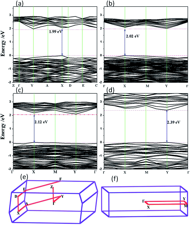 |
| | Fig. 4 Calculated band structures of rP using the HSE06 functional: (a) bulk, (b) trilayer, (c) bilayer, (d) monolayer. (e) and (f) are the associated Brillouin zone of rP in the bulk and 2D configurations, respectively. | |
According to the total DOS of the rP bulk and 2D systems in Fig. 5, the hybrid sp3 bonding states of the P atoms are mainly located at the lower energy region of the valence band (VB) and the higher energy region of the conduction band (CB), while the VBM and CBM are mainly predominated by P 2p states. In general, no great changes can be seen in Fig. 5, except for the broadened conduction band structure of the rP monolayer. Thus, in the following sections, we focus our attention on rP in the bulk and monolayer systems. For further information about the electronic states of rP in the bulk and monolayer systems, we investigated the projected DOS of different atoms on the tubes. The VBM of bulk rP is mostly contributed to by P 2p states from the atom numbered 18, and the CBM is predominated by P 2p states of all atoms and some 2s states of the atom numbered 9 (see the ESI, Fig. S1†). For monolayer rP, the 2p states of the P atom numbered 9 make a major contribution to the VBM compared to those of the atom numbered 18 (see the ESI, Fig. S2†), and no significant differences were found between the conduction bands of different atoms.
 |
| | Fig. 5 Total and partial density of states for rP using the HSE06 functional: (a) bulk, (b) trilayer, (c) bilayer, (d) monolayer. | |
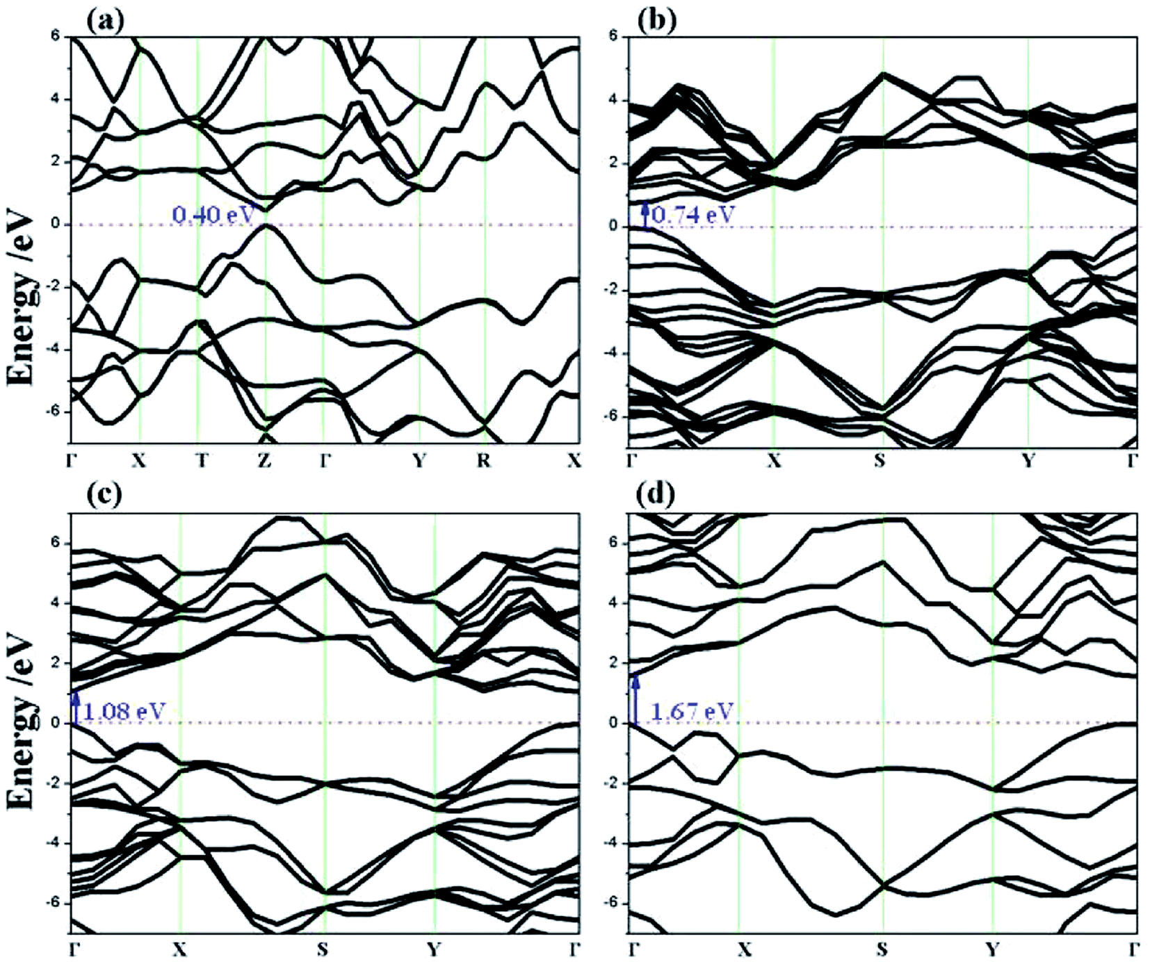
3.2.2 The band structure of bP. In the case of bP, an apparent significant difference compared to the rP system is the direct band gap of bP in both the bulk and monolayer forms (Fig. 6). In the bulk system, the CBM and the VBM are located at the Z point, and in the 1–3 layer systems they shift to the Г point, where the band splits into more levels with the addition of extra layers. The band gaps of the few-layer bP systems show a strong layer-dependent evolution, increasing from 0.40 eV in the bulk form, to 0.74 eV in the trilayer system, to 1.08 eV in the bilayer system, and eventually to 1.67 eV in the monolayer system. This agrees well with Qiao's22 results, which show a change from 0.75 to 1.51 eV going from the trilayer to monolayer systems, and is also consistent with the experimentally measured value of 0.31–0.36 eV for bulk bP (ref. 44–46) and 1.45 eV for monolayer bP.21
 |
| | Fig. 6 Calculated band structures of bP using the HSE06 functional: (a) bulk, (b) trilayer, (c) bilayer, (d) monolayer. | |
Further analysis on the geometry-dependent band gap shows that it is modulated by the interlayer spacing (Fig. 7). The band gap firstly increases monotonically with increasing distance between the two layers, and then tends to remain steady beyond 10 Å, at a value close to that of the monolayer system (1.67 eV). Using the GW approximation, Rudenko47 revealed an important role of the interlayer distance in modifying the band gap. He believed that by introducing the repulsive hopping parameter (t⊥) between structures with more layers, the band gap could be qualitatively reduced. According to the projected DOS for bP in Fig. 8, we note that all essential features remain the same as those in bulk bP, with the exception of the conduction band span, which widens from 5 eV to 8 eV from the 3-layer system to the 1-layer system. It is clear that the covalent bond in bP is mainly contributed to by the p–p bonding states at the valence band top and conduction band bottom, and most s–p bonding states are located at the lower energy region of the VB and higher energy level of the CB. Interestingly, the change of standard Gibbs free energy (ΔG) in the water-splitting reaction is 1.23 eV.48 Therefore, the band gap of a visible-light-driven photocatalyst for H2 evolution from water needs to be in the range of 1.2–3.0 eV. The above discussions suggest that monolayer bP has the potential to be a novel material for photocatalysis.
 |
| | Fig. 7 The band gap of the bilayer system as a function of the interlayer spacing (distance/Å). | |
 |
| | Fig. 8 Total and partial density of states for bP using the HSE06 functional: (a) bulk, (b) trilayer, (c) bilayer, (d) monolayer. | |
3.3 Effective mass of photogenerated electrons and holes
Changes in effective mass can influence charge carrier transport properties. If there is no change in the time scale for quasiparticle scattering, then the mobility of charge carriers is inversely proportional to their effective mass. To shed light on the mobility rate of the electron–hole pairs, the relative effective mass of the electron and hole in the rP and few-layer bP systems were computed using the following formula:49,50| |
 | (1) |
where m* is the effective mass of the charge carriers in the unit of free-electron mass (me) and a is the coefficient of the second-order term in a quadratic fit of E(k) curves for the band edge corresponding to the wave vector k. It is well known that the smaller the effective mass, the higher the mobility of the charge carrier. Furthermore, a large difference in the effective mass of the electrons  and that of the holes
  implies a greater difference in electron–hole mobility.39 Thus the relative ratio of the effective masses of the electrons and holes may determine the recombination rate of the photointroduced carriers. Here, we give the ratio value of
  and
and  as follows:
| |
 | (2) |
Table 2 lists  ,
,  and the ratio value D of the rP and bP systems along the Г–X, Г–Y and Z–Г directions in the first Brillouin zone of the bulk systems, and Г–X and Г–Y for the monolayer rP and few-layer bP systems. The
  values along Г–X and Г–Y for rP in the bulk form are 0.984 and 0.461, respectively, which are lower than that of TiO2 (about 1 me),48 indicating that the electrons in the CB can transfer more rapidly to the surface. Meanwhile, along the Z–Г direction, the
  value (6.727) is 14 times higher than that along Г–Y and 6 times higher than that along the Г–X direction. In the monoclinic rP crystalline cell of P2/c space group, the extending directions of Г–X, Г–Y and Z–Г are the same directions as the crystallographic axes of a, b, and c. Therefore, the electronic mobility is slowest along the c axis, i.e. along the direction of composite laminated structure, the electronic mobility is blocked. Unlike the case of
  , the values of
  along different directions show minor differences, and our results are 0.778 for the a axis direction, and 1.502 and 2.199 for the b and c axis directions, respectively. The
  ratio of 0.307 along Г–Y is much smaller than 1, indicating the greater difference between the photogenerated hole and electron mobility. From the bulk to the monolayer systems,
  (0.473 for the monolayer) along the Г–X direction is twofold less, while the value of
  is slightly increased to 1.069, producing a considerably reduced ratio of 0.409, leading to a suppressed recombination efficiency. Both
  and
and  along Г–Y exhibit small changes, and the ratio remains a relatively small value. Thus, varying the dimensions of rP is conducive to improving the mobility and separation efficiency and thus facilitating photocatalysis.
Table 2 The effective mass of electrons  and holes
  in the unit of free-electron mass for rP and bP in the bulk and few-layer systems along different directions in reciprocal space
| |
System |
Г–X |
Г–Y |
Z–Г |
| rP in bulk form. rP in monolayer form. bP in bulk form. bP in trilayer form. bP in bilayer form. bP in monolayer form. |
 |
rP-Bulka |
0.984 |
0.461 |
6.727 |
| rP-MonoLb |
0.437 |
0.544 |
— |
| bP-Bulkc |
0.138 |
1.203 |
0.171 |
| bP-ThiLd |
0.194 |
1.138 |
— |
| bP-BiLe |
0.202 |
1.207 |
— |
| bP-MonoLf |
0.188 |
1.119 |
— |
 |
rP-Bulk |
0.778 |
1.502 |
2.199 |
| rP-MonoL |
1.069 |
1.863 |
— |
| bP-Bulk |
0.124 |
0.630 |
0.412 |
| bP-ThiL |
0.170 |
1.543 |
— |
| bP-BiL |
0.164 |
1.923 |
— |
| bP-MonoL |
0.162 |
8.316 |
— |
| D |
rP-Bulk |
1.265 |
0.307 |
3.059 |
| rP-MonoL |
0.409 |
0.290 |
— |
| bP-Bulk |
1.113 |
1.909 |
0.415 |
| bP-ThiL |
1.141 |
0.738 |
— |
| bP-BiL |
1.232 |
0.628 |
— |
| bP-MonoL |
1.160 |
0.135 |
— |
Using the same aforementioned method, the mobility of bP was examined. As seen in Table 2, the values for  along Г–X and Z–Г are 0.138 and 0.171, respectively, while the electrons have a large effective mass of 1.203 along Г–Y, which is about 9 times that along Г–X. Additionally, the holes in bulk bP are lighter than electrons; the values of
  are 0.124, 0.412 and 0.630 in the Г–X, Z–Г and Г–Y directions, respectively. These calculated results are in good agreement with Morita's experimental values.43 When bulk bP is cut down to a few layers, the effective mass for the electrons of bP does not show a significant quantitative change. The value of
  along Г–X is 0.194 for the trilayer system, 0.202 for the bilayer system, and 0.188 for the monolayer system with differences of 0.038–0.046 compared to the bulk bP value. From the monolayer to the trilayer systems, the change in
  along Г–Y is not significant compared with that of bulk bP. However,
  along Г–Y is increased with the reduced number of layers, varying from 1.543 in the trilayer system, 1.923 in the bilayer system, and 8.316 in the monolayer system. Furthermore, the ratio D is affected by the number of layers. In the monolayer system, D along Г–Y is 0.135, which is obviously smaller than that in the bulk, two- and three-layer systems. So we consider the layer-control modulation of bP to be a modification strategy for good mobility and potential electron and hole separation, which is beneficial for better photocatalytic performance.
In a photocatalytic process, the net quantum efficiency is a function of photo-excitation, bulk diffusion and surface consumption. Additionally, the internal electric field is predominantly responsible for the diffusion process of charge carrier separation and transfer orientation.51 Considering that the anisotropy of the structure induces the presence of an internal electrostatic field, the diffusion process of the carriers will be significantly affected. Therefore, the electrostatic potentials of rP and bP both in the bulk and in few-layer forms were calculated. The average electrostatic potential of the unit cell of the bulk rP along the crystallographic axes directions is shown in Fig. 9. It is obvious that the periodic potential trough in the direction of the Z axis is much greater than that of the X and Y axes. Ultimately, electrons would be unable to cross the electrostatic potential barrier along the Z axis and would prefer to transfer within the [100] and [010] facets. As for monolayer rP, the periodic potential trough along the X and Y axes is much smaller than that in bulk rP. Thus, the constraint of the charge carrier mobility in the plane of monolayer rP is much smaller than that in bulk rP. From the above, the configuration of monolayer rP not only profits by reducing the effective mass of the charges but also benefits by lowering the electrostatic resistance.
 |
| | Fig. 9 Electrostatic potential of rP: (a1), (a2) and (b) in the direction of [100], [010], [001] of the bulk form, respectively; (c1) and (c2) in the direction of [100] and [010] of the monolayer system, respectively. | |
Fig. 10 illustrates the average electrostatic potential of bP in the bulk and few-layer forms. Having different curvature, the line-graphs in Fig. 10a1, a2 and e indicate that the periodic potential trough in the direction of the Y axis is much greater than that of the X and Z axes, i.e. the obstacle to electron migration within the [010] facets is larger than that within the [100] and [001] facets. This may be one of the reasons behind the previous results52,53 where it was found that the charge carrier mobility along the Y direction is faster than that along the X and Z directions in bulk bP. Taking the different effective mass of the charges along the different directions into account, we believe that the transfer of charge carriers from one layer to the neighboring one is inconvenient. In the few-layer systems, the periodic potential trough is gradually decreased from the trilayer to monolayer systems (Fig. 10), which is in agreement with the previous study54 where the anisotropy of mobility between the X and Y directions in thin film bP is smaller than that in bulk bP. Similar to rP, the monolayer configuration is beneficial in promoting charge transfer in the bP system.
 |
| | Fig. 10 Electrostatic potential of bP: (a1, b1, c1, d1) in the [100] direction of the bulk, trilayer, bilayer, and monolayer systems, respectively; (a2, b2, c2, d2) in the [010] direction of the bulk, trilayer, bilayer, and monolayer systems, respectively; (e) in the [001] direction of the bulk system. | |
3.4 The energy positions of the conduction and valence bands
The transfer of electrons between the semiconductor and adsorbed reactants is the crucial step in photocatalytic reactions. The difference in energy between the top of the valence band (EVB) and the bottom of the conduction band (ECB) is the fundamental property of a semiconductor photocatalyst that dictates whether an electron transfer between the semiconductor and sorbate is feasible. Here the EVB and ECB of the rP and bP systems are estimated from the electronegativity of the P atom and the respective band gap using semi-empirical relations (3) and (4):55| |
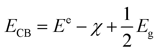
 | (3) |
where Ee is the energy of free electrons at the hydrogen scale (Ee = −4.5 eV), χ is the electronegativity of the semiconductor (for P, χ = 5.62),56 and Eg is the band gap of the semiconductor.
All the results of EVB and ECB are presented in Fig. 11. The ECB of bulk rP (−0.22 eV) indicates that rP is strong enough to photocatalyze H2 evolution from water, and its EVB is 0.65 eV below the energy level of E(O2/H2O). Thus, bulk rP can theoretically be employed as a photocatalyst for splitting water into H2 and O2. In monolayer rP, the energy levels shift to a lower energy region, and the conduction band edge drops down to −0.01 eV. Therefore, the reduction power has been weakened, while the oxidization potential is greatly enhanced due to its EVB value shifting down by 0.61 eV. For the bP systems, the band edge energies of the CB and VB are constantly moving with the changing band gap energies. The ECB varies from −0.92 eV in the bulk system to −0.75, −0.58 and −0.33 eV in trilayer, bilayer and monolayer bP, respectively. Meanwhile, the EVB drops to lower positions gradually with more and more positive values, indicating that the oxidation capacity is increased gradually from the bulk to monolayer systems. Finally, the computed EVB (1.34 eV) and ECB (−0.33 eV) of monolayer bP are 0.11 eV below the water oxidation potential and 0.33 eV above the water reduction potential, respectively. From these analyses, we can find that rP has better oxidation ability, while it has poorer reduction ability than bP.
 |
| | Fig. 11 Position of the conduction band edge (ECB) and the valence band edge (EVB) of the rP and bP systems with respect to normal hydrogen electrode (NHE) scale. The solution effect has not been examined in the band edge calculations. | |
3.5 Optical absorption spectra
The study of the optical properties of a photocatalyst is significant from an application point of view. The absorption coefficient indicates the fraction of energy loss of the electromagnetic wave when it passes through a unit thickness of the material. We obtain the spectra of rP and bP using the Fermi golden rule within the dipole approximation from the HSE06 wave functions. The absorption coefficient η(ω) can be obtained based on the following formula:57| |
 | (5) |
where ε1 and ε2 are the real and imaginary parts of the dielectric tensor, respectively. The real part of the dielectric tensor ε1 is obtained by a Kramers–Kronig transformation. Furthermore, the imaginary part of the dielectric function is given by the following expression:58| |
 | (6) |
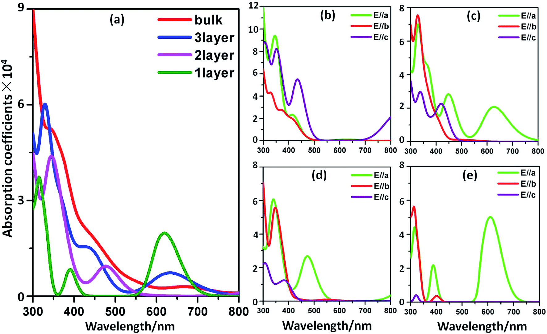
where Ω, ω, u, ν, and c are the unit-cell volume, photon frequencies, the vector defining the polarization of the incident electric field, valence bands, and conduction bands, respectively. The calculated optical spectra of rP as a function of light wavelength are shown in Fig. 12. From Fig. 12a, the absorption spectra of bulk rP using “polycrystalline” polarization (optical absorption is averaged over all polarization directions) show substantial adsorption in the visible light range and the largest wavelength is close to 550 nm. It is noted that the optical absorption curves along the three polarization directions are different from each other, demonstrating the optical anisotropy of the material. As the bulk form is cut into the monolayer form, the optical absorption coefficient in the E//a and E//b polarization directions becomes larger than that along the E//c polarization direction (Fig. 12b), which may arise from the decrease in atom numbers along c axis. Therefore, in monolayer rP, most of the absorption is contributed to by the absorption along the E//a and E//b directions. Although the absorption threshold shows a blue-shift of about 50 nm to 500 nm, the rP nanosheet still retains a strong response in the visible-light range.
 |
| | Fig. 12 Absorption coefficient spectra of rP: (a) for direction-averaged and light incident polarized along the E//a, E//b and E//c directions in the bulk form; (b) for the monolayer system. We employ a 0.1 eV smearing in these plots. | |
The optical spectra of the bP systems are illustrated in Fig. 13, where the average absorption curves over all polarization directions in Fig. 13a are different from the bulk to few-layer forms. It is clear that the few-layer nanosheets show notable adsorption in the visible light range, especially for the monolayer system. There is a conspicuous absorption peak approximately located at 620 nm. Furthermore, the spectra in Fig. 13b–e show the optical properties at different polarization directions in the bulk, trilayer, bilayer and monolayer systems, respectively. It's clear that the absorption properties of bP in the bulk and 2D nanosheet forms are both anisotropic. Clearly, the absorption spectrum along the E//c direction shows a decline as the number of layers is reduced, while in the monolayer, the visible-light absorption is mainly due to the light incident along E//a. In Qiao's work,22 linear dichroism in few-layer black phosphorus between the perpendicular in-plane directions was also found in the light absorption spectra, which unanimously indicated the anisotropic optical properties of the bP few-layer systems. From those analyses, we believe that rP and bP can be excited via visible light when used as photocatalyst.
 |
| | Fig. 13 Absorption spectra of bP: (a) for direction-averaged; (b, c, d, e) for light incident polarized along the (100), (010) and (001) directions in the bulk, trilayer, bilayer, and monolayer systems, respectively. We employ a 0.1 eV smearing in these plots. | |
4. Conclusion
In summary, we have systematically studied the electronic structures and potential photocatalytic properties of red and black phosphorous in bulk and few-layer forms. As an indirect band gap semiconductor, bulk rP presents an ideal band gap (1.99 eV) as well as very strong optical absorption abilities to absorb the maximum portion of solar visible light. Additionally, rP exhibits appropriate conduction-band minimum and valence-band maximum potentials, which is desirable in photocatalyzing H2 and O2 generation from water. This oxidation ability is better than that observed in the bP systems. We have found that rP transforms from an indirect band gap semiconductor into a direct one, passing from the bulk form to monolayer nanosheet form, induced by perpendicular quantum confinement, and the higher mobility of charge carriers favors the photocatalysis. As for the bP systems, the band gap is layer-dependent, increasing to 1.67 eV in the monolayer system from 0.40 eV in the bulk form. Furthermore, the band gap is sensitive to the widening interlayer spacing, and is close to the value of the monolayer if the distance reaches 10 Å. The separation rate of the charge carriers is improved due to the absent electrostatic potential trough within the monolayer facet. The opened band gap of the monolayer system puts the band edge at an optimal position, which offers bP potential applications as a photocatalyst.
Acknowledgements
This research was supported by the National Natural Science Foundation of China (21171039 and 21373048), Natural Science Foundation of Fujian Province (2016J01687) and the Fund of Key Laboratory of Optoelectronic Materials Chemistry and Physics, Chinese Academy of Sciences (2008DP173016).
References
- Z. H. Kang, C. H. A. Tsang, N. B. Wong, Z. D. Zhang and S. T. Lee, J. Am. Chem. Soc., 2007, 129, 12090–12091 CrossRef CAS PubMed.
- Z. H. Kang, Y. Liu, C. H. A. Tsang, D. D. D. Ma, X. Fan, N. B. Wong and S. T. Lee, Adv. Mater., 2009, 21, 661–664 CrossRef CAS.
- Y. D. Chiou and Y. J. Hsu, Appl. Catal., B, 2011, 105, 211–219 CrossRef CAS.
- F. Wang, W. K. H. Ng, J. C. Yu, H. J. Zhu, C. H. Li, L. Zhang, Z. F. Liu and Q. Li, Appl. Catal., B, 2012, 111–112, 409–414 CrossRef CAS.
- G. Liu, P. Niu, L. Yin and H. M. Cheng, J. Am. Chem. Soc., 2012, 134, 9070–9073 CrossRef CAS PubMed.
- C. Z. Yan, C. M. Raghavan and D. J. Kang, Mater. Lett., 2014, 116, 341–344 CrossRef CAS.
- G. Liu, L. C. Yin, P. Niu, W. Jiao and H. M. Cheng, Angew. Chem., Int. Ed., 2013, 52, 6242–6245 CrossRef CAS PubMed.
- U. Braun and B. Schartel, Macromol. Chem. Phys., 2004, 205, 2185–2196 CrossRef CAS.
- M. Scheer, G. B. Balázs and A. Seitz, Chem. Rev., 2010, 110, 4236–4256 CrossRef CAS PubMed.
- E. C. Koch, Propellants, Explos., Pyrotech., 2008, 33, 165–176 CrossRef CAS.
- N. R. Panyala, E. M. Pena-Mendez and J. Havel, Rapid Commun. Mass Spectrom., 2012, 26, 1100–1108 CrossRef CAS PubMed.
- G. Liu, P. Niu and H. M. Cheng, ChemPhysChem, 2013, 14, 885–892 CrossRef CAS PubMed.
- H. F. Dang, X. F. Dong, Y. C. Dong, H. B. Fan and Y. F. Qiu, RSC Adv., 2014, 4, 44823–44826 RSC.
- Y. P. Yuan, S. W. Cao, Y. S. Liao, L. S. Yin and C. Xue, Appl. Catal., B, 2013, 140, 164–168 CrossRef.
- Z. Shi, X. Dong and H. Dang, Int. J. Hydrogen Energy, 2016, 41, 5908–5915 CrossRef CAS.
- N. Goodman, L. Ley and D. Bullett, Phys. Rev. B: Condens. Matter Mater. Phys., 1983, 27, 7440–7450 CrossRef CAS.
- H. Asahina and A. Morita, J. Phys. C: Solid State Phys., 1984, 17, 1839–1852 CrossRef CAS.
- G. Seifert and E. Hernandez, Chem. Phys. Lett., 2000, 318, 355–360 CrossRef CAS.
- I. Cabria and J. W. Mintmire, Europhys. Lett., 2004, 65, 82 CrossRef CAS.
- L. K. Li, Y. J. Yu, G. J. Ye, Q. Q. Ge, X. D. Ou, H. Wu, D. L. Feng, X. H. Chen and Y. B. Zhang, Nat. Nanotechnol., 2014, 9, 372–377 CrossRef CAS PubMed.
- L. Han, A. T. Neal, Z. Zhu, Z. Luo, X. F. Xu, D. Tománek and P. D. Ye, ACS Nano, 2014, 8, 4033–4041 CrossRef PubMed.
- J. Qiao, X. Kong, Z. X. Hu, F. Yang and W. Ji, Nat. Commun., 2014, 5, 4475 CAS.
- X. Han, H. M. Stewart, S. A. Shevlin, C. R. Catlow and Z. X. Guo, Nano Lett., 2014, 14, 4607–4614 CrossRef CAS PubMed.
- D. Çakır, C. Sevik and F. M. Peeters, Phys. Rev. B: Condens. Matter Mater. Phys., 2015, 92, 165406 CrossRef.
- K. Dolui and S. Y. Quek, Sci. Rep., 2015, 5, 11699 CrossRef PubMed.
- Y. X. Deng, Z. Luo, N. J. Conrad, H. Liu, Y. Gong, S. Najmaei, P. M. Ajayan, J. Lou, X. Xu and P. D. Ye, ACS Nano, 2014, 8, 8292–8299 CrossRef CAS PubMed.
- L. Kou, T. Frauenheim and C. Chen, J. Phys. Chem. Lett., 2014, 5, 2675–2681 CrossRef CAS PubMed.
- J. Dai and X. C. Zeng, J. Phys. Chem. Lett., 2014, 5, 1289–1293 CrossRef CAS PubMed.
- M. Engel, M. Steiner and P. Avouris, Nano Lett., 2014, 14, 6414–64617 CrossRef CAS PubMed.
- K. J. Koski and Y. Cui, ACS Nano, 2013, 7, 3739–3743 CrossRef CAS PubMed.
- W. Xin Chen, M. C. Johan, D. Kazunari and A. Markus, Nat. Mater., 2009, 8, 76–80 CrossRef PubMed.
- R. Lu, F. Li, J. Salafranca, E. Kan, C. Xiao and K. Deng, Phys. Chem. Chem. Phys., 2014, 16, 4299–4304 RSC.
- M. A. Bizeto, A. L. Shiguihara and V. R. L. Constantino, J. Mater. Chem., 2009, 19, 2512 RSC.
- S. J. Clark, M. D. Segall, C. J. Pickard, P. J. Hasnip, M. I. J. Probert, K. Refson and M. C. Payne, Z. Kristallogr., 2005, 220, 567–570 CAS.
- J. P. Perdew, Phys. Rev. B: Condens. Matter Mater. Phys., 1981, 23, 5048–5079 CrossRef CAS.
- J. P. Perdew, J. A. Chevary, S. H. Vosko, K. A. Jackson, M. R. Pederson, D. J. Singh and C. Fiolhais, Phys. Rev. B: Condens. Matter Mater. Phys., 1992, 46, 6671–6687 CrossRef CAS.
- S. Grimme, J. Comput. Chem., 2006, 27, 1787–1799 CrossRef CAS PubMed.
- J. Heyd and G. E. Scuseria, J. Chem. Phys., 2004, 120, 7274–7280 CrossRef CAS PubMed.
- V. H. Thurn and H. Krebs, Acta Crystallogr., 1969, B25, 125–135 CrossRef.
- M. Ruck, D. Hoppe, B. Wahl, P. Simon, Y. Wang and G. Seifert, Angew. Chem., Int. Ed., 2005, 44, 7616–7619 CrossRef CAS PubMed.
- S. Bocker and M. Haser, Z. Anorg. Allg. Chem., 1995, 621, 258–286 CrossRef.
- R. Hultgren, N. S. Gingrich and B. E. Warren, J. Chem. Phys., 1935, 3, 351 CrossRef CAS.
- A. Morita, Appl. Phys. A, 1986, 39, 227–242 CrossRef.
- D. Warschauer, J. Appl. Phys., 1963, 34, 1853 CrossRef CAS.
- Y. Maruyama, S. Suzuki, K. Kobayashi and S. Tanuma, Physica B+C, 1981, 105, 99–102 CrossRef CAS.
- S. Narita, Y. Akahama, Y. Tsukiyama, K. Muro, S. Mori, S. Endo, M. Taniguchi, M. Seki, S. Suga and A. Mikuni, Physica B+C, 1983, 117, 422–424 CrossRef.
- A. N. Rudenko and M. I. Katsnelson, Phys. Rev. B: Condens. Matter Mater. Phys., 2014, 89, 201408 CrossRef.
- T. Sakata and E. Pelizzetti, Photocatalysis: Fundamentals and Applications, Wiley, New York, 1989 Search PubMed.
- M. Ali Omar, Elementary solid state physics, Addi son-Wesley Pubf ishing Gompony, 1975 Search PubMed.
- L. Thulin and J. Guerra, Phys. Rev. B: Condens. Matter Mater. Phys., 2008, 77, 1951121–1951125 CrossRef.
- B. O'Regan, J. Moser, M. Anderson and M. Graetzel, J. Phys. Chem., 1990, 94, 8720–8726 CrossRef.
- A. Morita, Appl. Phys. A: Solids Surf., 1986, 39, 227–242 CrossRef.
- H. Asahina, K. Shindo and A. Morita, J. Phys. Soc. Jpn., 1982, 51, 1193–1199 CrossRef CAS.
- F. Xia, H. Wang and Y. Jia, arXiv preprint arXiv:1402.0270, 2014.
- Y. I. Kim, S. J. Atherton, E. S. Brigham and T. E. Mallouk, J. Phys. Chem., 1993, 97, 11802–11810 CrossRef CAS.
- R. G. Pearson, Inorg. Chem., 1988, 27, 734–740 CrossRef CAS.
- A. Read and R. Needs, Phys. Rev. B: Condens. Matter Mater. Phys., 1991, 44, 13071–13073 CrossRef.
- S. Saha, T. P. Sinha and A. Mookerjee, Phys. Rev. B, 2000, 62, 8828 CrossRef CAS.
Footnote |
| † Electronic supplementary information (ESI) available. See DOI: 10.1039/c6ra10907a |
|
| This journal is © The Royal Society of Chemistry 2016 |
Click here to see how this site uses Cookies. View our privacy policy here. 
 ratio are effectively modulated by strain. Çakır et al.24 systematically investigated the influence of different stacking types on the electronic and optical properties of bP and found that the band gap and optical response of bilayer and trilayer bP are very sensitive to the number of layers and the stacking type. Additionally, Dolui et al.25 found that when a black phosphorus film is sufficiently thin, a Dirac cone could be induced in the system when increasing the external vertical electric field beyond the critical field, and the electric field strength can tune the position of the Dirac cone and the Dirac–Fermi velocities. Due to its particular photoelectronic characteristics, monolayer bP is an appealing material that can be incorporated into various electronic devices and photovoltaic devices including p–n junctions,26 gas sensors,27 solar cells28 and photodetectors.29 Although many unique features of bP have been reported recently, many of its special properties have not yet been discovered.
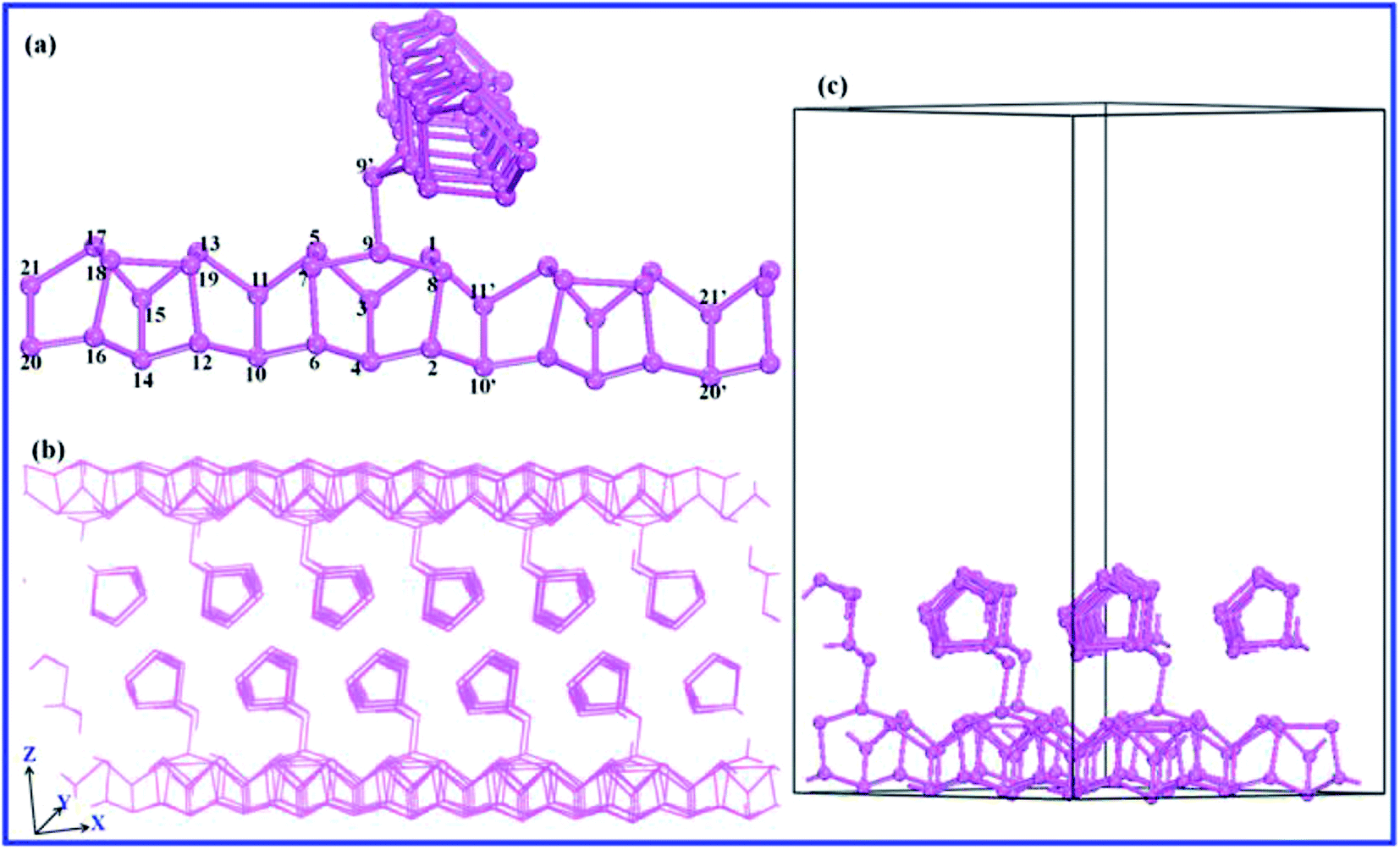


 and that of the holes
  implies a greater difference in electron–hole mobility.39 Thus the relative ratio of the effective masses of the electrons and holes may determine the recombination rate of the photointroduced carriers. Here, we give the ratio value of
  and
and  as follows:
 ,
,  and the ratio value D of the rP and bP systems along the Г–X, Г–Y and Z–Г directions in the first Brillouin zone of the bulk systems, and Г–X and Г–Y for the monolayer rP and few-layer bP systems. The
  values along Г–X and Г–Y for rP in the bulk form are 0.984 and 0.461, respectively, which are lower than that of TiO2 (about 1 me),48 indicating that the electrons in the CB can transfer more rapidly to the surface. Meanwhile, along the Z–Г direction, the
  value (6.727) is 14 times higher than that along Г–Y and 6 times higher than that along the Г–X direction. In the monoclinic rP crystalline cell of P2/c space group, the extending directions of Г–X, Г–Y and Z–Г are the same directions as the crystallographic axes of a, b, and c. Therefore, the electronic mobility is slowest along the c axis, i.e. along the direction of composite laminated structure, the electronic mobility is blocked. Unlike the case of
  , the values of
  along different directions show minor differences, and our results are 0.778 for the a axis direction, and 1.502 and 2.199 for the b and c axis directions, respectively. The
  ratio of 0.307 along Г–Y is much smaller than 1, indicating the greater difference between the photogenerated hole and electron mobility. From the bulk to the monolayer systems,
  (0.473 for the monolayer) along the Г–X direction is twofold less, while the value of
  is slightly increased to 1.069, producing a considerably reduced ratio of 0.409, leading to a suppressed recombination efficiency. Both
  and
and  along Г–Y exhibit small changes, and the ratio remains a relatively small value. Thus, varying the dimensions of rP is conducive to improving the mobility and separation efficiency and thus facilitating photocatalysis.
 and holes
  in the unit of free-electron mass for rP and bP in the bulk and few-layer systems along different directions in reciprocal space


 along Г–X and Z–Г are 0.138 and 0.171, respectively, while the electrons have a large effective mass of 1.203 along Г–Y, which is about 9 times that along Г–X. Additionally, the holes in bulk bP are lighter than electrons; the values of
  are 0.124, 0.412 and 0.630 in the Г–X, Z–Г and Г–Y directions, respectively. These calculated results are in good agreement with Morita's experimental values.43 When bulk bP is cut down to a few layers, the effective mass for the electrons of bP does not show a significant quantitative change. The value of
  along Г–X is 0.194 for the trilayer system, 0.202 for the bilayer system, and 0.188 for the monolayer system with differences of 0.038–0.046 compared to the bulk bP value. From the monolayer to the trilayer systems, the change in
  along Г–Y is not significant compared with that of bulk bP. However,
  along Г–Y is increased with the reduced number of layers, varying from 1.543 in the trilayer system, 1.923 in the bilayer system, and 8.316 in the monolayer system. Furthermore, the ratio D is affected by the number of layers. In the monolayer system, D along Г–Y is 0.135, which is obviously smaller than that in the bulk, two- and three-layer systems. So we consider the layer-control modulation of bP to be a modification strategy for good mobility and potential electron and hole separation, which is beneficial for better photocatalytic performance.