
CdO nanoflake arrays on ZnO nanorod arrays for efficient detection of diethyl ether†
Sheng-Guang Ban,
Xiao-Hua Liu,
Tao Ling,
Cun-Ku Dong,
Jing Yang and
Xi-Wen Du*
Key Laboratory of Advanced Ceramics and Machining Technology, Ministry of Education (Tianjin University), Institute of New-Energy Materials, School of Materials Science and Engineering, Tianjin University, Tianjin 300072, People's Republic of China. E-mail: xwdu@tju.edu.cn
First published on 22nd December 2015
Abstract
We report the template synthesis and gas detection of CdO porous nanoflake arrays (P-NFAs) on ZnO nanorod arrays. The P-NFAs possesses a large surface-to-volume ratio, high-energy exposed surface, unimpeded channels for gas flow, and hierarchical holes. As a result, the device exhibits excellent sensing properties upon exposure to diethyl ether.
Highly sensitive gas sensors play a crucial role in air monitoring, industrial safety, health, etc.1 It was demonstrated that well-designed nanostructures can improve the performance of gas sensors remarkably.2 Recently, two-dimensional (2D) nanostructures received considerable attention for gas sensing applications due to their unique advantages such as large surface-to-volume ratio, high-energy exposed surface, and easy depletion of carriers.3 Hitherto, several categories of materials, e.g. graphene,4 transition-metal chalcogenides (MoS2,5 MoO3,6 MoSe2,7 WS2,8 WO3 (ref. 9)), and traditional semiconductor oxides (ZnO10 and SnO2 ref. 2b and 11), have been adopted to construct nanoflakes and utilized for gas sensors. The common preparation of nanoflake-based gas sensors involves the synthesis of free standing nanoflakes and then coating them on an insulating substrate.9,10a However, this process usually causes serious stacking of nanoflakes. Resultantly, a large portion of the surfaces of nanoflakes became inaccessible, deteriorating the final performance.3b To overcome this problem, nanoflake arrays (NFAs) were grown in situ on the substrates between the working electrodes.12 However, the in situ synthesis always produces a continuous seed layer at the bottom of NFAs, which serves as a channel for direct short of electrical current, thus screens the effect of NFAs.12
Diethyl ether (DEE), known as an inflammable and explosive gas, is an important chemical for industrial production. Meanwhile, it is harmful to human health and causes examination in case of excessive inhalation. So far, several works reported the detection of DEE with CdO nanostructures.13 For instance, Fu et al. employed a leaf-like CdO material to realize fast response to DEE, however, the low selectivity makes it difficult to distinguish DEE from the other volatile organic compounds.13a Very recently, three-dimensional hierarchical CdO nanostructure was fabricated to detect DEE on the basis of a cataluminescence (CTL) effect.13b,13c As compared with traditional gas sensors, the CTL-based device is complicated due to the utilization of optical system for collection and analysis of luminescent signals. Thus it is still a big challenge to develop a cheap and effective device for the detection of DEE.
In previous works, we exploited a thermal decomposition route to grow Cd NFAs on various substrates.14 Herein, we transform the Cd NFAs into CdO NFAs conveniently by the oxidization in air. Particularly, we design a double layer (DL) structure with CdO nanoflake arrays (NFAs) on ZnO nanorods arrays (NRAs) for DEE detection (Scheme 1). First, Cd NFAs were grown on the top of ZnO NRAs, and then the Cd NFAs were oxidized in air to obtain different CdO nanostructures. ZnO NRAs play dual roles in improving the final performance. On one hand, they serve as a discontinuous substrate to separate the seed layer but keep NFAs continuous. On the other hand, their electrical resistance is much higher than that of CdO NFAs,15 ensuring that the electrical current flows only through CdO NFAs. In this way, we eliminate the influence of seed layer and realize the gas detection with pure CdO NFAs. Moreover, we found that the morphology of CdO products can be tuned by adjusting the oxidization temperature, that is, normal NFAs (N-NFAs), porous NFAs (P-NFAs) and sponge-like structure (S-structure) can be obtained at 360, 400, and 440 °C, respectively. The DL devices based on the above structures were examined simultaneously in the same apparatus, so as to assess the influence of morphology. Among them, P-NFAs achieved the best gas sensing properties, including the highest sensitivity, the fastest response and recovery, and the highest selectivity, indicating that appropriate nanostructures are helpful on enhancing gas sensing performance.
 | ||
| Scheme 1 Schematic illustration on the preparation of DL device with CdO nanostructures on ZnO NRAs. | ||
Fig. 1a displays scanning electron microscopy (SEM) images of as-grown ZnO NRAs from side view. The ZnO nanorods uniformly distribute on the glass substrate, and exhibit a regular hexagonal shape with diameters of 300–500 nm, lengths of 2 μm, and spacings of 100–200 nm. The X-ray diffraction (XRD) pattern of ZnO NRAs in Fig. 1d presents solely an intensive peak corresponding to ZnO (0002) plane, suggesting the single-crystal structure and aligned orientation of ZnO nanorods. The as-prepared Cd nanoflakes with size ranging from 1 to 3 μm orderly arrange to form NFAs on substrate (Fig. S1a†). High resolution transmission electron microscope (HRTEM) image and selected area electron (SAED) pattern illustrate a single crystal structure with exposed (002) surface (Fig. S1b†). After being oxidized at 360 °C, Cd NFAs were transformed into CdO N-NFAs, and their morphology was retained successfully (Fig. 1b and d). The NFAs are propitious to the injection of target gas. Meanwhile, numerous contacts among CdO nanoflakes favor gas sensitivity according to grain boundary contact theory.16 Nevertheless, underneath the NFAs emerges a continuous CdO layer, which can cause short circuit of CdO N-NFAs (Fig. 1b). To address this issue, Cd NFAs were grown on the top of ZnO NRAs. As seen in Fig. 1c and S2,† after the oxidization at 360 °C, the continuous CdO layer cannot be observed any more, and the CdO N-NFAs directly contact with ZnO NRAs to form a double layer structure which is designated as DL 360 (the number denotes the oxidization temperature). Meanwhile, the morphology of the CdO N-NFAs on ZnO NRAs is same as that grown on glass substrates (Fig. 1c), and so does their phase structure (Fig. 1d).
 | ||
| Fig. 1 Characterizations of the ZnO NRAs, CdO N-NFAs, and DL structure. (a–c) are side-view SEM images of ZnO NRAs, CdO N-NFAs, and DL360, respectively, on glass substrate. The insets are corresponding top-view SEM images. (d) XRD patterns of ZnO NRs, CdO N-NFAs, and DL360. (e) The initial resistance of ZnO NRs, CdO N-NFAs and DL360 in air at 215 °C, the inset is the structure of DL360 gas sensor. (f) Gas response of ZnO NRAs, CdO N-NFAs and DL360 to 100 ppm DEE at 215 °C. | ||
We then assembled three devices with ZnO NRAs, CdO N-NFAs, and DL 360, respectively, to measure their electrical resistance (see the inset of Fig. 1e). As depicted in Fig. 1e, ZnO NRAs own the highest electrical resistance (several millions ohm per centimeter), and the resistance of CdO N-NFAs is as low as hundreds of ohm per centimeter (see Fig. 1e). In contrast, the resistance value of DL360, thousands of ohm per centimeter, is ten times as large as that of CdO N-NFAs. These results illuminate that the existence of continuous seed layer in N-NFAs sample causes short circuit of NFAs, and the gas response will come from the continuous layer rather than NFAs.
Next, we tested the gas sensing performance of the three devices. The optimum testing temperature and gas concentration were determined as 215 °C and 100 ppm, respectively, by using a DL device (see Fig. S3†). Upon exposure to DEE, ZnO NRAs do not show any response, and CdO N-NFAs response weakly with a sensitivity of 13% (see Fig. 1f and S2†). In contrast, the DL360 device exhibits better gas response, with the sensitivity reaching 35%. The performance improvement of DL360 can be ascribed to the introduction of ZnO NRAs which eliminates the continuous CdO layer and exploits the advantage of NFAs.
However, the moderate performance of DL360 cannot meet the requirement of highly sensitive gas sensing. We manage to enhance the properties of DL device by adjusting synthetic parameters. Two other DL devices were fabricated by raising the oxidization temperature of Cd NFAs to 400 and 440 °C, and denoted as DL400 and DL440, respectively. DL400 achieves the maximum sensitivity of 138% to 100 ppm DEE at 215 °C, while DL440 device presents an inferior sensitivity of 43% (see Fig. 2a). It is noticeable that all of the devices show an excellent reversibility and negligible baseline drift after numerous testing cycles (Fig. 2a). Moreover, the response (recovery) times of DL360, DL400 and DL440 are 23 (51), 15 (27) and 44 (57) s, respectively. Obviously, DL400 exhibits the fastest response among the three devices (Fig. 2b), enlisting itself in the fastest DEE gas sensors reported so far.17
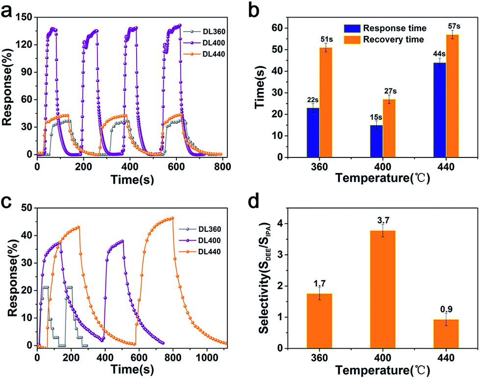 | ||
| Fig. 2 Gas sensing properties of the three DL structures. (a) Response curves and (b) response and recovery times to 100 ppm of DEE at 215 °C. (c) Response curves to 100 ppm of IPA at 215 °C. (d) Selectivity based on the response ratio of DEE to IPA. | ||
We further investigated the selectivity of the DL devices. Among various volatile organic compounds (alcohol, ethers, ketone etc.), the DL devices only show an obvious response to DEE and isopropanol (IPA), thus the selectivity is defined by the sensitivity ratio of DEE to IPA (SDEE/SIPA). As shown in Fig. 2c, the responses of DL360, DL 400 and DL440 are 21%, 38%, 45% to 100 ppm IPA gas at 215 °C. Correspondingly, the selectivity of DL360, DL400 and DL440 are 1.7, 3.7 and 0.9, respectively, and the DL400 presents the best selectivity. Moreover, DL400 is also advantageous on detecting low-concentration DEE, and the response remains detectable (30%) at a DEE concentration as low as 20 ppm (Fig. S3b†).
To investigate the long-term stability of the gas sensor, we measured the response of DL400 to 100 ppm DEE at 215 °C. As shown in Fig. S7,† DL400 exhibited a stable response in the first 12 hours. Then the device was exposed to air for 24 hours, and was measured under the same conditions for 12 hours again. The above testing was repeated for several times, and the performance of the device almost kept constant, indicating very high stability.
The sensing mechanism and selectivity of CdO nanostructures can be understood as below. CdO material is known as a highly conductive oxide, Mott–Schottky analysis indicates a carrier concentration as high as 1020 cm−3 (see Fig. S8† and related calculation), which originates from the numerous oxygen vacancies.19 At the working temperature, DEE molecules are easy to be oxidized via the following reaction
| CH3CH2OCH2CH3 + O2 → CH3CH2OCH(OOH)CH3 | (1) |
The obtained ethyl peroxide possesses high oxidability and binds tightly with oxygen vacancies in CdO nanostructures, as a result, the gas sensors lose electrons and its electrical resistance increase remarkably after being exposed to DEE. In contrast, common volatile organic compounds (VOCs), such as IPA, are reductive, when CdO nanostructures are exposed to VOCs, they can get electrons from VOCs, leading to the decrease of electrical resistance. In this way, the CdO nanostructures can distinguish DEE from common VOCs sensitively.
Nevertheless, three CdO nanostructures exhibit distinct properties. To clarify the origin of the performance difference, we first observed the morphology of the three DL devices. As shown in Fig. 3a and S4a,† N-NFAs kept the contour of Cd NFAs after being oxidized at 360 °C. In contrast, the oxidization at higher oxidation temperature (400 °C) induces many holes in CdO nanoflakes, causing so-called hierarchical holes composed of primary holes surrounded by nanoflakes and secondary holes in nanoflakes (Fig. 3b and S4b†). Further increasing of the oxidization temperature to 440 °C leads to a sponge-like structure (S-structure) (Fig. 3c and S4c†). The formation of holes at higher oxidization temperature arises from the spheroidization of planar nanoflakes due to the spontaneous atomic diffusion, which can reduce the total surface area and free energy.
 | ||
| Fig. 3 Characterizations of CdO nanostructures. Top view SEM images of (a) N-NFAs via the oxidization at 360 °C, (b) P-NFAs via the oxidization at 400 °C, and (c) S-structure via the oxidization at 440 °C. (d) XRD patterns of the three CdO nanostructures. | ||
Second, we measured the specific surface area of three CdO nanostructures by N2 adsorption analysis, and the results were shown in Fig. S5.† The specific surface area of P-NFAs in DL400 (19.6 m2 g−1) is similar to that of N-NFAs in DL360 (18.8 m2 g−1). In contrast, S-structure in DL440 possesses much lower specific surface area (11.6 m2 g−1).
Third, we identified the crystal structures that were considered to make significant impact on gas-sensing properties.18 As shown in Fig. S6a–c,† HRTEM images and SAED patterns illustrate that the three CdO nanostructures are all single crystalline with exposed {111} planes, being consistent with XRD results shown in Fig. 3d. The intensity of (111) peak ascends gradually with the increase of oxidization temperature, and S-structure in DL440 displays the highest (111) peak among the three nanostructures. Based on the above, P-NFAs obtained at 400 °C do not show superiority on either surface area (lower than that of N-NFAs) or exposed crystalline plane (worse than that of S-structure). Therefore, its excellent performance should be ascribed to the unique structure of porous nanoflakes. P-NFAs can provide unimpeded channel for gas flow, facilitate the injection of target gas, thus achieve a better contact and quicker response and recovery than N-NFAs.
On the other hand, when the CdO nanostructures are exposed to air or ethyl peroxide, oxidative molecules can absorb on their surface and seize their electrons, forming a depletion layer. In case of P-NFAs, the secondary holes in nanoflakes introduce additional depletion layer around the holes that is absent in N-NFAs and S-structure. Thus, the ratio of depletion area to total volume of P-NFAs is much larger than the other two structures, which causes higher electrical resistance of P-NFAs, and is responsible for the superior gas sensitivity.
Conclusions
DL devices with different CdO nanostructures on ZnO NRAs are fabricated for DDE detection, and they show obvious advantages over the single layer device consisting of CdO NFAs. Especially, the DL device with P-NFAs exhibits the best gas sensing properties, including the highest sensitivity, the fastest response and recovery, and the highest selectivity. The hierarchical holes in the P-NFAs provide unimpeded channel for gas flow as well as additional depletion layer, which contributes to the superfast response and high sensitivity. These results illuminate that morphology control plays a crucial role in improving the performance of gas sensors, and the novel DL structure with NFAs on NRAs is promising for achieving high performance in other material systems.Acknowledgements
This work was supported by the National Basic Research Program of China (2014CB931703), and the Natural Science Foundation of China (No. 51471115 and 51171127).Notes and references
- (a) J. Bai and B. Zhou, Chem. Rev., 2014, 114, 10131 CrossRef CAS PubMed; (b) P. Feng, F. Shao, Y. Shi and Q. Wan, Sensors, 2014, 14, 17406 CrossRef PubMed.
- (a) Z. Wang, J. Xue, D. Han and F. Gu, ACS Appl. Mater. Interfaces, 2015, 7, 308 CrossRef CAS PubMed; (b) M. Chen, Z. Wang, D. Han, F. Gu and G. Guo, J. Phys. Chem. C, 2011, 115, 12763 CrossRef CAS; (c) Y. Liu, Y. Jiao, Z. Zhang, F. Qu, A. Umar and X. Wu, ACS Appl. Mater. Interfaces, 2014, 6, 2174 CrossRef CAS PubMed.
- (a) X. Zhuang, Y. Mai, D. Wu, F. Zhang and X. Feng, Adv. Mater., 2015, 27, 403 CrossRef CAS PubMed; (b) Y. T. Pan, X. Yin, K. S. Kwok and H. Yang, Nano Lett., 2014, 14, 5953 CrossRef CAS PubMed.
- (a) L. Al-Mashat, K. Shin, K. Kalantar-zadeh, J. D. Plessis, S. H. Han, R. W. Kojima, R. B. Kaner, D. Li, X. L. Gou, S. J. Ippolito and W. Wlodarski, J. Phys. Chem. C, 2010, 114, 16168 CrossRef CAS; (b) X. Xu, H. Li, Q. Zhang, H. Hu, Z. Zhao, J. Li, J. Li, Y. Qiao and Y. Gogotsi, ACS Nano, 2015, 9, 3969 CrossRef CAS PubMed; (c) L. Huang, Z. Zhang, Z. Li, B. Chen, X. Ma, L. Dong and L. M. Peng, ACS Appl. Mater. Interfaces, 2015, 7, 9581 CrossRef CAS PubMed; (d) S. Kumar, S. Kaushik, R. Pratap and S. Raghavan, ACS Appl. Mater. Interfaces, 2015, 7, 2189 CrossRef CAS PubMed; (e) W. Yuan, A. Liu, L. Huang, C. Li and G. Shi, Adv. Mater., 2013, 25, 766 CrossRef CAS PubMed.
- (a) B. Cho, A. R. Kim, Y. Park, J. Yoon, Y. J. Lee, S. Lee, T. J. Yoo, C. G. Kang, B. H. Lee, H. C. Ko, D. H. Kim and M. G. Hahm, ACS Appl. Mater. Interfaces, 2015, 7, 2952 CrossRef CAS PubMed; (b) J. Lee, P. Dak, Y. Lee, H. Park, W. Choi, M. A. Alam and S. Kim, Sci. Rep., 2014, 4, 7352 CrossRef CAS PubMed.
- M. M. Y. A. Alsaif, S. Balendhran, M. R. Field, K. Latham, W. Wlodarski, J. Z. Ou and K. Kalantar-zadeh, Sens. Actuators, B, 2014, 192, 196 CrossRef CAS.
- D. J. Late, T. Doneux and M. Bougouma, Appl. Phys. Lett., 2014, 105, 233103 CrossRef.
- M. O'Brien, K. Lee, R. Morrish, N. C. Berner, N. McEvoy, C. A. Wolden and G. S. Duesberg, Chem. Phys. Lett., 2014, 615, 6 CrossRef.
- J. Ma, J. Zhang, S. Wang, T. Wang, J. Lian, X. Duan and W. Zheng, J. Phys. Chem. C, 2011, 115, 18157 CAS.
- (a) Y. V. Kaneti, J. Yue, X. Jiang and A. Yu, J. Phys. Chem. C, 2013, 117, 13153 CrossRef CAS; (b) X. Wang, W. Liu, J. Liu, F. Wang, J. Kong, S. Qiu, C. He and L. Luan, ACS Appl. Mater. Interfaces, 2012, 4, 817 CrossRef CAS PubMed.
- W. Zeng, M. Wu, Y. Li and S. Wu, J. Mater. Sci.: Mater. Electron., 2013, 24, 3701 CrossRef CAS.
- H. Huang, H. Gong, C. L. Chow, J. Guo, T. J. White, M. S. Tse and O. K. Tan, Adv. Funct. Mater., 2011, 21, 2680 CrossRef CAS.
- (a) X. Fu, J. Liu, T. Han, X. Zhang, F. Meng and J. Liu, Sens. Actuators, B, 2013, 184, 260 CrossRef CAS; (b) W. Sha, P. Gu, B. Zhang and C. Zheng, Mater. Sci. Technol., 2014, 25, 085102 Search PubMed; (c) P. Slobodian, P. Riha, A. Lengalova, P. Svoboda and P. Saha, Carbon, 2011, 49, 2499 CrossRef CAS; (d) Q. Wang, B. Li, Y. Wang, Z. Shou and G. Shi, Luminescence, 2015, 30, 318 CrossRef CAS PubMed; (e) X. Yu, C. Xie, L. Yang and S. Zhang, Sens. Actuators, B, 2014, 195, 439 CrossRef CAS.
- (a) P. F. Yin, T. Ling, Y. R. Lu, Z. W. Xu, S. Z. Qiao and X. W. Du, Adv. Mater., 2015, 27, 740 CrossRef CAS PubMed; (b) Z. L. Zhu, L. Cui, T. Ling, S. Z. Qiao and X. W. Du, J. Mater. Chem. A, 2014, 2, 957 RSC.
- (a) C. Lee, H. B. Cuong, S. H. Jeong and B. T. Lee, J. Alloys Compd., 2015, 645, 322 CrossRef CAS; (b) M. A. Rahman and M. K. R. Khan, Mater. Sci. Semicond. Process., 2014, 24, 26 CrossRef.
- J. Watsont and K. Ihokura, Meas. Sci. Technol., 1993, 4, 711 CrossRef.
- J. H. Lee, Sens. Actuators, B, 2009, 140, 319 CrossRef CAS.
- (a) A. Gurlo, Nanoscale, 2011, 3, 154 RSC; (b) Y. F. Sun, S. B. Liu, F. L. Meng, J. Y. Liu, Z. Jin, L. T. Kong and J. H. Liu, Sensors, 2012, 12, 2610 CrossRef CAS PubMed.
- M. A. Rahman and M. K. R. Khan, Mater. Sci. Semicond. Process., 2014, 24, 26 CrossRef.
Footnote |
| † Electronic supplementary information (ESI) available: The SEM image, XRD spectrum and TEM image of Cd NFAs. Gas response plots and SEM images of the DL devices obtained by varying oxidizing temperature. The SEM and TEM images of the CdO with different nanostructures. See DOI: 10.1039/c5ra24708j |
| This journal is © The Royal Society of Chemistry 2016 |