
Size and distribution control of surface plasmon enhanced photoluminescence and SERS signal in Ag–GaN hybrid systems†
Varun Thakura,
Soumik Siddhantab,
C. Narayanaa and
S. M. Shivaprasad*a
aChemistry and Physics of Materials Unit, Jawaharlal Nehru Centre for Advanced Scientific Research, Jakkur P. O., Bangalore – 560064, India. E-mail: smsprasad@jncasr.ac.in; Fax: +91-80-22082947; Tel: +91-80-22082947
bDepartment of Mechanical Engineering, John Hopkins University, Baltimore, MD, USA
First published on 3rd December 2015
Abstract
In the present experiment, two GaN nanowall network (NWN) samples with different porosity were grown on c-sapphire substrates using plasma assisted molecular beam epitaxy (PA-MBE). Ag nanoparticles were deposited on both the samples using a physical vapour deposition (PVD) system. Annealing the samples at different temperatures resulted in a change in Ag nanoparticle size due to diffusion and Ostwald ripening which had significant effect on the photoluminescence and SERS activity of GaN NWN. It was observed that the photoluminescence yield increased by more than five times in both cases at 200 °C. The SERS activity for thiophenol is higher in the as-deposited case for the sample with higher porosity, but after annealing to 200 °C the activity increased for the sample with lower porosity. It is also interesting to observe that the sample with higher porosity shows SERS signals even after being annealed to higher temperatures. Studies are also done for other analytes such as R6G and BSA. The results are discussed in terms of plasmonic effects of Ag nanoparticles on the excitonic emission from the GaN surface, which is also simulated using 2D-FDTD simulations.
1 Introduction
Coupling of excitonic emission with surface plasmons (SP) of metal nanostructures has been used in recent times as a means to enhance spontaneous emission rate as well as emission efficiency1,2 of semiconductors, which can be potentially useful in high performance optoelectronic devices such as light emitting diodes (LEDs),3,4 laser diodes (LDs) and biomolecular detection.5,6 Okamoto et al.4 had suggested that in order to have an efficient extraction of light from the SP modes, roughening or nanostructuring of metal is useful since it allows the SPs of high momentum to lose the momentum and efficiently couple to the radiated emission. This caused metal nanoparticles to be used instead of films, to increase the emission further. By varying the exciton–plasmon interactions, wavelength dependent biodetection tools can be fabricated which improve the quantification of luminescence intensity in related optical pathways.5 Localized surface plasmon resonance (LSPR) is the driving force behind such interactions, which arises as a consequence of confinement of plasmons in nanoparticles of size much smaller than the wavelength of incident light.7 The resonant frequency of the LSPR depends strongly on several factors, namely size and shape of the nanoparticles, dielectric environment and distance between them; which makes it possible to design nanostructures which interact with a wide range of wavelengths. Tapping into the LSPR gives rise to highly sensitive detection techniques like surface enhanced Raman spectroscopy (SERS). The ability to tune the interparticle distance, size and nanoparticle distribution by controlling the surface morphology and thermal treatment can lead the way for tunable SERS substrates. SERS is a distance dependent phenomenon since the enhancement factor has been calculated to decay as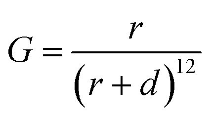 8,9 where r is the radius of the spherical metal structure and d is the distance between the analyte and that structure, thus decreasing the signal enhancement rapidly. The electromagnetic enhancement occurs in conjunction with chemical enhancement, which further increases the detectability by two orders of magnitude. The LSPR based techniques have the capability for identifying down to single molecular level which make them promising detection tools. Specifically, in case of SERS the Raman signal enhancement has been shown to increase by a factor of 106 and more.10
For exploring exciton–plasmon interactions in metal–semiconductor hybrid systems, a broad range of semiconductors have been probed. Since Si is a semiconductor with an established technological application industry, it has attracted a lot of interest. There are reports of electroluminescence being obtained from silicon based devices11 which have been combined with metal nanostructures to exploit exciton–plasmon interactions. However, wide and direct band gap semiconductors are more commonly explored to be used in such structures. GaN is used for fabricating optoelectronic devices for high emission, such as light emitting diodes (LEDs) and laser diodes (LDs) since it is easy to alloy it with Al and In by band gap engineering to obtain devices emitting/absorbing across the solar spectrum and beyond.
GaN based devices have been coated with Ag to enhance internal quantum efficiency3,12 and current collection efficiency in photovoltaics.13 Since surface roughening of GaN is known to improve light extraction,14 it is interesting to study the effect of Ag nanoparticles on the emission properties in its nanostructured morphology. Further, GaN has also been used with Ag nanoparticles to fabricate sensors using SERS.15 Since the emission of GaN in the nanowall form is significantly higher than the traditional flat films16 and can be improved by surface modifications,17 it is desirable to combine the Ag adsorption and enhanced emission capabilities to fabricate multiple usage substrates.
We have previously reported an Ag–GaN system using a novel nanowall network structure of GaN which has shown excellent properties and application as a SERS substrate6 used to sense proteins of both positive and negative surface charges. It was shown that the multiple reflections of the incident radiation due to the morphology of the nanowalls resulted in the enhancement of SERS sensitivity. Although other templates have been explored for SERS application,18 dual use of GaN for enhancement of band edge emission as well as sensing is attractive.
In the present experiment, we extend our previous study by considering variation of porosity of the GaN nanowall structure and its effect on SERS. Further, the size and distance between the Ag nanoparticles is also varied by carrying out annealing at different temperatures, which is known to affect the LSPR frequency of Ag. Apart from the change in SERS signals, the change in plasmon frequency is also harnessed to maximize the band edge emission from GaN which is probed using photoluminescence. It is then interesting to use this substrate not only as a SERS sensor but also as a highly luminescent material whose properties can be tuned by controlling the size and distribution of Ag nanoparticles on its surface. The SERS activity for three different analytes is presented here.
2 Experimental details
Two GaN nanowall network films were grown on bare c-sapphire substrates using a plasma assisted molecular beam epitaxy (PA-MBE) system (SVT, USA). For the first sample S1, the N2 gas flow rate was 6 sccm and the Ga source was maintained at 1000 °C; while for the second sample S2 the corresponding values were 4.5 sccm and 1100 °C, respectively. Thin films of 0.6 μm thickness were grown to form wedge shaped nanowalls in both the cases. The width of the apex of the walls was different in the two cases, and their respective surface coverage were calculated using thresholding technique in Gwyddion (ver 2.34) software.Ag was deposited on the GaN nanowall network samples held at room temperature using electron beam evaporation in a PVD system (SVT, USA) operating at a base pressure of 1 × 10⁻⁹ Torr while the pressure during evaporation was 2 × 10⁻⁶ Torr. The quartz crystal thickness monitor was utilized to estimate the amount of Ag deposited and the thickness in both the cases was 13 nm. Annealing of the samples was carried out in a tube furnace in a nitrogen environment to prevent oxidation. Prior to annealing, the furnace was purged with N2 gas for 20 minutes to evacuate air. The ramp rate of the furnace was 20 °C per minute and the duration of annealing in each case was 1 hour. For both the samples, annealing was carried out at 200 °C and 500 °C. The morphology of the samples was determined ex situ by FESEM (FEI, Netherlands). XPS studies (not shown here) confirm that the Ag nanoparticles are not oxidized during annealing.
The Raman and SERS spectra were recorded using thiophenol as the analyte in the same setup described earlier.19 Optical properties of all the samples were examined by Photoluminescence (PL, Horiba Jobin Yvon) using a Xe lamp source. The excitation wavelength was kept at 325 nm for all measurements using a filter.
Finite difference time domain (FDTD) simulations
2D FDTD simulations (Lumerical Solutions Ltd.) were carried out in order to estimate the electromagnetic field strength around the Ag nanoparticles for both the samples. The simulation region was established using periodic boundary conditions along x- and y- axes and perfectly matched layers along the x-axis. A plane wave polarized light of wavelength range between 400–700 nm was used as the source along the y-axis while the monitor is placed in the z-normal configuration at the center of the nanoparticle group to obtain the maximum signal possible. To get the best resolution while limiting the simulation time, a mesh override region of 3 nm was selected while the simulation time was 2000 fs.3 Results and discussion
Fig. 1(a) and (b) are the plan view FESEM images of samples S1 and S2 respectively, showing typical GaN nanowall network structure, with interconnected walls formed on the surface, though the thickness of the walls was different for both the samples. The higher Ga k-cell temperature employed during the growth of S2 increases the gallium flux on the substrate which leads to thickening of the apex of the walls, as also observed by Zhong et al.20 The reasoning behind this is that in a higher nitrogen rich environment, the Ga adatoms are able to diffuse to only short distances before being nitrided, promoting three dimensional growth. Hence, increasing Ga flux leads to an increase in diffusion lengths of Ga adatoms, thereby increasing the width of the nanowalls. Line scans were performed on the FESEM images in order to obtain an estimate of the thickness of the walls. The average thickness of the walls was 40 and 60 nm for S1 and S2, respectively. Although the values are limited by the resolution of FESEM and fitting parameters, they provide a relative comparison between the surface coverage of the two samples. The estimated surface coverage for S1 is 20% while for S2 it is 50%, thereby providing a much more compact structure in S2. PL spectra of both the samples have been plotted in Fig. 1(c), which shows that S2 has a 20% higher emission than S1, with a narrower FWHM of 117 meV compared to 164 meV for S1, which is attributed to a large density of band tail states.16,21 Although nanowall structures show higher emission than flat films, it has been shown by Zhong et al. that a nanowall structure which has a sharper apex has a lower PL peak intensity and broader FWHM than the structure with thicker apex,20 which is concomitant with our observations. | ||
| Fig. 1 (a), (b) FESEM images showing S1 and S2 GaN nanowall network with different morphologies. All scale bars pertain to 500 nm. (c) Photoluminescence spectra of both the samples. | ||
Fig. 2 compiles the plan view FESEM images of all the samples studied in the present experiment. The images of both the samples reveals the difference in the way that Ag gets deposited on the surface. Since S1 is relatively more porous and the walls are sharper at the apex, most of the Ag is deposited on the sides of the nanowalls. However, due to higher surface coverage of S2 and a thicker apex, most of the Ag is deposited on the flat surface at the top of the walls. In both the cases, the Ag average island sizes are 20 ± 5 nm for S1 and 30 ± 5 nm for S2. Annealing the samples to different temperatures results in an increase of the size of the Ag nanoparticles due to thermally assisted diffusion of the Ag and subsequent Ostwald ripening. The size of the particles for the 200 °C annealed sample for S1 and S2 was 30 and 45 nm, respectively. For the 500 °C annealing case in both the samples the particles grow to a size where they are trapped in the voids between the nanowalls forming large islands with average size 150 nm in both the samples. Since the voids are of different dimensions there is a distribution of large Ag island sizes from 70–300 nm.
 | ||
| Fig. 2 FESEM images showing the morphology of all the Ag-deposited and annealed samples studied in this experiment. From (a)–(c): S1 as-deposited, annealed to 200 °C, annealed to 500 °C; (d)–(f): S2 as-deposited, annealed to 200 °C, annealed to 500 °C. All scale bars pertain to a length of 500 nm. | ||
Fig. 3 shows the PL spectra of S1 and S2 plotted alongside their respective Ag-deposited and annealed samples. The bare and as-deposited samples show similar spectra in both cases, but after annealing to 200 °C, the area under the PL curve increases by 5.3 times the as-deposited case for S1 and 5.7 times for S2. Annealing further to 500 °C reduces the PL for both the samples. In case of S1, the area under the curve is now 1.8 times that of as-deposited PL. However, for S2 the area under the curve is only 0.7 times than the as-deposited sample. The FWHM of the band edge emission for S1 and S2 remains almost unchanged, indicating that only the intensity is modulated appreciably as a function of annealing temperature.
 | ||
| Fig. 3 Photoluminescence spectra of both the samples with Ag-deposited and annealed spectra plotted simultaneously. For both samples S1 and S2, (a) is the bare sample spectrum, (b) is the spectrum taken after as-deposited condition, (c) is after annealing to 200 °C and (d) is after annealing to 500 °C. | ||
Continuing from our previous report on the application of GaN NWN as a SERS active substrate,6 we have carried out SERS on all the samples using thiophenol as the analyte. Fig. 4 shows the SERS enhancement spectra of thiophenol for all the samples in the case of both S1 and S2. It is observed that S2 gave a higher SERS enhancement compared to S1 in the as deposited and 200 °C annealed samples. In the case of 500 °C annealed sample, there was no detectable signal for S2 though S1 still showed some peaks. S1 also shows a reduction in SERS enhancement with annealing of the sample while S2 showed an increase when the sample was annealed to 200 °C. Since the nanoparticles are at their closest in the as deposited configuration for both the samples, the SERS enhancement is expected to be the largest in both samples. The reduction in the SERS signal of S1 when annealed to 200 °C is due to Ag nanoparticles diffusing to form larger nanoparticles and consequently reducing the number of potential hot spot sites on the top surface. However, in S2, due to the flatness of the apex the SERS signal increases because of the reduction in the interparticle distance between the Ag nanoparticles which increases intensity of electromagnetic signals arising between them. The residual signal seen for S1 after being annealed to 500 °C is due to Ag nanoparticles diffusing down the nanowalls and retaining a reasonable interparticle distance, indicating that S1 retains its sensitivity over a much higher range of temperature compared to S2. In case of S2, the particles are too large as compared to S1 and hence no SERS signal is detected. The enhancement factor was calculated for the peak at 1086 cm−1 which corresponds to the in-plane breathing mode coupled to the ν(C–S) mode using the method given by Yu et al.22 Enhancement factor values for all the samples are provided in Table 1.
 | ||
| Fig. 4 SERS spectra of all the samples acquired using thiophenol as analyte. | ||
| Sample name | Enhancement factor |
|---|---|
| Sample 1 as deposited | 9.97 × 10⁴ |
| Sample 1 200 °C | 9.57 × 10⁴ |
| Sample 1 500 °C | 1.06 × 10⁵ |
| Sample 2 as deposited | 4.73 × 10⁵ |
| Sample 2 200 °C | 5.51 × 10⁵ |
In addition to thiophenol, we have performed SERS studies on two biologically relevant analyte molecules, namely Rhodamine 6G and bovine serum albumin (BSA). While R6G is used extensively to label, detect and image biomolecules like nucleotides and proteins,23 the protein BSA constitutes a class of serum albumins used to study drug–ligand interactions.24 The SERS modes of these molecules could be discerned at low (micro and nano) molar concentrations which makes the SERS substrate useful for potential biological applications. The SERS band assignments for R6G and BSA were made according to those reported in the literature.25–27 R6G gives strong SERS signals due to presence of highly polarizable groups (Fig. 5). On the other hand, proteins are complex and bulky molecules which have low Raman scattering cross section. The SERS substrate was able to enhance the BSA Raman signals efficiently and we could observe SERS modes corresponding to the aromatic amino acids phenylalanine, tyrosine, tryptophan and histidine as well as modes from the peptide backbone and aliphatic side chains. We could also observe the amide modes which are a combination of C![[double bond, length as m-dash]](https://www.rsc.org/images/entities/char_e001.gif) O stretching combined with N–H bending vibrations.28 The amide modes (mostly the amide I mode at around 1650 cm−1) are indicative of the secondary structures of proteins and often used to elucidate different structural aspects of the proteins (Fig. 6).29
O stretching combined with N–H bending vibrations.28 The amide modes (mostly the amide I mode at around 1650 cm−1) are indicative of the secondary structures of proteins and often used to elucidate different structural aspects of the proteins (Fig. 6).29
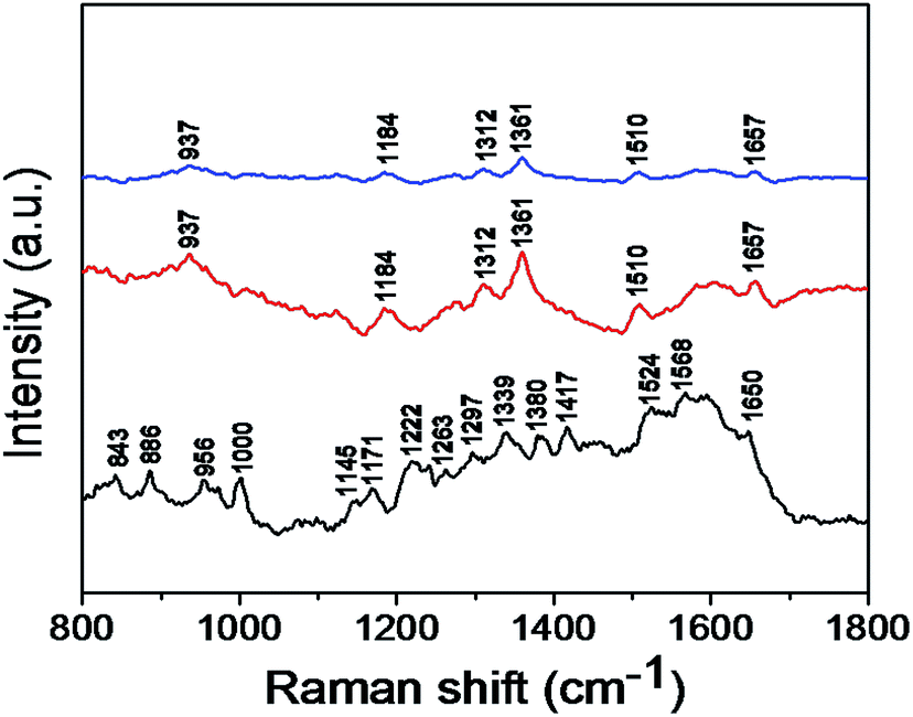 | ||
| Fig. 5 SERS spectra of bovine serum albumin (10−6 M, black) and Rhodamine 6G (10−6 M and 10−9 M in red and blue respectively). | ||
 | ||
| Fig. 6 Zoomed in FESEM images of the as-deposited configuration of (a) sample 1 and (b) sample 2 with corresponding 2D-FDTD simulations using similar interparticle distances. | ||
In order to estimate strength of electromagnetic fields on the surface of the nanoparticle, 2D FDTD simulations have been carried out using the SEM images as a guide for the distribution of Ag nanoparticles on the GaN surface. A representative FDTD calculation done for the as-deposited case is shown in Fig. 5. A higher electromagnetic field strength around the nanoparticles in S2 in comparison to S1 is observed. For S1, the nanoparticles have an interparticle spacing of around ≈50 nm, which gives a much lower electromagnetic field strength compared to S2, where the interparticle spacing reduces to ≈10 nm or lower. The corresponding |E|2 values for the two samples are 219.49 and 60.53 (V m−1)2 respectively. Hence, S2 shows an electromagnetic field 3.6 times stronger than S1. Since in S1 the majority of Ag is deposited on the r-plane sidewalls,30 it is evident that nanoparticles when deposited on the top surface (c-plane) exhibit higher field strengths around them.
It should also be noted that the GaN nanowalls promote light trapping in the form of multiple reflections of the incident light which contributes to the enhancement of electromagetic field in the vicinity of the deposited Ag nanoparticles.6 The interplay of the enhanced reflections combined with the hotspots generated by the Ag nanoparticle aggregates increases the efficacy of the Ag–GaN hybrid SERS substrates.
4 Conclusions
We have studied the luminescence and SERS signals from a large surface area GaN nanowall network by changing the porosity of the surface as well as tuning the size and interparticle distance of the Ag nanoparticles adsorbed on it. Higher photoluminescence as well as enhancement is obtained from the sample with lower porosity, but the quenching of signal is also stronger as annealing to higher temperatures is carried out. The diffusion process occurring due to thermal treatment causes a change in the size of Ag nanoparticles which affects the resultant emission of Ag–GaN system. The maximum emission in our case, obtained at 200 °C, is due to the optimum situation wherein apart from having Ag particles of appropriate size to maximize the resonant emission from GaN, enough area of the semiconductor is left exposed to minimize scattering from the metal electrons. This provides an excellent temperature dependent control on the coupling and consequently the emission characteristics. As seen from the FDTD calculations, the higher electric field intensity around the nanoparticles in S2 gives rise to higher SERS enhancement. Our study shows that while the SERS signals are observed for the structure with higher porosity even after significant separation between Ag nanoparticles, the signals are lost for the surface with lower porosity. However, the surface with lower porosity provides a higher signal in the as-deposited scenario. Therefore, the GaN supported plasmonic silver nanoparticles can be used for sensitive SERS studies related to biomolecules where the surface orientation to the surface of silver nanoparticle plays an important role in spectral interpretations.31 Although the enhancement factor in all the cases is around the previously obtained value of 105, the photoluminescence enhancement at 200 °C shows that the substrate can act as an emission enhancer without losing the SERS sensitivity over a range of temperatures. This enhancement is consistent with the earlier reports of discrete silver nanoparticles with uniform hotspots which is a stepping stone to obtaining reproducible SERS spectra.32 The possibility of combining the plasmonic and the PL enhancements present an interesting approach for the utilization of the substrate for dual purposes.Thus, we have demonstrated a tunable Ag–GaN NWN hybrid system which shows an enhancement in the band edge emission because of surface plasmon coupling to the excitonic emission. In addition, the system can be used as a SERS substrate at various temperatures with differing sensitivity depending on the surface coverage of the film. The two applications shown in this report vary in their sensitivity with temperature, and thus the use of a single hybrid substrate to realize high performance optoelectronic and sensing properties.
Acknowledgements
SMS thanks Prof. CNR Rao for unstinted support and guidance. The authors acknowledge JNCASR for facilities and DST for funding. VT and SS acknowledge DST for senior research fellowship.References
- X. Zhang, P. Wang, X. Zhang, J. Xu, Y. Zhu and D. Yu, Nano Res., 2009, 2, 47–53 CrossRef CAS.
- J. Yoo, X. Ma, W. Tang and G. C. Yi, Nano Lett., 2013, 13, 2134–2140 CrossRef CAS PubMed.
- C. Y. Cho, K. S. Kim, S. J. Lee, M. K. Kwon, H. Ko, S. T. Kim, G. Y. Jung and S. J. Park, Appl. Phys. Lett., 2011, 99, 10–13 Search PubMed.
- K. Okamoto, I. Niki, A. Shvartser, Y. Narukawa, T. Mukai and A. Scherer, Nat. Mater., 2004, 3, 601–605 CrossRef CAS PubMed.
- J. Lee, P. Hernandez, J. Lee, A. O. Govorov and N. A. Kotov, Nat. Mater., 2007, 6, 291–295 CrossRef CAS PubMed.
- S. Siddhanta, V. Thakur, C. Narayana and S. M. Shivaprasad, ACS Appl. Mater. Interfaces, 2012, 4, 5807–5812 CAS.
- E. Hutter and J. H. Fendler, Adv. Mater., 2004, 16, 1685–1706 CrossRef CAS.
- K. Kneipp, H. Kneipp, I. Itzkan, R. R. Dasari and M. S. Feld, Chem. Rev., 1999, 99, 2957–2976 CrossRef CAS PubMed.
- A. Campion and P. Kambhampati, Chem. Soc. Rev., 1998, 27, 241–250 RSC.
- S. Nie, Science, 1997, 275, 1102–1106 CrossRef CAS PubMed.
- R. J. Walters, R. V. A. van Loon, I. Brunets, J. Schmitz and A. Polman, IEEE Int. Conf. Group IV Photonics, 4th, 2009, 9, 74–76 Search PubMed.
- Y. M. Song, E. S. Choi, G. C. Park, C. Y. Park, S. J. Jang and Y. T. Lee, Appl. Phys. Lett., 2010, 97, 10–13 Search PubMed.
- I. M. Pryce, D. D. Koleske, A. J. Fischer and H. A. Atwater, Appl. Phys. Lett., 2010, 96, 1–4 CrossRef.
- T. Fujii, Y. Gao, R. Sharma, E. L. Hu, S. P. DenBaars and S. Nakamura, Appl. Phys. Lett., 2004, 84, 855–857 CrossRef CAS.
- B. Nie, B. K. Duan and P. W. Bohn, J. Raman Spectrosc., 2012, 43, 1347–1353 CrossRef CAS.
- V. Thakur, M. Kesaria and S. M. Shivaprasad, Solid State Commun., 2013, 171, 8–13 CrossRef CAS.
- V. Thakur, S. K. Nayak, K. K. Nagaraja and S. M. Shivaprasad, Electron. Mater. Lett., 2015, 11, 398–403 CrossRef CAS.
- K. D. Alexander, K. Skinner, S. Zhang, H. Wei and R. Lopez, Nano Lett., 2010, 10, 4488–4493 CrossRef CAS PubMed.
- G. Pavan Kumar and C. Narayana, Curr. Sci., 2007, 93, 778 Search PubMed.
- A. Zhong and K. Hane, Nanoscale Res. Lett., 2012, 7, 686 CrossRef.
- H. P. Bhasker, S. Dhar, A. Sain, M. Kesaria and S. M. Shivaprasad, Appl. Phys. Lett., 2012, 101, 132109 CrossRef.
- H.-Z. Yu, J. Zhang, H.-L. Zhang and Z.-F. Liu, Langmuir, 1999, 15, 16–19 CrossRef CAS.
- Y. C. Cao, R. Jin, J.-M. Nam, C. S. Thaxton and C. A. Mirkin, J. Am. Chem. Soc., 2003, 125, 14676–14677 CrossRef CAS PubMed.
- P. Miskovsky, J. Hritz, S. Sanchez-cortes, G. Fabriciova, J. Ulicny and L. Chinsky, Photochem. Photobiol., 2001, 74, 172–183 CrossRef CAS PubMed.
- A. M. Michaels, M. Nirmal and L. E. Brus, J. Am. Chem. Soc., 1999, 121, 9932–9939 CrossRef CAS.
- E. Podstawka, Y. Ozaki and L. M. Proniewicz, Appl. Spectrosc., 2004, 58, 1147–1156 CrossRef CAS PubMed.
- S. Siddhanta, D. Karthigeyan, P. P. Kundu, T. K. Kundu and C. Narayana, RSC Adv., 2013, 3, 4221 RSC.
- A. Barth and C. Zscherp, Q. Rev. Biophys., 2002, 35, S0033583502003815 CrossRef.
- S. Siddhanta and C. Narayana, Nanomater. Nanotechnol., 2012, 2, 1–13 CrossRef.
- M. Kesaria and S. Shivaprasad, Appl. Phys. Lett., 2011, 99, 143105 CrossRef.
- D. Karthigeyan, S. Siddhanta, A. H. Kishore, S. S. R. R. Perumal, H. Agren, S. Sudevan, A. V. Bhat, K. Balasubramanyam, R. K. Subbegowda, T. K. Kundu and C. Narayana, Proc. Natl. Acad. Sci. U. S. A., 2014, 111, 10416–10421 CrossRef CAS PubMed.
- X. Shen, C. M. Ho and T. S. Wong, J. Phys. Chem. B, 2010, 114, 5269–5274 CrossRef CAS.
Footnote |
| † Electronic supplementary information (ESI) available. See DOI: 10.1039/c5ra24906f |
| This journal is © The Royal Society of Chemistry 2015 |