
All-solution-processed, flexible thin-film transistor based on PANI/PETA as gate/gate insulator†
Jin-Yong Honga,
Dai Gun Yoonb,
Byung Doo Chin*b and
Sung Hyun Kim*c
aDepartment of Electrical Engineering and Computer Science, Massachusetts Institute of Technology, 77 Massachusetts Avenue, Cambridge, MA 02139, USA
bDepartment of Polymer Science and Engineering, Dankook University, Youngin 448-701, Republic of Korea. E-mail: bdchin@dankook.ac.kr
cDepartment of Chemistry, College of Natural Sciences, Seoul National University, Seoul 151-747, Republic of Korea. E-mail: shkim75@snu.ac.kr
First published on 9th December 2015
Abstract
Polyaniline (PANI)/pentaerythritol triacrylate (PETA) as gate/gate insulator is introduced to improve the device performance for all-solution-processed organic thin film transistors (TFTs). Direct comparison of the TIPS-pentacene crystal growth patterns on PANI/PETA and on Si/SiO2 as gate/gate insulators is investigated for the origin of different device performances.
Organic thin film transistors (TFTs) are envisaged as the main electronic components in future electronic devices.1 Along with advancements in organic electronics in general, organic TFTs will lead to the development of flexible, shatterproof, light-weight, and highly portable displays, like those in future-generation smart phones and tablet PCs, by enabling flexible pixel-switching devices. However, the use of inorganic materials for gate/gate insulators has been a main obstacle in realizing bendable and flexible form factors. It is therefore important to identify various materials that can be used as alternative flexible electrodes. Among the various materials that have been suggested, polyaniline (PANI) is considered as a promising candidate for low-cost and flexible electrodes in organic TFTs because of its high conductivity, solution processability, long-term stability, and superior mechanical flexibility.2 Secondary doping of PANI with camphorsulfonic acid (CSA) in m-cresol makes this polymer highly-conductive and appropriate for use as thin-film electrodes on various substrates.3 In terms of the gate insulators for organic TFTs, the material should have the functions such as abrasion resistance for subsequent solution deposition, good contact with neighbour materials, and water resistance for ambient fabrication condition.
In this study, we fabricated organic TFTs with 6,13-bis(triisopropylsilylethynyl)-pentacene (TIPS-pentacene) as an organic semiconductor, CSA-doped PANI as a gate electrode, and cross-linked pentaerythritol triacrylate (PETA) as a gate insulator. Polyethersulfone (PES) as a plastic substrate and silver (Ag) as source and drain electrodes were employed for all-solution-processed TFTs. The TIPS-pentacene was chosen as a representative organic semiconductor because of its high mobility, air stability, and solution processability.4 Particularly, CSA-doped PANI and PETA are highly compatible with the PES substrate, exhibiting good wettability, which provides mechanical stability and flexibility. We correlate the device performance to the morphology of the semiconductor on the gate insulator between PETA and SiO2. The resulting PANI/PETA gate/gate insulator device produced a higher mobility than the Si/SiO2 device. This was attributed to the large crystal domains in the surface morphology of TIPS-pentacene on the PETA gate insulator.
As shown in Fig. 1a, bottom-gate bottom-contact TIPS-pentacene TFT consisted of printed Ag source/drain electrodes on a cross-linked polymer gate insulator/CSA-doped PANI gate electrode which was spin-coated on a PES substrate. For comparison, we also fabricated reference TFT with Si/SiO2 as gate/gate insulator in the identical configuration (Fig. S1, ESI†). The PANI gate adhered strongly to the PES and was in intimate contact (Fig. 1c), resulting in a gate electrode on the substrate that was mechanically stable with regard to bending and folding condition. The PANI gate electrode (∼700 nm thick), having macroporous structure originating from its intrinsically fibrous morphology (Fig. S2, ESI†),5 showed a very low sheet resistance of 60 Ω sq−1 measured by 4-point probe system.
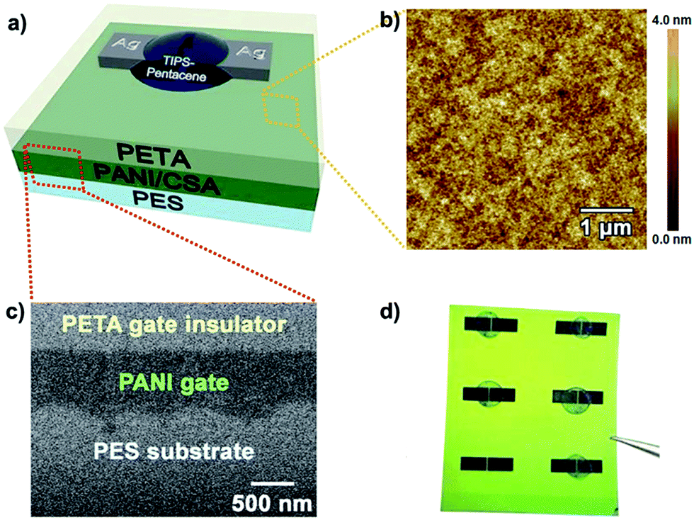 | ||
| Fig. 1 (a) Schematic device configuration of the bottom-gated TIPS-pentacene TFT consisted of the PANI/PETA as the gate/gate insulator. (b) AFM image of a PETA gate insulating layer. (c) Cross-sectional SEM image consisting of a CSA-doped PANI gate and a PETA gate insulator on a PES substrate. (d) Photograph of as-prepared TIPS-pentacene TFTs. | ||
In this study, we adopt the PETA material as a gate insulator. It has been reported that the most commonly used gate insulator materials (e.g. poly(4-vinylphenol) (PVP) and poly(vinyl alcohol) (PVA)) are too sensitive to be employed in the device fabrication with ambient atmosphere due to oxygen and moisture. The performance of TFTs often degrades when the devices are exposed to air and moisture. It has been known that the PETA is a suitable material for a gate insulator material due to its ease in handling and processing, chemical resistance, and low volatility under ambient condition of the TFT fabrication process. The PETA film formation was successfully completed with UV-curing after spin-coating process within very short time (<60 s). All procedures were performed at room temperature in a glove box that provided oxygen-free conditions. The conversion value (degree of curing) of the as-prepared PETA film was estimated as 99.3%, indicating high crosslinking yield. In addition, the root-mean-square (RMS) roughness of the PETA layer was 0.786 nm and the film thickness is about 750 nm by AFM (Fig. 1b, S3 and S4, ESI†).
Fig. 1d illustrated the photographic images of PANI/PETA-based TFTs. Rectangular Ag source/drain electrodes (1.5 mm width and 3.0 mm length) were constructed on the cross-linked gate insulator film using an inkjet printer with a channel length of 100 μm. Drop-casted TIPS-pentacene semiconductor on the inkjet-printed channel showed radial growth patterns of crystallites.
Fig. 2 describes the electrical output and transfer characteristics of PANI/PETA-based TFTs. Most importantly, the calculated mobility of the PANI/PETA TFTs was roughly 6 times higher than that of the Si/SiO2 TFTs (Table 1 and Fig. S5, ESI†). A Gaussian fit in Fig. S6† indicates the carrier mobility values of 0.109 ± 0.02 and 0.019 ± 0.01 cm2 V−1 s−1 for PANI/PETA-based and Si/SiO2-based TFT devices, respectively. The output curves from both TFTs are S-shaped in the linear region in Fig. 2. These curve patterns can be attributed to the contact resistance between TIPS-pentacene and Ag.6 As mentioned it above, the PETA has a relatively higher roughness value than that of Si/SiO2 surface (the roughness of thermally grown bare SiO2 was known as ∼0.2 nm in the literatures).7 Charges transport along rough surfaces are more vulnerable to trapping, while smooth surface assists charges transport at the interface.8 Thus, the rough surface of the PETA layer can be another reason for more inclined S-shaped output curve in the PANI/PETA device (Fig. 2a).
 | ||
| Fig. 2 (a and b) Source–drain current versus drain voltage characteristics of the TIPS-pentacene OTFTs with the PANI/PETA as gate electrode/gate insulator at gate voltages from 0 to −50 V. (b) Source–drain current versus gate voltage at VDS = −50 V for the TIPS-pentacene OTFTs with the PANI/PETA as gate electrode/gate insulator. | ||
Despite the disadvantages of the rougher surface of PETA, the PANI/PETA devices exhibited enhanced mobility compared to that of Si/SiO2 devices. In general, the mobility in semiconductors depends on the size and quality of the crystalline domains, which can be affected by deposition conditions and the nature of the insulator surface.9 We therefore hypothesized that the origin of high mobility in these PANI/PETA-based TFTs is associated with the crystal growth pattern of TIPS-pentacene on the gate insulator. Many researchers have employed self-assembled monolayers over SiO2 gate insulators to improve the molecular ordering of the polymeric semiconductor. In general, this resulted in increased mobility over bare SiO2.10 In this study, however, surface modification of the gate insulators was avoided in order to allow a direct comparison of crystal growth pattern on PETA and on bare SiO2. The growth patterns of the semiconductor on both PANI/PETA and Si/SiO2 were investigated, and correlated to device performance.
In Fig. 3a and b, optical microscope images show the crystal structures in the channel area of PANI/PETA TFTs. It can be easily observed that the morphology of TIPS-pentacene is largely dependent on that of the underlying layer. In order to gain insight of the morphology in the channel region, the AFM analysis was conducted. The AFM images proved that the differences in the crystal growth pattern of the TIPS-pentacene depended on differences in the gate insulator (Fig. S7, ESI†). In both PANI/PETA and Si/SiO2 TFTs, we can distinguish three different regions along the transistor channel: a center region, a transition region, and an outer region, respectively. In particular, the morphologies of the transition regions of the PANI/PETA and Si/SiO2 TFTs are significantly different. Akkerman et al. reported that the TIPS-pentacene channel was divided into different regions according to morphology where the largest field-effect mobility was observed in the transition region.11 As presented in Fig. 3c and S7e,† the width of the narrow elongated crystalline domains on PANI/PETA is larger than that on Si/SiO2. We believe that this morphological difference is a dominant factor in enhancing the mobility of the PANI/PETA TFTs over that of Si/SiO2 TFTs. The crystalline domains can be, moreover, identified with the interaction between non-polar TIPS-pentacene molecules and the surface of gate insulator. Water contact angle measurement revealed that the surface of the PETA (Fig. 3d), which was modified by the UV-curing process during the film forming, was more polar than that of SiO2 in Fig. S8.† The molecules of TIPS-pentacene can be attracted each other readily away from the polar surface of the PETA layer, increasing the size of the crystal domain. However, non-polar surface of the SiO2 layer reduce the molecular packing of the organic semiconductor due to the pinning interaction between the SiO2 surface and the TIPS-pentacene molecules, decreasing the crystal domain size.12 It also has been known that the polar interface of gate insulator induces the broadening of the density of states so that more trap states hinder the carrier transport.13 However, it is believed that the crystal orientation-dependent morphology is more critical factor when determining the device performances, rather than carrier trapping effect by the polar surface of the gate insulator. Consequently, deposition of TIPS-pentacene onto the relatively polar surface of PETA resulted in the growth of large crystal domains compared to those grown on the non-polar surface of the SiO2 gate insulator. The narrowness of the crystalline domains in Si/SiO2 TFTs may result in a large resistance between crystalline domains in the channel, thereby decreasing carrier mobility.
 | ||
| Fig. 3 (a) Optical microscope images of channel area in PANI/PETA-based TFTs. Dashed red areas in (a) is enlarged to (b). (c) AFM images of TIPS-pentacene in the channel area of TFTs. (d) Optical images of water droplet on the surface of the PANI/PETA substrate. | ||
Furthermore, the cyclic bending test was performed to demonstrate the flexibility of the fabricated devices. The bending tests were performed using a home-made bending machine with bending radius of 20 mm. In Fig. 4, there is little change in normalized mobility over 1000 cycles. The initial mobility (0.11 cm2 V−1 s−1) of the PANI/PETA-based TFT device was preserved by 95.4% (0.10 cm2 V−1 s−1) even though there is a slight fluctuation, indicating superior flexibility and long-term durability of the PANI/PETA-based TFT devices.
 | ||
| Fig. 4 A change in normalized mobility of the PANI/PETA-based TFT during 1000 times of bending cycles. The bending tests were performed using a home-made bending machine with bending radius of 20 mm. | ||
Conclusions
In summary, PANI/PETA as gate/gate insulator was prepared by consecutive spin-coating of PANI and UV-cured PETA onto a PES substrate. This gate/gate insulator was incorporated into TIPS-pentacene TFTs through all-solution processing in an ambient atmosphere. Differences in the crystal growth pattern of TIPS-pentacene on different gate insulators were attributed to the polarity of the surfaces. Large crystalline domains enhanced carrier mobility in PANI/PETA-gated TIPS-pentacene TFTs. This result presents a practical strategy for the fabrication of high-performance, all-solution-processed, flexible electronic devices by introducing a highly conductive and flexible PANI/PETA gate/gate insulator.Acknowledgements
This research was supported by Leading Foreign Research Institute Recruitment Program (2010-00525) and Mid-career Research Program (2015R1A2A2A04006172) through the National Research Foundation (NRF) of Korea funded by the MEST.Notes and references
- (a) S. Ju, A. Facchetti, Y. Xuan, J. Liu, F. Ishikawa, P. Ye, C. Zhou, T. J. Marks and D. B. Janes, Nat. Nanotechnol., 2007, 2, 378 CrossRef CAS PubMed; (b) C. Wang, J. Zhang, K. Ryu, A. Badmaev, L. G. de Arco and C. Zhou, Nano Lett., 2009, 9, 4285 CrossRef CAS PubMed; (c) J. Zhang, C. Wang and C. Zhou, ACS Nano, 2012, 6, 7412 CrossRef CAS PubMed; (d) G. Schwartz, B. C.-K. Tee, J. Mei, A. L. Appleton, D. H. Kim, H. Wang and Z. Bao, Nat. Commun., 2013, 4, 1859 CrossRef PubMed.
- R. V. Salvatierra, C. E. Cava, L. S. Roman and A. J. G. Zarbin, Adv. Funct. Mater., 2013, 23, 1490 CrossRef CAS.
- (a) A. G. MacDiarmid and A. J. Epstein, Synth. Met., 1994, 65, 103 CrossRef CAS; (b) A. G. MacDiarmid and A. J. Epstein, Synth. Met., 1995, 69, 85 CrossRef CAS; (c) S. H. Park, K.-H. Shin, J.-Y. Kim, S. J. Yoo, K. J. Lee, J. Shin, J. Jang and Y.-E. Sung, J. Photochem. Photobiol., A, 2012, 245, 1 CrossRef CAS.
- (a) D. H. Kim, D. Y. Lee, H. S. Lee, W. H. Lee, Y. H. Kim, J. I. Han and K. Cho, Adv. Mater., 2007, 19, 678 CrossRef CAS; (b) C. W. Sele, B. K. C. Kjellander, B. Niesen, M. J. Thornton, J. B. P. H. van der Putten, K. Myny, H. J. Wondergem, A. Moser, R. Resel, A. J. J. M. van Breemen, N. van Aerle, P. Heremans, J. E. Anthony and G. H. Gelinck, Adv. Mater., 2009, 21, 4926 CrossRef CAS PubMed; (c) S. K. Park, D. A. Mourey, J. I. Han, J. E. Anthony and T. N. Jackson, Org. Electron., 2009, 10, 486 CrossRef CAS; (d) S. S. Zade, N. Zamoshchik, A. R. Reddy, G. Fridman-Marueli, D. Sheberla and M. Bendikov, J. Am. Chem. Soc., 2011, 133, 10803 CrossRef CAS PubMed.
- J. Huang and R. B. Kaner, Angew. Chem., Int. Ed., 2004, 43, 5817 CrossRef CAS.
- K.-H. Shin, J. Cho, J. Jang, H. S. Jang, E. S. Park, K. Song and S. H. Kim, Org. Electron., 2012, 13, 715 CrossRef CAS.
- (a) S. Steudel, S. D. Vusser, S. D. Jonge, D. Janssen, S. Verlaak, J. Genoe and P. Heremans, Appl. Phys. Lett., 2004, 85, 4400 CrossRef CAS; (b) S. E. Fritz, T. W. Kelley and C. D. Frisbie, J. Phys. Chem. B, 2005, 109, 10574 CrossRef CAS.
- (a) W. L. Yang, T. S. Chao, C.-M. Cheng, T. M. Pan and T. F. Lei, IEEE Trans. Electron Devices, 2001, 48, 1304 CrossRef CAS; (b) A. Hossain, A. E. Bolotnikov, G. S. Camarda, Y. Cui, S. Babalola, A. Burger and R. B. James, J. Electron. Mater., 2008, 37, 1356 CrossRef CAS.
- (a) J. Chen, C. K. Tee, M. Shtein, D. C. Martin and J. Anthony, Org. Electron., 2009, 10, 696 CrossRef CAS; (b) R. Z. Rogowski, A. Dzwilewski, M. Kemerink and A. A. Darhuber, J. Phys. Chem. C, 2011, 115, 11758 CrossRef CAS.
- (a) M. Halik, H. Klauk, U. Zschieschang, G. Schmid, C. Dehm, M. Schütz, S. Malsch, F. Effenberger, M. Brunnbauer and F. Stellacci, Nature, 2004, 431, 963 CrossRef CAS PubMed; (b) S. Kobayashi, T. Nishikawa, T. Takenobu, S. Mori, T. Shimoda, T. Mitani, H. Shimotani, N. Yoshimoto, S. Ogawa and Y. Iwasa, Nat. Mater., 2004, 3, 317 CrossRef CAS; (c) K. P. Pernstich, S. Haas, D. Oberhoff, C. Goldmann, D. J. Gundlach, B. Batlogg, A. N. Rashid and G. Schitter, J. Appl. Phys., 2004, 96, 6431 CrossRef CAS; (d) M. McDowell, I. G. Hill, J. E. McDermott, S. L. Bernasek and J. Schwartz, Appl. Phys. Lett., 2006, 88, 073505 CrossRef; (e) M. Park, J. Jang, S. Park, J. Kim, J. Seong, J. Hwang and C. E. Park, Appl. Phys. Lett., 2012, 100, 102110 CrossRef.
- H. B. Akkerman, H. Li and Z. Bao, Org. Electron., 2012, 13, 2056 CrossRef CAS.
- (a) B. J. Song, K. Hong, W.-K. Kim, K. Kim, S. Kim and J.-L. Lee, J. Phys. Chem. B, 2010, 114, 14854 CrossRef CAS PubMed; (b) S. Nam, D. S. Chung, J. Jang, S. H. Kim, C. Yang, S.-K. Kwon and C. E. Park, J. Electrochem. Soc., 2010, 157, H90 CrossRef CAS.
- J. Veres, S. D. Ogier, S. W. Leeming, D. C. Cupertino and S. M. Khaffaf, Adv. Funct. Mater., 2003, 13, 199 CrossRef CAS.
Footnote |
| † Electronic supplementary information (ESI) available: Experimental details, electrical characteristics, and AFM surface images. See DOI: 10.1039/c5ra23848j |
| This journal is © The Royal Society of Chemistry 2015 |