
SnS2 nanosheet-based microstructures with high adsorption capabilities and visible light photocatalytic activities†
Zhengcui Wu*ab,
Yejing Xuea,
Yali Zhanga,
Jingjing Lia and
Tao Chen*b
aAnhui Key Laboratory of Molecule-Based Materials, The Key Laboratory of Functional Molecular Solids, Ministry of Education, College of Chemistry and Materials Science, Anhui Normal University, Wuhu 241000, P. R. China. E-mail: zhengcui@mail.ahnu.edu.cn; Fax: +86 553 3869302; Tel: +86 553 3869302
bDepartment of Physics, The Chinese University of Hong Kong, Shatin, N.T., Hong Kong, China. E-mail: taochen@phy.cuhk.edu.hk
First published on 2nd March 2015
Abstract
The engineering of semiconductors with high adsorption and visible light-driven photocatalytic activity is of growing interest in the removal of environmental pollutants. Herein, SnS2 nanosheet-based microstructures of flower-like, nanosheet-like, nest-like and nanoplate-like morphologies with high adsorption capacities and visible light photocatalytic activities were experimentally achieved by a facile solution-phase approach based on a simple reaction of SnCl4·5H2O and three hydration sodium diethyldithiocarbamate (C5H10NS2Na·3H2O) in a solvent of ethylene glycol with or without the addition of acetic acid, where C5H10NS2Na·3H2O served as both a sulfur source and a coordination agent. The negatively charged nature of the as-prepared SnS2 products is responsible for the superior absorptive and visible light photocatalytic performances of cationic dyes. The revelation of the charged nature of the surface of SnS2 nanosheet-based microstructures leads to a new possibility for the design of adsorptive photocatalysts.
Introduction
The efficient disposal of environmental pollutants is a major challenge for the sustainable development of modern society due to the inverse impacts of industrialization. Among various remediation technologies, adsorption and photocatalytic degradation of chemically stable organic pollutants occupy a prominent place because of some obvious advantages, such as cost-effectiveness, ease of operation and high efficiency.1,2 Comparatively, photocatalytic degradation with a catalyst is a more attractive technology because the organic pollutants can be completely mineralized into CO2, H2O and inorganic substances, without leaving any harmful residues.3 In view of the omnipresent existence of semiconductor minerals, the photodegradation of environmental organic compound, particularly the organic pollutants in water became possible through constructing stable and efficient photochemical systems, which has emerged as a promising technique for disposing wastewaters containing low-concentration organic dye pollutants.4 The photocatalytic decomposition of pollutants in real applications for water decontamination requires the use of non-toxic, affordable and reproducible materials. Moreover, the visible light-driven photocatalysts are more potential, which can absorb visible light that accounts for about 43% of the solar spectrum. On various frontiers for activity-enhanced visible light photocatalysis, surface/interface and structure tuning strategies for the semiconductor with large band gap such as TiO2, ZnO, which can primarily make use of UV light with about 4% of the total sunlight, have progressed at a fast pace, such as constructing heteronanostructure or composite by coupling narrow band gap semiconductor5–11 or noble metal with plasmon resonance in visible light region,12–17 and doping with metal or non-metal element,18–23 where the energetics and interfacial charge-transfer processes can be influenced in a favorable way. However, the fabrications are still experimentally difficult because the self-nucleation of the secondary nanostructure or undesired impurity is difficult to be completely avoided, even if employing a two-step reaction process. Therefore, great interest has emerged in one-step synthesis of single-component visible-light driven photocatalyst with a narrow band gap,24–33 where the photocatalytic activity can be improved by structural and morphological innovations.As is known, the adsorption of the pollutants on the catalyst's surface is an essential process for photocatalytic oxidation. Engineering the photocatalyst with high adsorption capability will not only enhance its photocatalytic performance but also extend its practical application for efficiently decreasing the concentration of pollutants in the dark or under the irradiation of weak light.34 Therefore, the adsorptive photocatalyst with both high adsorption capability and photocatalytic activity is exciting for highly active removal of organic pollutants. However, it was generally realized by coupling two kinds of different materials with individually adsorptive and photocatalytic property,35–37 a single component photocatalyst with both high adsorption capacity and photocatalytic activity is rarely reported.
Very recently, quasi-two-dimensional materials have attracted intensive attention because of their exotic electronic properties and high specific surface areas, which bring about potentially excellent applications in optoelectronics, energy storage, catalysis, sensing, etc.38 As one of the most important metal-sulfide materials, SnS2 has a peculiar CdI2-type layered structure consisting of tin atoms sandwiched between two layers of hexagonally disposed close-packed sulfur atoms, which possesses a visible-light band gap of about 2.2–2.35 eV.39,40 Moreover, SnS2 is nonpoisonous, low-cost, chemically stable in acidic or neutral aqueous solutions, and therefore has potential to be a promising visible light-driven photocatalyst for organic pollutant degradation.27–31
During the past decade, there have been extensive efforts to optimize synthesis strategies in solution phase for structural-modulated synthesis of SnS2 nanostructures for a variety of applications. For example, nanoplatelets,28 nanocrystals,41 flower-shaped nanostructures,42 and hollow spheres43 were obtained by addition of surfactant or coordinated agent, while porous SnS2 architectures,29 plate-like nanostructures,44 nanosheets,45 and flowerlike spheres30 were acquired without addition of surfactant or coordinated agent. In addition, nanosheet arrays were synthesized directly on Sn foil by biomolecule-assisted method,31 and freestanding SnS2 single-layers were achieved through a scalable liquid exfoliation.46 However, there were rarely reports so far to provide simple control over various SnS2 nanostructures to disclose the important correlation between the microstructure and the photocatalytic property. Moreover, few researches concerned about the adsorption capacity of the SnS2 nanostructure before photocatalysis.29 From the viewpoints of both fundamental science and practical applications, it will be very attractive to explore the SnS2 nanostructures with both high adsorption capacity and photocatalytic activity. Herein, a series of adsorptive photocatalysts of SnS2 nanosheet-based microstructures with flower-like, nanosheet-like, nest-like and nanoplate-like morphologies were synthesized by a facile solution-phase approach based on a simple reaction of SnCl4·5H2O and C5H10NS2Na·3H2O in the solvent of ethylene glycol with or without addition of acetic acid. The as-prepared SnS2 microstructures showed high adsorption capacities and visible light-driven photocatalytic degradation activities of cationic organic pollutants, which are related with the negatively charged surface of the photocatalysts.
Experimental section
Synthesis of SnS2 nanosheet-based microstructures
All chemicals were of analytical grade and used as received without further purification. In a typical synthesis, a certain amount of C5H10NS2Na·3H2O was dissolved in 30 mL of ethylene glycol, then 1 mmol of SnCl4·5H2O was added. After 10 min of agitation, the mixture was transferred into a Teflon-lined stainless steel autoclave of 50 mL capacity and heated at 160 °C for 12 h and then cooled to room temperature naturally. The resulting yellow precipitate was collected by centrifugation and washed with deionized water and ethanol several times to remove residual ions, and dried at 50 °C for 6 h for further characterization. For flower-like and nanosheet-like SnS2 products, the amount of C5H10NS2Na·3H2O was 1.5 mmol and 2 mmol, respectively. For nest-like and nanoplate-like SnS2 products, the amount of C5H10NS2Na·3H2O was individually 1.5 mmol and 2 mmol, and the solvent was 25 mL of ethylene glycol and 5 mL of acetic acid. The detailed synthetic conditions have been listed in Table S1.†Characterization
Powder X-ray diffraction patterns (XRD) were recorded on a Shimadzu XRD-6000 diffraction system with high-intensity Cu Kα radiation. Field-emission scanning electron microscope (FESEM) images were obtained on a Hitachi S-4800 operated at an accelerating voltage of 5.0 kV. Transmission electron microscopy (TEM) images were taken on a JEOL 2010 operated at an accelerating voltage of 200 kV. UV-visible diffuse reflectance spectra were carried out on a Shimadzu UV-2450 spectrophotometer using magnesium oxide as a standard. Brunauer–Emmett–Teller (BET) nitrogen adsorption–desorption was measured using a Micromeritics NOVA 2000e accelerated surface area and porosimetry system.Adsorptive and photocatalytic measurements
The adsorptive and photocatalytic performances of the SnS2 nanosheet-based microstructures were evaluated by measuring the adsorption and photocatalytic degradation of different pollutants (two cationic dyes of methylene blue (MB) and rhodamine B (RhB), an anionic dye of Methyl Orange (MO), and a colorless organics of phenol) in the dark and then under visible light irradiation, respectively. Typically, 10 mg of the catalyst was dispersed into 150 mL of 2.5 × 10⁻⁵ M pollutant aqueous solution by constant stirring and maintained in the dark for 60 min to reach an adsorption–desorption equilibrium of the pollutant on the catalyst surface. Then, visible light irradiation was carried out using a 300 W Xe lamp with a cutoff filter (λ > 420 nm) (CEL-HXF300, Beijing). At a given time interval, about 3 mL of suspension was withdrawn and analyzed after removal of catalyst particles by centrifugation. The pollutant concentration of the separated solution was analyzed by a UV-vis spectrophotometer (Shimadzu UV-2550, Japan) through checking the characteristic absorbance spectra.Results and discussion
Morphology and structure of SnS2 nanosheet-based microstructures
Various SnS2 nanosheet-based microstructures can be synthesized through controlling the amount of C5H10NS2Na·3H2O with or without addition of acetic acid, as shown in the FESEM images in Fig. 1. When 1.5 mmol of C5H10NS2Na·3H2O was used, the product was large-scale flower-like microspheres with average diameter of 1.5 μm interconnected by nanosheets (Fig. 1a and b, named sample 1). Careful observation can find these nanosheets are composed of smaller nanosheets. When the amount of C5H10NS2Na·3H2O was increased to 2 mmol, SnS2 nanosheets with average diameter of 500 nm were obtained as shown in Fig. 1c and d (named sample 2), of which the high-magnification FESEM image in Fig. 1d clearly unveils the nanosheets are constituted by smaller nanosheets. Interestingly, the tiny SnS2 nanosheets assembled spontaneously into nest-like microspheres with average diameter of 800 nm (Fig. 1e and f, named sample 3), when 1.5 mmol of C5H10NS2Na·3H2O and 5 mL of acetic acid were added. While nanoplate-like SnS2 with average diameter of 200 nm was obtained with 2 mmol of C5H10NS2Na·3H2O and 5 mL of acetic acid (Fig. 1g and h, named sample 4). The results reveal this facile solution-phase approach was successful in obtaining various SnS2 nanosheet-based microstructures, of which the shape and size of the samples were listed in Table S1.† | ||
| Fig. 1 The low- and high-magnification FESEM images of the SnS2 nanosheet-based microstructures. (a and b) sample 1, (c and d) sample 2, (e and f) sample 3, (g and h) sample 4. | ||
 | ||
| Fig. 2 XRD patterns of as-prepared SnS2 nanosheet-based microstructures. (a) sample 1, (b) sample 2, (c) sample 3, (d) sample 4. | ||
The crystallinity and phase purity of the SnS2 nanosheet-based microstructures were further revealed by XRD analysis. As shown in Fig. 2, the XRD patterns all could be perfectly indexed to hexagonal phase SnS2 with good crystallinity (JCPDS no. 83-1705). No impurity diffraction peaks from other phases were detected, indicating the high purity of the products.
The morphology and structure of as-synthesized SnS2 products were further characterized by TEM measurements. Fig. 3a displays the TEM image of sample 1, revealing it was flower-like structure made up of nanosheets. The HRTEM image in Fig. 3b taken on a piece of extended nanosheet of this flower clearly indicates its polycrystalline nature, clarifying it was assembled by smaller nanounits, of which the planar spacing about 0.32 nm corresponded to the (100) plane of hexagonal SnS2. The TEM image in Fig. 3c exhibits sample 2 is nanosheet-like structure constituted of tiny nanosheets, and the fringes' spacing measured ca. 0.32 nm from the HRTEM image in Fig. 3d can be indexed to the (100) lattice spacing of hexagonal SnS2. The TEM investigation of sample 3 showed the tiny nanosheets are well oriented to a hollow sphere-like structure, where obvious contrast between the dark edge and the relatively bright center clearly confirmed its hollow nature. The lattice fringe spacing about 0.32 nm shown in the HRTEM image of Fig. 3f identifies the (100) lattice plane of hexagonal SnS2. The TEM image in Fig. 3g reveals sample 4 was nanoplate-like structure assembled by tiny nanosheets, and the observed fringe spacing of 0.32 nm in the HRTEM image of Fig. 3h verifies a separation of the (100) lattice plane of hexagonal SnS2.
 | ||
| Fig. 3 TEM and HRTEM images of the SnS2 nanosheet-based microstructures. (a and b) sample 1, (c and d) sample 2, (e and f) sample 3, (g and h) sample 4. | ||
To better understand the growth processes of the SnS2 nanosheet-based microstructures accurately, it is necessary to investigate the morphologies of the intermediates at different stages of the reaction. Herein, two intermediates of each sample with corresponding hydrothermal durations of 2 and 4 h were collected for observation, and their FESEM images are shown in Fig. S1.† After 2 h, the products composed of nanoparticles with diameters of about 16 nm for sample 1 to 3 and 28 nm for sample 4 were observed, as shown in Fig. S1a–d.† Careful observation can find these nanoparticles tend to orient into nanosheets. Fig. S1e–h† display the images of each sample reacted for 4 h, revealing that the intermediate was flower-like product with diameter about 800 nm composed of a few nanosheets and accompanied by some tiny nanosheets with lateral size about 100 nm for sample 1, while nanosheet-like product with average lateral size of 380 nm for sample 2, nest-like product with diameter about 700 nm constituted by sparse nanosheets for sample 3, and nanoplate-like product with average lateral size of 170 nm for sample 4. Careful observation can find the nanosheets in these intermediates were all assembled by smaller nanosheets. The intermediates at 2 and 4 h were all determined as hexagonal phase SnS2 by XRD characterization (Fig. S2†). As the reaction time prolonged to 12 h, the final products with larger and denser nanosheet-based microstructures were observed, as learned from the FESEM images shown in Fig. 1. The series of images clearly show that, as the reaction progressed, the initially formed SnS2 nanoparticles were oriented into tiny nanosheets, and further oriented into nanosheet-based microstructures. It should be noted if the reaction time was lower than 2 h, the quantity of the product is too low to be collected for further characterization.
In this approach, the formation of SnS2 nanosheet-based microstructure is through the reaction of Sn4+ with three hydration sodium diethyldithiocarbamate in the solvent of ethylene glycol with or without addition of acetic acid. However, what role does sodium diethyldithiocarbamate play in terms of controlling crystal growth? At elevated temperature, sodium diethyldithiocarbamate can decompose into carbon disulfide, diethylamine and Na+, of which carbon disulfide can serve as the sulfur source to produce SnS2 crystal seeds and tiny 2D nanosheets gradually formed at the expense of the small crystal seeds due to the inherent layer structure. The diethylamine can preferentially bond on the SnS2 surface perpendicular to (001) facet through a lone pair of electrons on nitrogen atom with surface Sn4+ ions, which lead to the confined growth along the [001] direction and induced the tiny SnS2 nanosheets oriented into large 2D nanosheets. The similar ammonia molecules induced mechanism has been clarified in the formation of ZnSe nanosheets.5 As the reaction time increased, the nanosheets can curl and form 3D nanostructures at suitable concentration of sodium diethyldithiocarbamate. When acetic acid was added into the system, it promoted the decomposition of sodium diethyldithiocarbamate, thus formed more diethylamine molecules adsorbed on the surface of tiny SnS2 nanosheets, resulting in larger interspace among the assembled units of tiny nanosheets. In addition, the solvent of ethylene glycol also plays important roles in the formation of the SnS2 nanosheet-based microstructures. On one hand, it can suppress the hydrolyzation of Sn4+ to form SnO2, which is a common reaction in the solvent of water due to the tiny solubility-product constant, effectively avoided the competition with the precipitation reaction of SnS2. On the other hand, its viscosity could interfacially stabilize the tiny SnS2 nanosheets, facilitated them gradually oriented into large 2D nanosheet-based microstructure. Undoubtedly, the physical and chemical properties of the solvent of ethylene glycol influenced the solubility, reactivity, and diffusion behavior of the reagents and intermediate.30
The Fourier transform infrared (FTIR) spectra of the SnS2 products confirmed the existence of diethylamine molecules on the sample surface (Fig. 4). The broad absorption peak observed at 3450 cm−1 can be indexed to the stretching vibration of N–H bond in amino group and the band at 1630 cm−1 was its bending vibrational mode. The absorption peaks observed at 2925 cm−1 and 2850 cm−1 were associated with the stretching vibration of C–H bond in ethyl, and the absorption peak observed at 1450 cm−1 was its bending vibration. The absorption peak observed at 1380 cm−1 was associated with the bending vibration of C–H bond in methyl. The band at 1040 cm−1 was attributed to the stretching vibration of C–N bond, and the absorption peak at 880 cm−1 was its bending vibration. Therefore, the FTIR spectra confirmed the existence of diethylamine molecules on the products, which supported our mechanism from another point of view. Based on the experimental results, the formation mechanism of SnS2 nanosheet-based microstructures is schematically elucidated in Scheme 1.
 | ||
| Fig. 4 FTIR spectra of the SnS2 nanosheet-based microstructures. (a) sample 1, (b) sample 2, (c) sample 3, (d) sample 4. | ||
 | ||
| Scheme 1 Schematic image of the fabrication of SnS2 nanosheet-based microstructures. For clarity, diethylamine molecules adsorbed on the products are omitted. | ||
The optical properties of the products were studied by the UV-visible diffuse reflectance spectra. As shown in Fig. 5a, the spectra of four samples all displayed broad optical absorption capabilities nearly in the entire visible light spectrum, which is commonly defined in the wavelength range of 400–700 nm, implied they may be efficient visible light-sensitive photocatalysts. By calculation from the UV diffuse reflection spectra with the Tauc equation,47,48 the optical band gaps of SnS2 products were determined by the extrapolation of the Tauc plots (Fig. 5b), from which the band gaps are determined to be ranged from 2.19 to 2.30 eV, suggesting the tunable band gap of the products.
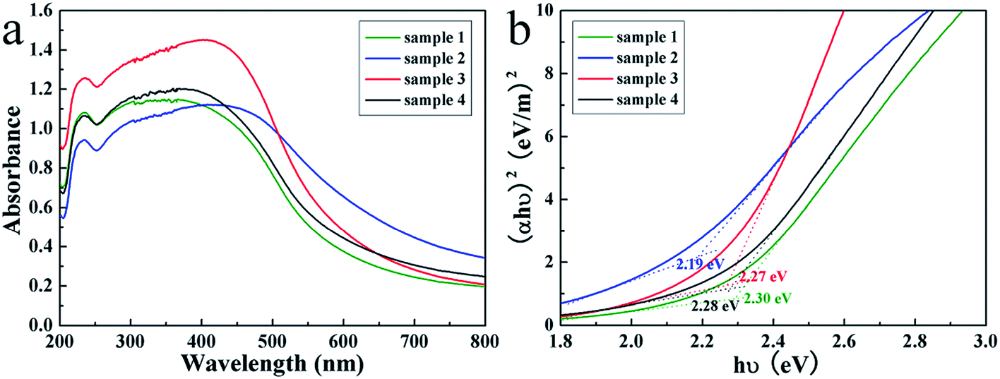 | ||
| Fig. 5 The UV-visible diffuse reflectance spectra (a) and the Tauc plots (b) of the SnS2 nanosheet-based microstructures. | ||
The BET surface areas of the four samples were determined by the nitrogen sorption experiments. As shown in Fig. 6, the products all exhibit type IV isotherms with a hysteresis loop, and the BJH pore size distribution in the inset indicated the existence of mesopores, which can be ascribed to the aggregation of the primary SnS2 nanostructures. The value of the BET surface area was 22.91 m2 g−1 for sample 1, merely 9.79 m2 g−1 for sample 2, maximally 161.57 m2 g−1 for sample 3, and 70.06 m2 g−1 for sample 4. The sample 3 and 4 have larger BET surface areas compared to the sample 1 and 2, which may be attributed to the enlarged interspace among the assembled units of tiny nanosheets through adsorption of more diethylamine molecules. Moreover, the surface areas of 3D hierarchical nanostructures of sample 1 and 3 are more than two times than that of 2D nanostructures of corresponding sample 2 and 4, indicating 3D nanostructures can effectively depress the aggregation of nanounits. The SnS2 nanosheet-based architecture with larger surface area will be more beneficial for the adsorption and photocatalytic degradation of pollutants in water.
 | ||
| Fig. 6 Nitrogen adsorption–desorption isotherms of the SnS2 nanosheet-based microstructures. (a) sample 1, (b) sample 2, (c) sample 3, (d) sample 4. | ||
Evaluation of adsorptive and photocatalytic activities
The present SnS2 nanosheet-based microstructures were used as the adsorptive photocatalysts for photodegradation of organic pollutants, which are evaluated in the dark and then under visible light irradiation using different organic pollutants as probe molecules in aqueous solutions. The relevant data for MB is presented in Fig. 7a. The adsorption–desorption equilibrium of MB on the catalyst surface was achieved almost in 1 h (Fig. S3a†), and the four samples all had high adsorption capacities for MB molecules, reaching 53.8% with sample 1, 57.9% with sample 2, 68.7% with sample 3, and 66.6% with sample 4. Although the BET surface area of sample 1 is much larger than that of sample 2, and sample 3 is much larger than sample 4, the adsorption capacity of sample 2 is inversely slightly higher than that of sample 1, while that of sample 3 is only slightly higher than that of sample 4. Therefore, the adsorption capacity of the sample is attributed not only to its surface area, but also to other reasons such as the exposed facet. The photocatalytic degradation of the dye was generally evaluated after its adsorption–desorption equilibrium on the catalyst surface. Thus, the photocatalytic degradation rate of MB in the presence of sample 1 reaches 54.3% after 1 h, while 76.0% with sample 2, 78.3% with sample 3, and 84.7% with sample 4. As a comparison, the relevant data in the absence of catalyst is also tested, which showed the decomposition of MB was about 14.6%, indicating that the photoinduced self-sensitized photolysis can be induced by photo-absorption of MB itself. But, the degradation rate was remarkably enhanced when the SnS2 product was added as a photocatalyst. After the adsorption and visible light photocatalytic degradation, the removal of MB from the solution reaches 78.9% with sample 1, 89.9% with sample 2, 92.8% with sample 3 and 94.9% with sample 4. Considering the amount of the catalyst and the dye used, the removal efficiencies of MB with as-prepared SnS2 nanosheet-based microstructures are high, especially with sample 3 and 4. | ||
| Fig. 7 Photocatalytic degradation curves of different organic pollutants aqueous solutions in the presence of as-prepared SnS2 nanosheet-based microstructures under visible light irradiation. (a) MB, (b) RhB, (c) MO, (d) phenol. | ||
The adsorptive and photocatalytic performances of the SnS2 products were also tested in another cationic dye of RhB solution. The adsorption capacities after 1 h for RhB molecules are 16.3% with sample 1, 20.2% with sample 2, 58.4% with sample 3, and 54.0% with sample 4 (Fig. S3b†). The photocatalytic degradation rate of RhB solution reaches 76.2% after 2 h with sample 1, while 76.8% with sample 2, 83.9% with sample 3, and 89.1% with sample 4 (Fig. 7b). Meanwhile, there was about 13.2% degradation in the absence of catalyst, indicating the photo-absorption of RhB molecules can also induce a small quantity of self-sensitized photolysis. The results showed there needed longer visible light irradiation time for effective photodegradation of RhB molecules than for MB molecules, revealing more energy was needed for the mineralization of RhB molecules. After the adsorption and visible light photocatalytic degradation, the total removal of RhB molecules from the solution reaches 80.1% with sample 1, 81.5% with sample 2, 93.3% with sample 3 and 95.0% with sample 4. The sample 3 and 4 showed superior photocatalytic activities than that of the sample 1 and 2, which is related with their higher specific surface areas and more exposed facets that enlarged the absorption capacity of reactant molecules as well as enhanced the visible light absorption.
As is known a prerequisite for efficient photodegradation pathway is the preadsorption of dye molecules on the photocatalyst surface in which excited dye molecules can inject electrons into the conduction band (CB) of the semiconductor.49–51 Consequently, the charge properties of photocatalyst surface and dye molecule are critical for the adsorption. To further clarify the adsorptive and photocatalytic processes, an anionic dye of MO was used as a probe molecule for comparison. The result showed the adsorption capacity was only 3.0% with sample 1, 2.6% with sample 2, 4.1% with sample 3 and 4.5% with sample 4 after 1 h in the dark (Fig. S3c†), demonstrating the anionic dye of MO is difficult to be adsorbed on the sample surface. Correspondingly, the photocatalytic degradation rate of MO molecules was 22.4% with sample 1, 14.2% with sample 2, 29.5% with sample 3, and 21.3% with sample 4 under visible light irradiation for 1 h (Fig. 7c), which is much lower than that of MB and RhB. At the same time, only 0.7% photodegradation was acquired without catalyst, indicating that the photoinduced self-sensitized photolysis can be ignored. The total removal of MO only reaches 24.7% with sample 1, 16.4% with sample 2, 32.4% with sample 3 and 24.8% with sample 4. The lower degradation rate of MO can be mainly attributed to the less adsorption on the photocatalyst since the photocatalytic process is commonly believed to occur on the photocatalyst surface. The adsorption capacities of anionic dye of MO on the surface of the SnS2 nanosheet-based microstructures are much lower than that of cationic dyes of MB and RhB, unveiling the photocatalyst surface is electronegative,5,25 which is probably come from the adsorption of diethylamine molecules during the synthetic process, where the N atom with a lone pair electrons favors the adsorption of positively charged dye molecules. Our work gives the clear investigation on the adsorption and photocatalytic degradation of different charged dye molecules with as-synthesized SnS2 nanosheet-based microstructures, which is helpful to disclose the adsorptive and photocatalytic processes more clearly.
To identify the dye photosensitization on enhancing the visible-light driven photodegradation of color organics, a comparative experiment of the photocatalytic degradation of colorless organics of phenol was carried out under visible light irradiation (Fig. 7d). There was only slightly adsorption and photodegradation within the test period. Therefore, it is reasonably believed that the indirect color dye photosensitization, i.e. dye degradation by the electron injection from dye to semiconductor plays a crucial role in the degradation of color dyes of MB, RhB and MO under visible light irradiation. The adsorption capacity, photocatalytic degradation and total removal of four different organics from the solution with the samples were listed in Table S2.†
The durability of the SnS2 nanosheet-based microstructures was tested with sample 4 by MB adsorption and photodegradation for five recycles, which was realized by recycling and washing the catalyst in dimethyl sulfoxide for two times. As shown in Fig. S4,† the catalyst can remove MB from the solution efficiently without significant deactivation after five times recycling, and the removal percentage maintained up to 86.6% even for the fifth cycle, indicating good circulating effect, which is very important for real application.
Generally, the photocatalytic activity of a semiconductor photocatalyst is mainly ascribed to its ability for adsorbing target pollutant, the photoabsorption ability in the available light energy region, and the separation and transporting rate of the photogenerated electrons and holes in the catalyst. Herein, the negatively charged surface of SnS2 nanosheet-based microstructures favored the adsorption of cationic dyes by electrostatic attraction. Meanwhile, the unique 2D nanosheet-based microstructures facilitated the light harvesting and interfacial electron–hole separation and transfer. The product owned larger specific surface area and more exposed facet may provide more reactive sites for the adsorption and transportation of dye molecules as well as the light harvesting, thus, enhancing the photocatalytic efficiency.
Conclusions
This work provides a convenient solution-phase route to generate SnS2 nanosheet-based microstructures with flower-like, nanosheet-like, nest-like and nanoplate-like morphologies by oriented attachment of tiny 2D nanosheets, which is based on a simple reaction of SnCl4·5H2O and C5H10NS2Na·3H2O in the solvent of ethylene glycol with or without addition of acetic acid. The SnS2 nanosheet-based microstructures were used as adsorptive photocatalysts in photocatalytic degradation of different organic pollutants. The negatively charged surface of as-prepared photocatalysts enhanced the adsorption of cationic dyes of MB and RhB molecules and facilitated the photosensitization process, consequently, improved photocatalytic degradation activity. Moreover, the products showed microstructure-dependent adsorptive and photocatalytic performances, in which the product with larger surface area and more exposed facet exhibits superior adsorption capacity and photocatalytic activity, even with a high dye loading. The results provide some new insights for in-depth understanding of charge-dependent adsorptive and photocatalytic performances, which open a new avenue for the design of the adsorptive photocatalyst with high adsorption capacity and photocatalytic activity by engineering the charge nature on the photocatalyst surface.Acknowledgements
This work was financially supported by the Natural Science Foundation of China (21201007).Notes and references
- L. L. Yuan, D. D. Huang, W. N. Guo, Q. X. Yang and J. Yu, Appl. Clay Sci., 2011, 53, 272–278 CrossRef CAS PubMed.
- P. Hareesh, K. B. Babitha and S. Shukla, J. Hazard. Mater., 2012, 229–230, 177–182 CrossRef CAS PubMed.
- Z. He, S. G. Yang, Y. M. Ju and C. Sun, J. Environ. Sci., 2009, 21, 268–272 CrossRef CAS.
- C. C. Chen, W. H. Ma and J. C. Zhao, Chem. Soc. Rev., 2010, 39, 4206–4219 RSC.
- Z. C. Wu, H. Wang, Y. J. Xue, B. E. Li and B. Y. Geng, J. Mater. Chem. A, 2014, 2, 17502–17510 CAS.
- P. Wang, D. Z. Li, J. Chen, X. Y. Zhang, J. J. Xian, X. Yang, X. Z. Zheng, X. F. Li and Y. Shao, Appl. Catal., B, 2014, 160–161, 217–226 CrossRef CAS PubMed.
- S. Khanchandani, S. Kundu, A. Patra and A. K. Ganguli, J. Phys. Chem. C, 2013, 117, 5558–5567 CAS.
- S. Khanchandani, P. K. Srivastava, S. Kumar, S. Ghosh and A. K. Ganguli, Inorg. Chem., 2014, 53, 8902–8912 CrossRef CAS PubMed.
- Y. L. Liao, H. W. Zhang, Z. Y. Zhong, L. J. Jia, F. M. Bai, J. Li, P. Zhong, H. Chen and J. Zhang, ACS Appl. Mater. Interfaces, 2013, 5, 11022–11028 CAS.
- W. Chen, N. Zhang, M. Y. Zhang, X. T. Zhang, H. Gao and J. Wen, CrystEngComm, 2014, 16, 1201–1206 RSC.
- X. W. Zou, H. Q. Fan, Y. M. Tian and S. J. Yan, CrystEngComm, 2014, 16, 1149–1156 RSC.
- S. W. Verbruggen, M. Keulemans, M. Filippousi, D. Flahaut, G. V. Tendeloo, S. Lacombe, J. A. Martens and S. Lenaerts, Appl. Catal., B, 2014, 156–157, 116–121 CrossRef CAS PubMed.
- D. W. Ding, K. Liu, S. N. He, C. B. Gao and Y. D. Yin, Nano Lett., 2014, 14, 6731–6736 CrossRef CAS PubMed.
- S. A. Ansari, M. M. Khan, M. O. Ansari, J. Lee and M. H. Cho, J. Phys. Chem. C, 2013, 117, 27023–27030 CAS.
- C. Y. Su, L. Liu, M. Y. Zhang, Y. Zhang and C. L. Shao, CrystEngComm, 2012, 14, 3989–3999 RSC.
- Z. F. Jiang, J. J. Zhu, D. Liu, W. Wei, J. M. Xie and M. Chen, CrystEngComm, 2014, 16, 2384–2394 RSC.
- J. Li, J. Yan, C. Z. Liu, L. H. Dong, H. Lv, W. D. Sun and S. X. Xing, CrystEngComm, 2014, 16, 10943–10948 RSC.
- J. C. Sin, S. M. Lam, I. Satoshi, K. T. Lee and A. R. Mohamed, Appl. Catal., B, 2014, 148–149, 258–268 CrossRef CAS PubMed.
- A. Kumar and T. Mohanty, J. Phys. Chem. C, 2014, 118, 7130–7138 CAS.
- V. Likodimos, C. Han, M. Pelaez, A. G. Kontos, G. L. Liu, D. W. Zhu, S. J. Liao, A. A. de la Cruz, K. O'Shea, P. S. M. Dunlop, J. A. Byrne, D. D. Dionysiou and P. Falaras, Ind. Eng. Chem. Res., 2013, 52, 13957–13964 CrossRef CAS.
- X. Y. Wu, S. Yin, Q. Dong, C. S. Guo, T. Kimura, J. I. Matsushita and T. Sato, J. Phys. Chem. C, 2013, 117, 8345–8352 CAS.
- L. G. Gai, X. Q. Duan, H. H. Jiang, Q. H. Mei, G. W. Zhou, Y. Tian and H. Liu, CrystEngComm, 2012, 14, 7662–7671 RSC.
- M. C. Wu, J. S. Chih and W. K. Huang, CrystEngComm, 2014, 16, 10692–10699 RSC.
- M. Zhang, J. Xu, R. L. Zong and Y. F. Zhu, Appl. Catal., B, 2014, 147, 229–235 CrossRef CAS PubMed.
- M. L. Guan, C. Xiao, J. Zhang, S. J. Fan, R. An, Q. M. Cheng, J. F. Xie, M. Zhou, B. J. Ye and Y. Xie, J. Am. Chem. Soc., 2013, 135, 10411–10417 CrossRef CAS PubMed.
- H. F. Cheng, B. B. Huang, Z. Y. Wang, X. Y. Qin, X. Y. Zhang and Y. Dai, Chem.–Eur. J., 2011, 17, 8039–8043 CrossRef CAS PubMed.
- X. Li, J. Zhu and H. X. Li, Appl. Catal., B, 2012, 123–124, 174–181 CrossRef CAS PubMed.
- W. M. Du, D. H. Deng, Z. T. Han, W. Xiao, C. Bian and X. F. Qian, CrystEngComm, 2011, 13, 2071–2076 RSC.
- J. F. Chao, Z. Xie, X. B. Duan, Y. Dong, Z. R. Wang, J. Xu, B. Liang, B. Shan, J. H. Ye, D. Chen and G. Z. Shen, CrystEngComm, 2012, 14, 3163–3168 RSC.
- Y. Q. Lei, S. Y. Song, W. Q. Fan, Y. Xing and H. J. Zhang, J. Phys. Chem. C, 2009, 113, 1280–1285 CAS.
- H. X. Zhong, G. Z. Yang, H. W. Song, Q. Y. Liao, H. Cui, P. K. Shen and C. X. Wang, J. Phys. Chem. C, 2012, 116, 9319–9326 CAS.
- J. Y. Chen, G. Y. Li, Z. G. He and T. C. An, J. Hazard. Mater., 2011, 190, 416–423 CrossRef CAS PubMed.
- Y. Z. Li and S. J. Kim, J. Phys. Chem. B, 2005, 109, 12309–12315 CrossRef CAS PubMed.
- J. G. McEvoy and Z. S. Zhang, Appl. Catal., B, 2014, 160–161, 267–278 CrossRef PubMed.
- S. S. Ma, J. J. Xue, Y. M. Zhou, Z. W. Zhang and X. Wu, CrystEngComm, 2014, 16, 4478–4484 RSC.
- J. W. Seo, Y. W. Jun, S. W. Park, H. Nah, T. Moon, B. Park, J. G. Kim, Y. J. Kim and J. Cheon, Angew. Chem., Int. Ed., 2007, 46, 8828–8831 CrossRef CAS PubMed.
- P. Chen, Y. Su, H. Liu and Y. Wang, J. Hazard. Mater., 2013, 5, 12073–12082 CAS.
- Y. C. Zhang, Z. N. Du, S. Y. Li and M. Zhang, Appl. Catal., B, 2010, 95, 153–159 CrossRef CAS PubMed.
- H. J. Chang, E. J. In, K. J. Kong, J. O. Lee, Y. M. Choi and B. H. Ryu, J. Phys. Chem. B, 2005, 109, 30–32 CrossRef CAS PubMed.
- Y. C. Zhang, Z. N. Du, K. W. Li, M. Zhang and D. D. Dionysiou, ACS Appl. Mater. Interfaces, 2011, 3, 1528–1537 CAS.
- Y. C. Zhang, J. Li, M. Zhang and D. D. Dionysiou, Environ. Sci. Technol., 2011, 45, 9324–9331 CrossRef CAS PubMed.
- W. D. Shi, L. H. Huo, H. S. Wang, H. J. Zhang, J. H. Yang and P. H. Wei, Nanotechnology, 2006, 17, 2918–2924 CrossRef CAS.
- J. Xia, G. C. Li, Y. C. Mao, Y. Y. Li, P. K. Shen and L. P. Chen, CrystEngComm, 2012, 14, 4279–4283 RSC.
- J. M. Ma, D. N. Lei, L. Mei, X. C. Duan, Q. H. Li, T. H. Wang and W. J. Zheng, CrystEngComm, 2012, 14, 832–836 RSC.
- C. X. Zhai, N. Du, H. Zhang and D. R. Yang, Chem. Commun., 2011, 47, 1270–1272 RSC.
- Y. F. Sun, H. Cheng, S. Gao, Z. H. Sun, Q. H. Liu, Q. Liu, F. C. Lei, T. Yao, J. F. He, S. Q. Wei and Y. Xie, Angew. Chem., Int. Ed., 2012, 51, 8727–8731 CrossRef CAS PubMed.
- H. Kaneka, S. Nishimoto, K. Miyake and N. Suedomi, J. Appl. Phys., 1986, 59, 2526–2534 CrossRef PubMed.
- S. J. Hong, S. Lee, J. S. Jang and J. S. Lee, Energy Environ. Sci., 2011, 4, 1781–1787 CAS.
- L. Q. Ye, L. Zan, L. H. Tian, T. Y. Peng and J. J. Zhang, Chem. Commun., 2011, 47, 6951–6953 RSC.
- J. C. Zhao, T. X. Wu, K. Q. Wu, K. Oikawa, H. Hidaka and N. Serpone, Environ. Sci. Technol., 1998, 32, 2394–2400 CrossRef CAS.
- T. X. Wu, G. M. Liu, J. C. Zhao, H. Hidaka and N. Serpone, J. Phys. Chem. B, 1998, 102, 5845–5851 CrossRef CAS.
Footnote |
| † Electronic supplementary information (ESI) available. See DOI: 10.1039/c5ra00395d |
| This journal is © The Royal Society of Chemistry 2015 |