DOI:
10.1039/C4RA07528E
(Paper)
RSC Adv., 2014,
4, 49228-49235
SiC nanocrystals: high-rate deposition and nano-scale control by thermal plasma
Received
24th July 2014
, Accepted 10th September 2014
First published on 11th September 2014
Abstract
This work used thermal plasma to enhance the deposition process of SiC nanocrystals, with SiCl4 and CH4 as the Si source and C source, respectively. Thin films containing SiC nanocrystals, a-Si and graphite were deposited on the substrates. The morphology and crystalline structure of the samples were characterized by various techniques, including SEM, TEM, and XRD. SiC nanocrystals were observed being covered by carbon films and embedded in the network formed by graphite and a-Si. The effect of SiCl4 input rate on the deposition process and product properties was studied in detail, combining characterization techniques and optical emission spectroscopy (OES) diagnostic results. Based on the OES diagnostic of the plasma zone, the concentrations of atomic Si and C in the gas phase are concluded to be the main factors affecting the deposition process. Finally, a simple deposition mechanism is deduced based on the experimental results, which indicates the formation of SiC nanocrystals through the assembly of atomic species in the plasma.
1. Introduction
Silicon carbide (SiC) is a well-known wide-bandgap semiconductor with excellent thermal, mechanical and electrical properties, such as high thermal conductivity, high resistance to shocks, high breakdown voltage, high electron saturation velocity and chemical inertness.1,2 It has been the material of choice for high-voltage and high-current devices operating at elevated temperatures.3,4 It is also biocompatible with blood and can be utilized as the coating material of artificial joints.5 Large-area, high-quality, single-crystal SiC substrates are nowadays available due to advances in crystallization techniques. In recent years, the discovery of new forms of SiC, such as superlattices and nanocrystals, has been triggered by nanotechnology. SiC nanocrystals have several superior properties in comparison with bulk SiC materials. Among them, the photoluminescence (PL) properties of SiC nanocrystals have been paid close attention and been widely studied.6–10 The biocompatibility of SiC nanocrystals has allowed them to be applied in in vivo biological imaging as biomarkers, which requires the production of SiC nanocrystals in relatively large amounts.11–14
SiC nanocrystals are conventionally produced by chemical etching or plasma-enhanced chemical vapor deposition (PECVD). Fabrication of SiC nanocrystals using electrochemical anodization has been reported since the 1990s.6,7,15 This method, however, involves corrosive solutions and the fabrication process is relatively slow, which makes it difficult to produce these nanocrystals at the industrial scale. Wet chemical etching has replaced the electrochemical anodization method to become the major method for SiC nanocrystal fabrication.9,10,16,17 Nanocrystals prepared by wet chemical etching have advantageous features such as small diameters and a narrow size distribution. Moreover, the wet chemical etching process is simple and can be easily conducted in the laboratory. However, this process also involves corrosive solutions, which may lead to sewage pollution when applied on a large scale. PECVD is a cleaner process and is widely applied for the synthesis of nanomaterials.18–20 Moreover, PECVD is the most commonly used technique for the production of cubic SiC (3C-SiC and β-SiC), and has also been applied for SiC nanocrystal fabrication during the past decade.21–28 SiH4 and hydrocarbons have generally been used as silicon and carbon source gases, respectively,21–23 while organosilane has been used as a single source for both Si and C.27 Both radio-frequency (RF) plasma21,22 and electron cyclotron resonance (ECR) plasma23 could be adopted in PECVD processes. Moreover, SiC nanocrystals can also be deposited by reactive plasma sputtering of bulk Si and C or SiC targets.24–26,28 However, these cold plasma-enhanced CVD processes all have low deposition rates, which makes it difficult to fabricate SiC nanocrystals on a large scale and thus hampers the industrial applications of SiC nanocrystals.
Thermal plasma enhancement has been adopted in high-rate CVD of nanocrystalline silicon (nc-Si) to obtain a deposition rate of 9.78 nm s−1.29 Compared to cold plasma, thermal plasma offers higher temperature and higher reactive species density, and thus offers much higher fluxes of energy and matter in nanomaterial fabrication.30,31 Chaudhry et al.22 has utilized a 15 kW source of thermal plasma to fabricate polycrystalline SiC and studied the influence of deposition temperature. However, there are few reported analyses of the thermal plasma deposition process and product properties. In this work, SiC nanocrystals were fabricated using an atmospheric-pressure thermal-plasma-enhanced CVD (APTPECVD) process and the effects of raw material input rate on the deposition process and product properties were studied. Inductively coupled plasma (ICP) was adopted, which is particularly appropriate for high-purity product synthesis owing to the absence of an electrode.
We chose SiCl4 instead of SiH4 or organosilane as the Si source. SiH4 is a hazardous material because of its pyrophoricity in air,32 while SiCl4 is chemically more stable, and is a liquid at room temperature. Most SiCl4 is made in the photovoltaics industry as a by-product of polycrystalline silicon fabrication using the SIMENS method. About 10–15 t high-purity SiCl4 is produced when producing 1 t of polycrystalline silicon. The resulting large supply of SiCl4 has in turn led to its price being much lower than that of most organosilanes, and this makes SiCl4 more appropriate than either organosilanes or SiH4 as a source of Si for thermal plasma processes.
To the best of our knowledge, this is the first time that the use of SiCl4 as a Si source for SiC nanocrystal fabrication through a PECVD process has been reported. Furthermore, an optical emission spectroscopy (OES) diagnostic was carried out during the thermal-plasma-enhanced CVD process to analyze the gas phase composition in the plasma zone and better understand the plasma deposition process.33
2. Results and discussion
Samples were deposited on both crystalline silicon (c-Si) and glass substrates. X-ray diffraction (XRD) patterns of samples at different SiCl4 input rates are shown in Fig. 1. Diffraction peaks at 35.414°, 41.231°, 59.879° and 71.610° correspond to the (111), (200), (220) and (311) crystal planes of β-SiC. Broadened peaks at 25.782° and 68.545° correspond to the (002) plane of graphite and the (400) plane of c-Si, respectively. Silicon is in an amorphous phase according to the diffraction peak structure observed. Therefore, SiC nanocrystals are embedded in a mixture of graphite and a-Si. A diffraction peak at 29.396°, which corresponds to the (111) plane of c-Si, was observed at a very low SiCl4 input rate, i.e., 0.11 mol h−1, while the intensities of the diffraction peaks of β-SiC are relatively low. So the sample is mainly composed of a-Si and graphite at very low SiCl4 input rates. However, the intensities of the diffraction peaks from the (111), (220) and (311) crystal planes of SiC were observed to increase with an increase of SiCl4 input rate. The diffraction peak of the (200) crystal plane of SiC became noticeable when the SiCl4 input rate exceeded 0.32 mol h−1. The broadening of the diffraction peaks is due to the anisotropic shape of the crystallites, while the relatively large width of the peaks indicates the presence of very small SiC grain diameters.28 The average diameters of SiC grain at different SiCl4 input rates were calculated using Scherrer's formula:| |
 | (1) |
where λ is the X-ray beam wavelength (λ = 1.54056 Å in this work) and β is the broadening of the X-ray diffraction line expressed in radians.34 The average grain diameters were calculated to be in the range of 21–33 nm and are summarized in Table 1.
 |
| | Fig. 1 XRD patterns of samples deposited at different SiCl4 input rates. | |
Table 1 SiC grain diameters of samples at different SiCl4 input rates, calculated using Scherrer's formula
| SiCl4 input rate (mol h−1) |
Grain diameter (nm) |
| 0.11 |
33 |
| 0.21 |
24 |
| 0.32 |
24 |
| 0.42 |
29 |
| 0.53 |
32 |
| 0.63 |
21 |
The results of Raman spectrum analysis agree well with XRD characterization. The typical Raman spectrum of the sample deposited at a SiCl4 input rate of 0.53 mol h−1 is given in Fig. 2(a). The broad peak centered on 480 cm−1 originates from a-Si.35 The peaks at ∼1350 cm−1, ∼1580 cm−1 and ∼2690 cm−1 correspond to the D band, G band and 2D band of graphite, respectively.36,37 The intensities of the D band and 2D band peaks are relatively high, which indicates the existence of defects in the graphite structure.38 Based on analysis of the XRD and Raman spectra, the thin film appears to be composed of SiC nanocrystals, a-Si and graphite. The intensities of the D band and the G band both decreased with increasing SiCl4 input rate, as shown in Fig. 2(b). This may result from the decrease of the amount of graphite in the product with increasing SiCl4 input rate. The intensity ratio of the D band to G band increased with increasing SiCl4 input rate, which means that the amount of disordered structures in graphite increases with increasing SiCl4 input rate.36 The effect of SiCl4 input rate on product composition and properties will be further analyzed and discussed later.
 |
| | Fig. 2 (a) Typical Raman spectrum of a sample at a SiCl4 input rate of 0.53 mol h−1; (b) effect of SiCl4 input rate on the intensities of the D band and G band, and on the intensity ratio of the D band to the G band. | |
The samples have porous structures as shown in the scanning electron microscope (SEM) images in Fig. 3. This porous structure consists of nano-sized spheres and branched networks. All samples were observed to have similar network structures, but with the diameters of the spheres changing with SiCl4 input rate. Film thickness was determined from the cross-sectional SEM images of the samples, as shown in Fig. 3(e), and was used to calculate the deposition rates of the thin films. The effect of SiCl4 input rate on deposition rate is given in Fig. 4. The deposition rate increased with increasing SiCl4 input rate. This deposition rate with thermal plasma enhancement reached a maximum of ∼70 nm s−1, which is relatively high compared with that of cold plasma processes.19
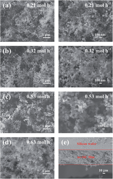 |
| | Fig. 3 SEM images of samples at SiCl4 input rates of (a) 0.21 mol h−1, (b) 0.32 mol h−1, (c) 0.53 mol h−1 and (d) 0.63 mol h−1; (e) a typical cross-sectional SEM image of the sample at a SiCl4 input rate of 0.42 mol h−1. | |
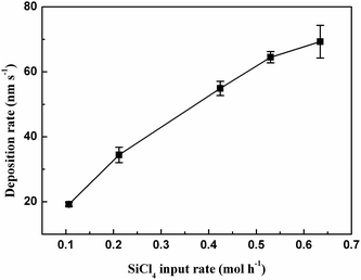 |
| | Fig. 4 Effect of SiCl4 input rate on thin-film deposition rate. | |
Transmission electron microscopy (TEM) was carried out to further investigate the morphology of the samples. Fig. 5 shows the typical TEM images of samples at different SiCl4 input rates. SiC nanocrystals and graphite, as indicated by XRD and Raman spectra analysis, are observed and marked in the images. SiC nanocrystals are formed covered with a carbon film and embedded in a network consisting of a-Si and graphite. The diameters of the SiC nanocrystals were measured to be in the range from less than 10 nm to larger than 30 nm. The carbon film covering the SiC nanocrystal consists of 2–5 layers of graphene. Clear lattice fringes were observed during the TEM analysis. The lattice fringe spacing of SiC grain was determined from the images to be 2.5 Å, corresponding to the (111) crystal plane of β-SiC, which agrees well with the fast Fourier transformation (FFT) results shown in Fig. 5. Only the (111) crystal plane of β-SiC is observed in the FFT images, which means that (111) is the preferential crystal orientation, as also shown by the XRD results. Meanwhile, the lattice fringe of the (002) crystal plane of graphite can be also identified, and was determined to be 3.4 Å. The (002) crystal plane of graphite was identified to be the preferential crystal orientation in the FFT image of the graphite phase, which agrees well with the XRD results. A curve and fracture in the graphite phase, which leads to the high intensity of the D band in the Raman analysis, was observed in the TEM images.
 |
| | Fig. 5 Typical bright-field TEM images with associated FFT patterns of samples at SiCl4 input rates of (a and b) 0.42 mol h−1; (c) 0.53 mol h−1. | |
The chemical compositions of surfaces of the samples were analyzed by X-ray photoelectron spectroscopy (XPS). The surface of the sample consists of Si, C, O, and Cl, as indicated by the survey XPS spectrum in Fig. 6(a). The distinct peaks at around 101.82 eV, 284.80 eV, 532.59 eV, and 200.42 eV correspond to Si 2p, C 1s, O 1s, and Cl 2p, respectively. The chemical states of the surface elements were further analyzed by high-resolution XPS spectra. Moreover, the deconvolution of the spectra of Si 2p and C 1s was carried out. The Si 2p spectrum can be fitted into 3 peaks at 101.33 eV, 101.75 eV, and 103.07 eV, corresponding to Si from SiC,39 Si from SiO2,40 and Si from (–Si(CH3)2O–)n,41 respectively. The C 1s spectrum can also be fitted into peaks at 287.42 eV, 287.82 eV, and 285.92 eV, corresponding to C from SiC,42 C from graphite,43 and C from the carbon network, respectively.44 O comes from the oxidation of the sample surface. During thermal plasma deposition, dangling bonds such as those in Si–Cl, Si–H, and Si–CH3 were formed on the surface. These active bonds can be easily oxidized when coming into contact with air, leading to the formation of Si–O on the surface. Cl comes from remaining dangling bonds on the surface.
 |
| | Fig. 6 (a) Survey XPS spectrum of sample deposited at a SiCl4 input rate of 0.21 mol h−1 and spectra of (b) Si 2p and (c) C 1s. | |
The C atomic fraction of the samples, defined as the relative atomic fraction of C divided by the combined fraction of Si and C, was computed based on the analysis of the survey XPS spectrum. These results are summarized in Fig. 7(a). The C atomic fraction of the samples was determined to decrease with increasing SiCl4 input rate. Moreover, the mole fraction of SiC, defined as the relative mole concentration of Si from SiC divided by the combined mole concentration of Si from SiC, (–Si(CH3)2O–)n and SiO2, was calculated from the analysis of the XPS spectrum of Si 2p. The SiC mole fraction first increased and then decreased with increasing SiCl4 input rate, which can be seen in Fig. 7(b). The SiC mole fraction reached a maximum at a SiCl4 input rate of 0.21 mol h−1, which means that the most SiC components were obtained under this condition.
 |
| | Fig. 7 Effect of SiCl4 input rate on (a) C atomic fraction and (b) SiC mole fraction of samples. | |
To better understand the effect of SiCl4 input rate on the deposition process and product properties, an OES diagnostic of the thermal-plasma-enhanced deposition was carried out. A typical optical emission spectrum of the thermal plasma deposition at a SiCl4 input rate of 0.42 mol h−1 is shown in Fig. 8. Excited species such as Si*, C*, H*, and Ar* are observed and marked in the images, which indicates that thermal plasma has sufficient ability to decompose SiCl4, CH4, and H2 into atomic states. We studied the effect of SiCl4 input rate on the emission lines located at 288.17 nm, 247.83 nm, and 656.24 nm, which correspond to Si*, C*, and H*, respectively. As can be seen in Fig. 9, the emission intensity of Si (288.17 nm) was observed to increase with increasing SiCl4 input rate and then to plateau after the SiCl4 input rate reached 0.42 mol h−1.
 |
| | Fig. 8 Typical optical emission spectrum of thermal plasma deposition at a SiCl4 input rate of 0.42 mol h−1 and at wavelengths of (a) 200–500 nm and (b) 600–1000 nm. | |
 |
| | Fig. 9 Effect of SiCl4 input rate on the emission intensities of Si (288.17 nm), C (247.83 nm), and H (656.24 nm). | |
In this thermal plasma deposition system, the effect of precursors input on the electron density of the plasma can be negligible and thus the emission intensities of Si* and C* linearly correlate with the concentrations of atomic Si and C in the gas phase, respectively.33 Therefore, the increase of SiCl4 input rate enhanced the concentration of atomic Si in the gas phase while the concentration of atomic C first increased and then decreased, depending on the OES diagnostic results shown in Fig. 9. The concentrations of atomic Si and C in the gas phase were found to be the main factors affecting the deposition process and product properties. Higher atomic Si concentrations in the gas phase led to more Si being deposited in the sample, resulting in the increase of thin-film deposition rate and the decrease of C atomic fraction. More SiC formed with more atomic Si and C in the gas phase when the SiCl4 input rate first increased. However, the amount of atomic C then turned out to be insufficient and the redundant Si prefers to form a-Si rather than SiC, which led to the decrease of SiC mole fraction at higher SiCl4 input rates.
Based on the characterization and OES diagnostic results summarized above, the deposition mechanism in the APTPECVD process was simply deduced and is shown in Fig. 10. Si source (SiCl4) and C source (CH4) together with H2 are imported into the thermal plasma, where these precursors are decomposed into atomic Si, C, H, and Cl through eqn (2)–(4) (with M representing e− or Ar).
| | |
SiCl4 + M → Si + 4Cl + M,
| (2) |
| | |
CH4 + M → C + 4H + M,
| (3) |
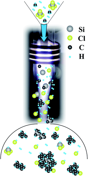 |
| | Fig. 10 Schematic diagram of the deposition mechanism of the APTPECVD process. | |
When these excited species flow to a low-temperature zone, they begin to combine, leading to the formation of small molecules, such as HCl and chlorosilanes, and crystal nuclei through eqn (5)–(8).
| | |
Si + xH + (4 − x)Cl → SiHxCl4−x, (x = 0, 1, 2, 3)
| (6) |
Collisions cause the crystal nuclei to grow as they continue to travel in the plasma to locations with lower temperatures. As the input rate of CH4 is higher than that of SiCl4, more C-related species are formed in the plasma. C is found not only in SiC but also in graphite. Small molecules and clusters prefer to attach themselves onto particles previously formed in the plasma, such as SiC nanocrystals. Finally, these particles leave the plasma and get deposited on the substrate to form thin-film samples. This process results in the morphology observed in Fig. 5 – i.e., SiC nanocrystals covered by carbon films and embedded in the network formed by graphite and a-Si – and explains the appearance of dangling bonds on the surface of the sample.
3. Experimental
3.1 Fabrication of SiC nanocrystals
The APTPECVD apparatus with OES diagnostic equipment has been described elsewhere.29,33 The thermal plasma was generated by an RF plasma source with power up to 10 kW. SiCl4 and CH4 diluted by H2 were used as Si and C sources, respectively. Ar was the plasma working gas. The input rate of SiCl4 was tested from 0.11 to 0.63 mol h−1 to determine the effect of SiCl4 input rate on the deposition process while the input rates of CH4 and H2 were fixed at 0.51 and 1.54 mol h−1. The volatile SiCl4 precursor was transferred into a plastic injector in a fuming cupboard and pumped into the deposition system using an injection pump. Both crystalline silicon and glass were used as substrates.
3.2 Characterization
The morphology and nanostructure of the samples were characterized using a scanning electron microscope (SEM, JSM-6460LV) and a transmission electron microscope (HRTEM, JEM-2010). The crystal structure of the sample was analyzed by X-ray diffraction (Bruker D8 Advance) with monochromatized Cu Kα radiation between scattering angles of 5° and 90° and a micro Raman spectroscope (Horibra LABRAM-HR) with 532 nm He–Ne laser excitation between wavelengths of 300 and 3000 cm−1. The elemental composition of the sample surface was analyzed by X-ray photoelectron spectroscopy (ESCALAB 250Xi) with Al Kα radiation, and the C 1s peak at 284.6 eV was used as an internal standard.
4. Conclusion
The SiC nanocrystal is a promising material with potential applications in electronics, photovoltaics and biological fields. In this work, SiC nanocrystals were fabricated using an APTPECVD process with SiCl4 as the Si source and CH4 as the C source. The thermal-plasma-enhanced CVD process and product properties were thoroughly studied. The SiC nanocrystals produced were covered by carbon films and embedded in the network formed by graphite and a-Si. The deposition rate of the thin film increased with increasing SiCl4 input rate and reached a maximum of ∼70 nm s−1. The SiC nanocrystal has an average grain diameter in the range of 21–33 nm. The effect of SiCl4 input rate on the surface chemical compositions of the samples was studied, and the C atomic fraction and SiC mole fraction of the samples were calculated. An OES diagnostic was carried out to better understand the effect of SiCl4 input rate on the deposition process. The concentrations of atomic Si and C in the gas phase were found to be the main factors affecting deposition rate and product properties. Based on these experimental results, a simple deposition mechanism in the APTPECVD process was deduced, indicating that SiC nanocrystals were formed by the assembly of atomic species formed by thermal plasma decomposition of Si and C precursors.
Acknowledgements
This study was supported by the National Basic Research Program of China (973 Program no. 2012CB720301), the National Natural Science Foundation of China (NSFC) under grant no. 21176137. We are also grateful for Mr Zezhong Cao's help on the deposition experiments.
References
- D. Nakamura, I. Gunjishima, S. Yamaguchi, T. Ito, A. Okamoto, H. Kondo, S. Onda and K. Takatori, Nature, 2004, 430, 1009–1012 CrossRef CAS PubMed.
- P. Melinon, B. Masenelli, F. Tournus and A. Perez, Nat. Mater., 2007, 6, 479–490 CrossRef CAS PubMed.
- C. R. Eddy and D. K. Gaskill, Science, 2009, 324, 1398–1400 CrossRef CAS PubMed.
- S. Castelletto, B. C. Johnson, V. Ivady, N. Stavrias, T. Umeda, A. Gali and T. Ohshima, Nat. Mater., 2014, 13, 151–156 CrossRef CAS PubMed.
- P. Aspenberg, A. Anttila, Y. T. Konttinen, R. Lappalainen, S. B. Goodman, L. Nordsletten and S. Santavirta, Biomaterials, 1996, 17, 807–812 CrossRef CAS.
- T. Matsumoto, J. Takahashi, T. Tamaki, T. Futagi, H. Mimura and Y. Kanemitsu, Appl. Phys. Lett., 1994, 64, 226–228 CrossRef CAS PubMed.
- J. S. Shor, L. Bemis, A. D. Kurtz, I. Grimberg, B. Z. Weiss, M. F. Macmillian and W. J. Choyke, J. Appl. Phys., 1994, 76, 4045–4049 CrossRef CAS PubMed.
- Y. P. Guo, J. C. Zheng, A. Wee, C. Huan, K. Li, J. S. Pan, Z. C. Feng and S. J. Chua, Chem. Phys. Lett., 2001, 339, 319–322 CrossRef CAS.
- J. Zhu, Z. Liu, X. L. Wu, L. L. Xu, W. C. Zhang and P. K. Chu, Nanotechnology, 2007, 18, 36560336 Search PubMed.
- D. J. Dai, N. Zhang, W. X. Zhang and J. Y. Fan, Nanoscale, 2012, 4, 3044–3046 RSC.
- J. Y. Fan, H. X. Li, J. Iiang, L. So, Y. W. Lam and P. K. Chu, Small, 2008, 4, 1058–1062 CrossRef CAS PubMed.
- J. Y. Fan and P. K. Chu, Small, 2010, 6, 2080–2098 CrossRef CAS PubMed.
- B. Somogyi, V. Zolyomi and A. Gali, Nanoscale, 2012, 4, 7720–7726 RSC.
- D. Beke, Z. Szekrenyes, D. Palfi, G. Rona, I. Balogh, P. A. Maak, G. Katona, Z. Czigany, K. Kamaras, B. Rozsa, L. Buday, B. Vertessy and A. Gali, J. Mater. Res., 2013, 28, 205–209 CrossRef CAS.
- J. S. Shor, I. Grimberg, B. Z. Weiss and A. D. Kurtz, Appl. Phys. Lett., 1993, 62, 2836–2838 CrossRef CAS PubMed.
- D. Beke, Z. Szekrenyes, I. Balogh, M. Veres, E. Fazakas, L. K. Varga, K. Kamaras, Z. Czigany and A. Gali, Appl. Phys. Lett., 2011, 99, 21310821 CrossRef PubMed.
- Y. Li, C. X. Chen, J. T. Li, Y. Yang and Z. M. Lin, Nanoscale Res. Lett., 2011, 6, 454 CrossRef PubMed.
- S. Askari, I. Levchenko, K. Ostrikov, P. Maguire and D. Mariotti, Appl. Phys. Lett., 2014, 104, 163103–163105 CrossRef PubMed.
- Q. Cheng, E. Tam, S. Xu and K. K. Ostrikov, Nanoscale, 2010, 2, 594–600 RSC.
- K. K. Ostrikov, D. H. Seo, H. Mehdipour, Q. Cheng and S. Kumar, Nanoscale, 2012, 4, 1497–1508 RSC.
- T. Takeshita, K. Ichige, Y. Kurata and S. Hasegawa, J. Appl. Phys., 1991, 69, 7945–7947 CrossRef CAS PubMed.
- M. I. Chaudhry and R. L. Wright, Appl. Phys. Lett., 1991, 59, 51–53 CrossRef CAS PubMed.
- K. L. Cheng, H. C. Cheng, W. H. Lee, C. P. Lee, C. C. Liu and T. R. Yew, Appl. Phys. Lett., 1997, 70, 223–225 CrossRef CAS PubMed.
- Y. Sun, T. Miyasato, J. K. Wigmore, N. Sonoda and Y. Watari, J. Appl. Phys., 1997, 82, 2334–2341 CrossRef CAS PubMed.
- S. Kerdiles, R. Rizk, A. Perez-Rodriguez, B. Garrido, O. Gonzalez-Varon, L. Calvo-Barrio and J. R. Morante, Solid-State Electron., 1998, 42, 2315–2320 CrossRef CAS.
- S. Kerdiles, A. Berthelot, F. Gourbilleau and R. Rizk, Appl. Phys. Lett., 2000, 76, 2373–2375 CrossRef CAS PubMed.
- T. Rajagopalan, X. Wang, B. Lahlouh, C. Ramkumar, P. Dutta and S. Gangopadhyay, J. Appl. Phys., 2003, 94, 5252–5260 CrossRef CAS PubMed.
- H. Colder, R. Rizk, M. Morales, P. Marie, J. Vicens and I. Vickridge, J. Appl. Phys., 2005, 98, 0243132 CrossRef PubMed.
- T. F. Cao, H. B. Zhang, B. H. Yan and Y. Cheng, RSC Adv., 2013, 3, 20157–20162 RSC.
- K. K. Ostrikov, U. Cvelbar and A. B. Murphy, J. Phys. D: Appl. Phys., 2011, 44, 17400117 Search PubMed.
- K. K. Ostrikov, E. C. Neyts and M. Meyyappan, Adv. Phys., 2013, 62, 113–224 CrossRef CAS.
- P. W. Atkins, T. L. Overton, J. P. Rourke, M. T. Weller and F. A. Armstrong, Inorganic Chemistry, W. H. Freeman and Company, New York, 5th edn, 2010 Search PubMed.
- T. F. Cao, H. B. Zhang, B. H. Yan, W. Lu and Y. Cheng, RSC Adv., 2014, 4, 15131–15137 RSC.
- H. Fritzsche, M. Tanielian, C. C. Tsai and P. J. Gaczi, J. Appl. Phys., 1979, 50, 3366–3369 CrossRef CAS PubMed.
- E. Bustarret, M. A. Hachicha and M. Brunel, Appl. Phys. Lett., 1988, 52, 1675–1677 CrossRef CAS PubMed.
- F. Tuinstra and J. L. Koenig, J. Chem. Phys., 1970, 53, 1126 CrossRef CAS PubMed.
- A. C. Ferrari, J. C. Meyer, V. Scardaci, C. Casiraghi, M. Lazzeri, F. Mauri, S. Piscanec, D. Jiang, K. S. Novoselov, S. Roth and A. K. Geim, Phys. Rev. Lett., 2006, 97, 18740118 Search PubMed.
- A. C. Ferrari and J. Robertson, Phys. Rev. B: Condens. Matter Mater. Phys., 2000, 61, 14095–14107 CrossRef CAS.
- T. M. Parrill and Y. W. Chung, Surf. Sci., 1991, 243, 96–112 CrossRef CAS.
- A. M. Venezia, R. Bertoncello and G. Deganello, Surf. Interface Anal., 1995, 23, 239–247 CrossRef CAS.
- M. Morra, E. Occhiello, R. Marola, F. Garbassi, P. Humphrey and D. Johnson, J. Colloid Interface Sci., 1990, 137, 11–24 CrossRef CAS.
- M. Johansson, A. J. Maxwell, S. M. Gray, P. A. Bruhwiler, D. C. Mancini, L. Johansson and N. Martensson, Phys. Rev. B: Condens. Matter Mater. Phys., 1996, 54, 13472–13475 CrossRef CAS.
- W. M. Lau, L. J. Huang, I. Bello, Y. M. Yiu and S. T. Lee, J. Appl. Phys., 1994, 75, 3385–3391 CrossRef CAS PubMed.
- Z. H. Wen, G. H. Lu, S. M. Cui, H. Kim, S. Q. Ci, J. W. Jiang, P. T. Hurley and J. H. Chen, Nanoscale, 2014, 6, 342–351 RSC.
|
| This journal is © The Royal Society of Chemistry 2014 |
Click here to see how this site uses Cookies. View our privacy policy here. 


