DOI:
10.1039/C4RA03430A
(Paper)
RSC Adv., 2014,
4, 32117-32126
An analytical approach for the energy spectrum and optical properties of gated bilayer graphene
Received
15th April 2014
, Accepted 11th June 2014
First published on 11th June 2014
Abstract
First, we present an analytical approach to access the exact energy spectrum and wave functions of gated Bernal bilayer graphene (BBLG), with all the tight-binding parameters included. To tackle the broken mirror symmetry caused by a gated voltage (Vg) and interlayer interactions, we create a unitary transformation to reduce the Hamiltonian matrix of BBLG to a simple form, which can offer the analytical energy spectrum. The formulae generate the gated tunable energy bands and reveal that Vg changes the subband spacing, produces the oscillating bands, and increases the band-edge states. Then, we employ the analytical model to revisit the optical dipole matrix element and optical absorption spectra. In the absence of Vg, the anisotropic dipole matrix element exhibits a maximum around the point M and zero value along the high symmetry line ΓK in the first Brillouin zone. Vg effectively induces the nonzero dipole matrix element along the high symmetry line ΓK, which makes a significant contribution in the absorption spectra. Moreover, the application of Vg opens an optical gap and gives rise to a profound low-energy peak in the absorption spectra. The dependence upon the gated bias Vg for the location and height of this peak clearly emerges through the analytical model. Our exact analytical model can be further used to study the many-body effect and exciton effect on the electronic and optical properties of BBLG.
1 Introduction
Graphene, a hit topic since 2004,1 having attracted a surge of interest for fundamental and experimental studies,2–9 is a one atom-thick layer made up of carbon atoms arranged in a honeycomb lattice. Stemming from the specular geometrical structure, graphene is an extraordinary two dimensional material with many unique properties, e.g., linear energy dispersions crossing at the Dirac point, electron–hole symmetry, Klein tunneling, high mobility at room temperature, and the novel quantum Hall effect.7–13 Its unusual electric properties make graphene a possible candidate for fabricating future electronic devices. Graphene is a zero band gap semiconductor due to linear energy dispersions crossing at the Dirac point. The presence of valence and conduction bands in its energy spectrum limits the on-off current ratios achievable and prevents the use of graphene in making field transistors. It is significant for the opening of a band gap in graphene to remove the limitation in using graphene material for semiconductor applications. Many breakthrough methods are proposed to generate a band gap in monolayer graphene, e.g., using molecular doping,14,15 the application of strain,16,17 and patterning a graphene sheet into a nanoribbon.18 On the other hand, a tunable band gap is induced in Bernal bilayer graphene (BBLG) through the application of a perpendicular electric field. BBLG is made up of two monolayer graphenes, held by weak Van der Waals forces in the AB-stacking. Experimental works demonstrate that a tunable band gap of up to 0.25 eV is achieved for electrically gated bilayer graphene by a variable external electric field.19–22
The energy dispersions of the gated BBLG are usually explored within the tight-binding model.23–31 The minimal model, considering only the intralayer and main interlayer interactions, is widely employed to study the energy dispersions of BBLG.30,31 Around the Dirac points, the analytical low-energy dispersions of gated BBLG are obtained through the continuum model. A 4 × 4 Hamiltonian matrix is solvable and gives out the analytical low-energy dispersions. A full tight-binding Hamiltonian model takes into account all hopping integrals, including the additional skew interaction (γ3) and electron–hole asymmetry (γ4) in the model.23,27 γ3 is the trigonal warping and γ4 is the origin of electron–hole asymmetry. The trigonal warping can significantly modify the physical properties of BBLG.32–34 Cserti has shown that trigonal warping has a great effect on the minimal conductivity of BBLG.32 Moreover, γ3 gives rise to the electron–hole asymmetry and distorts the circular equi-energy contour to a trigonal symmetry.33,34 A full tight-binding Hamiltonian matrix is a 4 × 4 matrix and its four energy bands are usually obtained by numerical diagonalization. Many important physical properties do not directly emerge through the numerical calculation because of a lack of the exact energy spectrum. To fully and exactly describe the electric and optical properties in the full energy region, an analytical description of the energy dispersions of the four-band model is expected.
Here, we present a model to access the analytical form of the energy spectrum and eigenstates of gated BBLG based on the tight-binding framework and all the tight-binding parameters, γ0, γ1, γ3 and γ4, are considered too (see the inset of Fig. 1(a)). Unlike AA-stacked grapheme,35,36 the skew interlayer interactions (γ3) and gated bias (Vg) destroy the inversion symmetry of gated BBLG. The broken symmetry increases the difficulty in solving the eigenvalue problem. Through a rotation operator, we generate a new set of tight-binding basis functions to deal with the broken symmetry resulting from the γ3 and Vg. The renormalized Vg-dependent intralayer and interlayer interactions are derived based on the new set of basis functions. Most importantly, the new basis functions exactly reduce the Hamiltonian matrix (H) into a band-storage matrix. As a result, the energy dispersions and wave functions are analytically solvable. Furthermore, the present work aims to provide full-frequency energy bands, which are beyond the effective mass approximation. The analytical form of the energy spectrum and eigenstates are further applied to study the optical absorption spectra and explore the origin of optical transition channels.
 |
| | Fig. 1 (a) The energy spectra, obtained using eqn (11), are illustrated by the red dashed curves. The black curves are the energy spectrum by numerical diagonalization. The geometric structure of the AB-stacked bilayer graphene and the intralayer and interlayer interactions are shown in the inset. (b) The same plots as in (a) but with the gated voltage Vg = 200 meV. The inset exhibits the first Brillouin zone. M is the saddle point and K and K′ are the Dirac points. | |
The rest of the paper is organized as follows: we develop a model to derive the analytical form of the energy spectrum of gated BBLG in Section 2. Subsequently, the electronic properties are revisited in Section 3 through the analytical energy spectrum. In Section 4, the energy spectrum and eigenstates are used to explore the dipole matrix element and optical absorption spectra of gated BBLG. Finally, the conclusions are drawn in Section 5.
2 Theory and model
BBLG is a stack of two identical graphene layers with a AB-stacking, as shown in the inset of Fig. 1(a). On each graphene plane, two basic atoms, A and B, are arranged in a honeycomb lattice and the bond length between atoms A and B is b = 1.42 Å. The distance between two graphene layers is assumed to be 3.35 Å.37 The lower or upper graphene layers are denoted by the index l = 1 or 2. Atoms A2 and A1 have the same (x, y) projection and they are denoted as the dimer sites. The projections of the other half, the B atoms, lie in the center of the hexagons in the adjacent sheets. BBLG is a periodic system in the xy plane and has four atoms, A1, B1, A2 and B2, in its primitive cell. The first Brillouin zone of BBLG, as illustrated in the inset of Fig. 1(b), is the same as that of graphene, which is a hexagon with points Γ located at (0, 0), K at  , and M at
  .
.
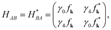
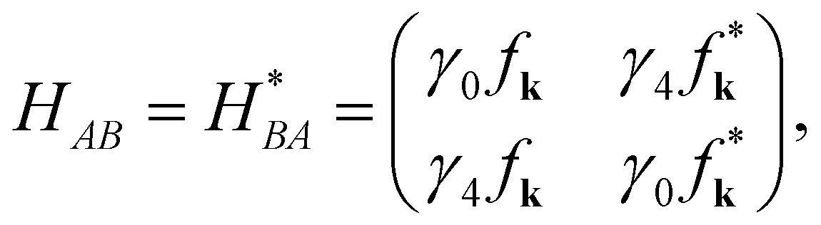
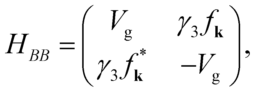
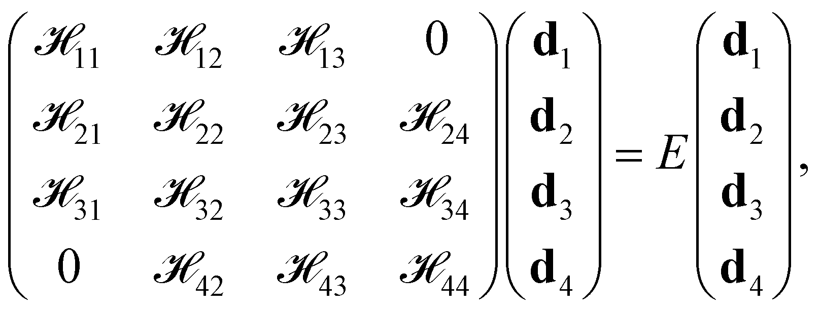
The electronic properties of BBLG subjected to a perpendicular electric field are studied within the tight-binding method framework. The Hamiltonian equation of BBLG is HΦ = EΦ, where the Bloch function is Φ = c1|A1〉 + c2|A2〉 + c3|B1〉 + c4|B2〉, which is the linear combination of the periodic wave functions |A1〉, |A2〉, |B1〉, and |B2〉. HΦ = EΦ is then transformed into the matrix equation H |c〉 = E |c〉, here |c〉 = |c1, c2, c3, c4〉T. The representation of the Hamiltonian matrix reads
| |
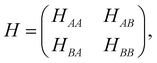 | (1) |
where
H is a 4 × 4 matrix. The elements
HAA,
HAB,
HBA, and
HBB are 2 × 2 matrices. The hopping integrals (
γi) usually used to describe Bernal bilayer graphene are illustrated in the inset of
Fig. 1(a).
γ0 is the intralayer interaction. The hopping integral,
γ1, is the interaction between the dimer sites
A1 and
A2. The trigonal warping integral,
γ3, is the skew interlayer hopping between atoms
B1 and
B2.
γ4 represents
γA1,B2 and
γB2,A1. The matrices
HAA,
HAB and
HBA are further expressed as
| |
 | (2a) |
| |
 | (2b) |
| |
 | (2c) |
where the on-site energy (
Vg) is the electric potential caused by the external perpendicular electric field.

is the structure factor, where
k = (
kx,
ky) is the wavevector and
bl represents the nearest neighbor on the same graphene plane. The three neighboring atoms are located at

,
b2 = (0,
b) and

, and thus

.
To find the analytical energy dispersions of the 4 × 4 matrix above, we now construct the symmetrized basis functions (|ψ1〉, |ψ2〉, |ψ3〉, |ψ4〉)T, which are linear combinations of the periodic wave functions |A1〉, |A2〉, |B1〉, and |B2〉. The symmetrized basis functions are
| |
 | (3) |
where the coefficients
s±1 and
s±2 are the components of the eigenvector of the matrix
HAA (
eqn (2a)). The eigen-equation of
HAA is
| |
 | (4) |
where the eigenenergy is

. The related eigen-vectors (
s±1,
s±2)
T are
| |
 | (5) |
Similarly, the eigenenergy related to
HBB is

.
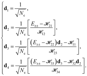
The Bloch function, spanned by the new basis functions (|ψ1〉, |ψ2〉, |ψ3〉, |ψ4〉)T, is Φ = d1|ψ1〉 + d2|ψ2〉 + d3|ψ3〉 + d4|ψ4〉. According to the symmetrized basis functions |ψi〉, the matrix equation has the form
| |
 | (6) |
where the matrix elements are
![[script letter H]](https://www.rsc.org/images/entities/char_e142.gif) ij
ij = 〈
ψi|
H|
ψj〉.The diagonal matrix elements are
| |
 | (7a) |
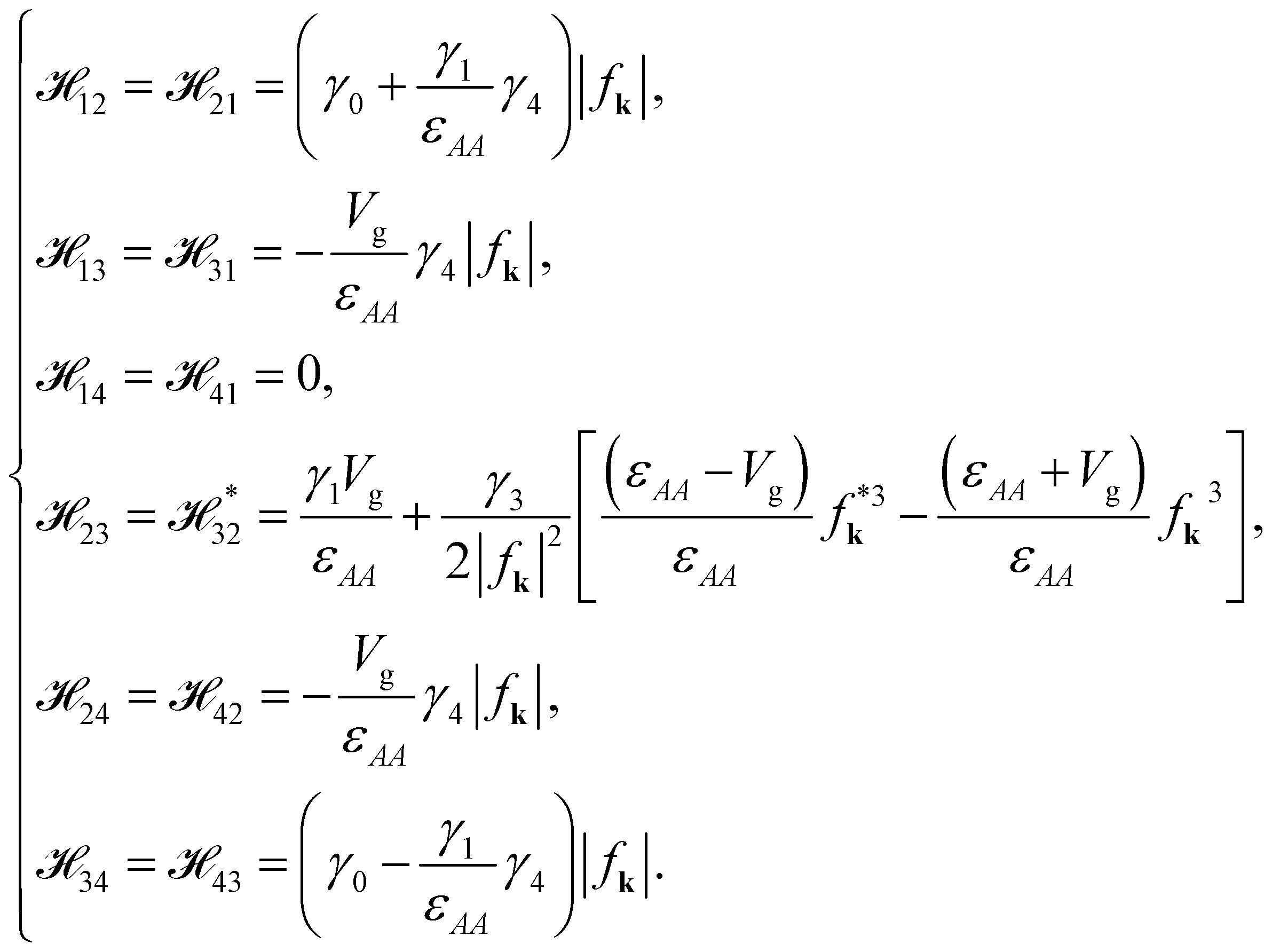
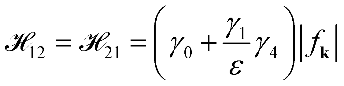
The off-diagonal terms are
| |
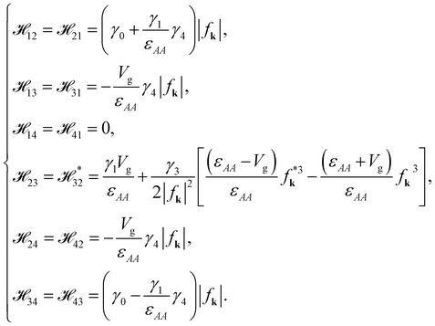 | (7b) |
Notably, in the absence of the gated bias,
Vg = 0,
13,
31,
24 and
42 are all equal to zero.
38 Moreover, a straightforward calculation shows that
222 +
2332 =
εBB2 =
Vg2 +
γ32|
f|
2 because the sub-matrix
is the transformation of
HBB.
2.1 In the limit of γ4 = 0
The exclusion of electron–hole asymmetry, γ4 = 0, allows us to obtain a simple and exact analytical solution to the energy spectrum. The interactions 13, 31, 24 and 42 in Hred are all equal to zero as γ4 = 0. The reduced Hamiltonian matrix (Hred) is a band-storage matrix and is expressed as follows:| |
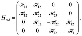 | (8) |
where 12 = 34 = γ0|f(k)|. The analytical energy dispersions, associated with Hred, read| |
 | (9) |
where
where 222 + 2332 = γ32|f|2 + Vg2 is used.  and the angle ϕ is
  . There are four branches of energy bands, which are in the sequence E(k)++ > E(k)+− > E(k)−− > E(k)−+. The former tow, E(k)++ and E(k)+−, are the energy dispersions associated with the conduction bands. The latter two, E(k)−− and E(k)−+ are the energy spectra related to the valence bands.
At the point K, ![[scr B, script letter B]](https://www.rsc.org/images/entities/char_e13f.gif) = γ12/2 + Vg2 and
= γ12/2 + Vg2 and ![[capital script C]](https://www.rsc.org/images/entities/char_e522.gif) = Vg2(γ12 + Vg2). The state energies are exactly E(K) = ±Vg and
= Vg2(γ12 + Vg2). The state energies are exactly E(K) = ±Vg and  . Around the point K and in the absence of the electric field, ≫ and ≈ (γ02|fk|2 − γ1γ3|fk|)2. The two branches of the low energy dispersions of BBLG are
  . They are the eigenenergies of the effective Hamiltonian matrix
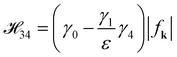
2.2 The effect of γ4 on the energy dispersions
A plainly analytical energy dispersion of the Hamiltonian matrix (eqn (6)), involving all hopping integrals, is in fact inaccessible. The energy dispersions are generally obtained by the numerical diagonalization method. To obtain a simply analytical solution to the energy spectrum, we treat γ4 as a perturbation and neglect the matrix elements 13, 31, 24 and 42 because they make nonsignificant contributions to the energy spectrum. 13, 31, 24 and 42 are right dependent on the magnitude of the gated voltage (Vg) and interlayer interaction (γ4). The magnitude of γ4 is smaller than that of γ0 and γ3, so that 13, 31, 24 and 42 are negligible. γ4 affects the matrix elements 12 and 34 in such a manner as  and
and  . The Hamiltonian equation with the band-storage Hamiltonian matrix is expressed as follows:
| |
 | (10) |
The eigenenergies, determined by the criterion Det|| = 0, are the roots of the secular equation E4 − BE2 − B′E + C = 0, where B = 112 + 222 + 2332 + 122 + 342, B′ = (11 + 22)(122 − 342), and C = 122342 − 1122(122 + 342) + 112(222 + 2332). The analytical form of the eigenenergies looks so complicated and tedious just because the coefficient B′ ≠ 0. To acquire the simple analytical result, we further approximate B′ ≈ 0 because 12 ≈ 34. As a result, the eigenenergies, ε(k), are| |
 | (11) |
To check out the accuracy of the afore-presented model, we first calculate energy dispersions ε(k)±± at Vg = 0 in the high symmetry line K–Γ–M–K, shown by the dashed red curves in Fig. 1(a). There are four energy subbands ε(k)±±. For comparison, energy dispersions, E±±, obtained through the numerical diagonalization of the Hamiltonian matrix (eqn (1)), are also drawn by the black curves in Fig. 1(a). The tight binding parameters (γis) used to calculate the energy bands are: γ0 = −3.12 eV, γ1 = 0.38 eV, γ3 = 0.280 eV, and γ4 = 0.12 eV.39 Obviously, the red curves are not identical to those in black in the higher energy region ε > 3.0 eV. The higher the energy (ε) is, the more discrepancy there is between the two curves. Plus, the energy spectrum ε in the presence of the gated voltage Vg = 200 meV are presented in Fig. 1(b). The applied gated voltage does not significantly affect the profile of energy bands in the high symmetry line K–Γ–M–K. The disagreement between the red and black curves reveals that the derived analytical formula can not exactly describe the energy spectra in the energy region E(eV) > 3.0 eV. Energy dispersions around the point K at different Vgs are shown in Fig. 2 for comparison. The calculation result illustrates that the presented analytical model can not replicate the exact energy dispersions around the point K. Notably, in the absence of the gate voltage, the presented analytical model ε±± can not reproduce the analytical formula of BBLG at Vg = 0.38
 |
| | Fig. 2 The dashed curves are the low energy spectra at different Vgs acquired by eqn (11). For comparison, the energy spectra by numerical diagonalization are drawn in the black curves. | |
We here modify and improve the aforementioned analytical model to approach the exact energy dispersions at any Vg. In the absence of the gated voltage Vg = 0, the matrix elements 23 and 32 in eqn (10) play a minor role and can then be neglected.38 E++ and E−− (E+− and E−+) belong to the symmetrical states (the anti-symmetrical states). E++ and E−− depend only upon 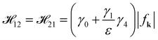 while E+− and E−+ depend on
  .38 We thus replace both 34 and 43 with 12 and 21 in eqn (10) during the calculation of E++ and E−− at any Vg. Then, we obtain the energy dispersions
| |
 | (12a) |
| |
 | (12b) |
where
=
122 + (
112 +
222 +
2332)/2 and
=
124 − 2
1221122 +
112(
222 +
2332). The other two energy bands
E+− and
E−+ are acquired by utilizing
to calculate
′ =
342 + (
112 +
222 +
2332)/2 and
′ =
344 − 2
3421122 +
11(
222 +
2332).
E+− and
E−+ are, respectively, expressed as
| |
 | (12c) |
| |
 | (12d) |
The analytical formulae (eqn (12a–d)) are now employed to calculate the energy dispersions of gated BBLG. We first present the analytical energy dispersions E(k)±± at Vg = 0 in Fig. 3(a). E(k)±± in the high-symmetry line K–Γ–M–K are drawn in red to be distinguished from those obtained through the numerical diagonalization of the Hamiltonian matrix in black. The red curves are exactly identical to the black ones except for the conduction bands in the high-symmetry line KM, where 3.0 eV < E < 3.5 eV (Fig. 3(b)). The energy spectrum in the presence of the gated voltage Vg = 200 meV is also exhibited in Fig. 3(c). The identity between the red and black curves reveals that the derived analytical formula can well describe the energy spectrum of the gated BBLG, except for the conduction bands in the energy region 2.6 eV < E < 3.4 eV (Fig. 3(d)). The results of the calculation show that the analytical model is able to provide us with the exact energy dispersions of the gated BBLG as E < 2.6 eV or E > 3.5 eV. The analytical energy dispersions and conjugated eigenstates are useful for exploring the electronic properties, such as energy dispersions, density of states (DOS), and absorption spectra.
 |
| | Fig. 3 (a) The energy dispersions at Vg = 0 illustrated in the red dashed curves are obtained from the exact analytical model. The black curves are the energy spectra from numerical diagonalization. (b) The conduction bands around the point M. (c) The same plot as in (a) but for Vg = 200 meV. (d) The conduction bands around the point M. | |
3 Discussion: electronic properties
The characteristics of the low energy spectrum are explored. BBLG owns two pairs of parabolic conduction and valence bands, as shown in Fig. 4 in the dashed and solid curves, which are obtained, respectively, by the analytical formulae and the numerical diagonalization method. The dashed curves are in good agreement with the solid curves. With the comparison shown above, the exact solution to the low energy spectrum of BBLG emerges through our analytical model. While the high energy bands arouse some focus of our discussion, we are more interested in the lowest-energy electronic properties. At Vg = 0, E(k)+− and E(k)−+, the first pair located near the chemical potential μ = 0, exhibit a tiny overlap. E(k)+− and E(k)−− are asymmetrical about μ = 0, i.e., electron–hole asymmetry, which is caused by the interlayer interaction γ4. The minimum of E(k)+− and the maximum of E(k)−+ are located at almost the same wavevector (∼the K point). E(k)+− and E(k)−− along the high symmetry lines Γ–K and M–K are strongly anisotropic, which originates in the vanishing of 23 and 32 in eqn (12a–d) along the line Γ–K.
 |
| | Fig. 4 The dashed and solid curves are energy dispersions obtained from the exact analytical formulae and numerical diagonalization. For comparison, the exact energy dispersions are illustrated by the colored curves. | |
The gated voltage (Vg) has a great influence on the low energy spectrum. First, the low energy subbands are significantly modified by Vg and change from monotonically parabolic dispersions into oscillating ones, referred to as a Mexican hat. Then, the asymmetry between the conduction E(k)+− and the valence E(k)−+ bands along the Γ–K direction about the chemical potential is also enhanced. In addition to the K point, two extra band-edge states emerge in all directions. There exists a band-edge state with the minimum (maximum) energy along the Γ–K direction. The energy difference between the lowest band-edge state of E+−(k) and the highest one of E−−(k) decides the band gap, Eg. The locations of the band-edge state are determined by  and
and  . By taking the main interactions, γ0 and γ1, into consideration, E+− (E−−) has a minimum (maximum) at
where the Fermi velocity (
v) is
ħv = 3
bγ0/2. Therefore, the energy gap is
The size of the band gap,
Eg =
E−+ (
kc) −
E−− (
kv), at first grows rapidly but then gradually declines with the increase in
Vg. Another band-edge state along the
KM direction belongs to the saddle point. Such states are the critical points in the energy-wavevector space and thus have a high DOS.
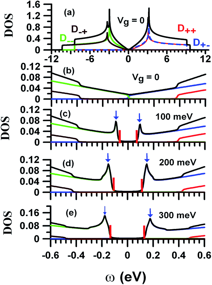
The DOS is useful for understanding the essential physical properties of BBLG. DOS is defined as
| |
 | (13a) |
| |
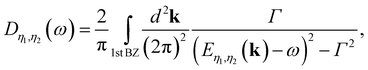 | (13b) |
where
η1,
η2 = ±, ± represents the subband index. The broadening energy width (
Γ) is set as 3.0 meV. The full density of state,
D(
ω), is the summation of
Dη1,η2(
ω), resulting from each subband,
Eη1,η2. The
D(
ω) and
Dη1,η2(
ω) of BBLG at
Vg = 0 are illustrated in
Fig. 5(a). The DOS exhibits logarithmic peaks, originating in the saddle point
M around
ω = ±3 eV, which directly reflects the main features of the energy dispersions. The detailed structure of the DOS at low energy is presented in
Fig. 5(b).
D+−(
ω) (
D−+(
ω)) makes contributions to
D(
ω) as 0 <
ω <
γ1 (−
γ1 <
ω < 0). BBLG at
Vg = 0 is a semi-metal due to the non-vanished DOS at
ω = 0. The gated voltage (
Vg) can open a band gap and induce two van Hove singularities in the energy region −
γ1 <
ω <
γ1, as shown in
Fig. 5(c–e), where the band gap is labeled by vertical red bars and van Hove singularities are indicated by the blue arrows. One can modulate the band gap in BBLG using an external electric field. The increase in
Vg not only enlarges the size of the band gap, but also enhances the height of van Hove singularities. The predicted size of the band gap and locations of van Hove singularities can be verified by experimental measurements.
 |
| | Fig. 5 (a) DOS Dη1η2, associated with each subband Eη1η2, of BBLG at Vg = 0. (b)-(e) are the low-energy DOS at Vg = 0, 100, 200, and 300 meV. The vertical red bars indicate the energy band gap. The blue arrows label the van Hove singularities in the DOS. | |
4 Absorption spectra
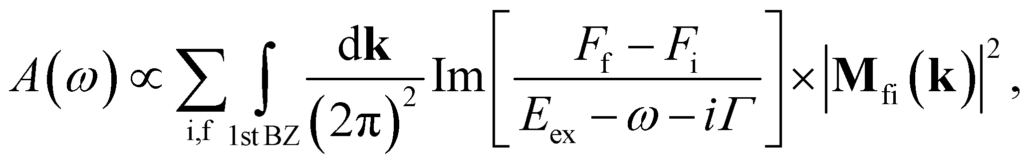
Utilizing the analytical model, we revisit the low-energy absorption spectra of gated BBLG, which has been studied through numerical methods.40–42 The absorption function of bilayer graphene at zero temperature (T = 0) is given by38| |
 | (14) |
where Γ is the broadening parameter owing to various nonradiative processes, f (i) denotes the final (initial) state and Ff (Fi) is the Fermi-Dirac distribution function. Eex = Ef(k) − Ei(k) is the excitation energy.  , the dipole matrix element, is the velocity operator between the initial and final wave functions Φi(k) and Φf(k). The absorption spectrum Ax(ω) originates in electronic transitions that correspond to excitations from the occupied valence bands to the unoccupied conduction bands, excited by the electromagnetic field. In this work, the direction of the electromagnetic field is assumed to be parallel to the x-axis. Within the gradient approximation,43,44 the dipole matrix element
  , where
  is derived from the gradient of the Hamiltonian operator,
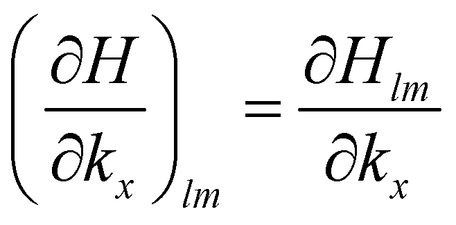
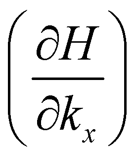
  . Because of the zero momentum of photons, the optical selection rule is Δk = 0. The optical transition channels are determined by the thermal factor FF − Fi and the dipole matrix element.
The dipole matrix element, by inserting the tight-binding wave functions Φ = c1|A1〉 + c2|A2〉 + c3|B1〉 + c4|B2〉, is expressed as
| |
 | (15a) |
where

and
Hlm is the element of the Hamiltonian matrix (
eqn (1)). After the action of the rotation operator (
eqn (3)), the dipole matrix element is then changed into
| |
 | (15b) |
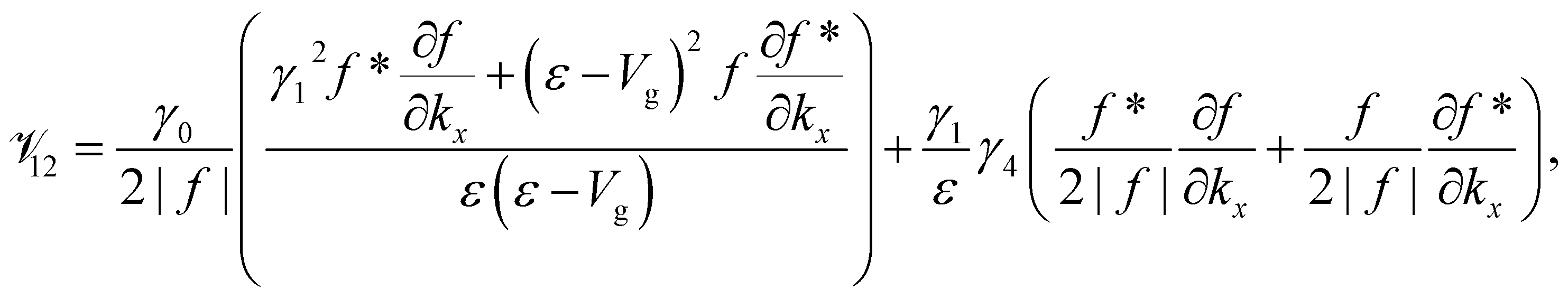
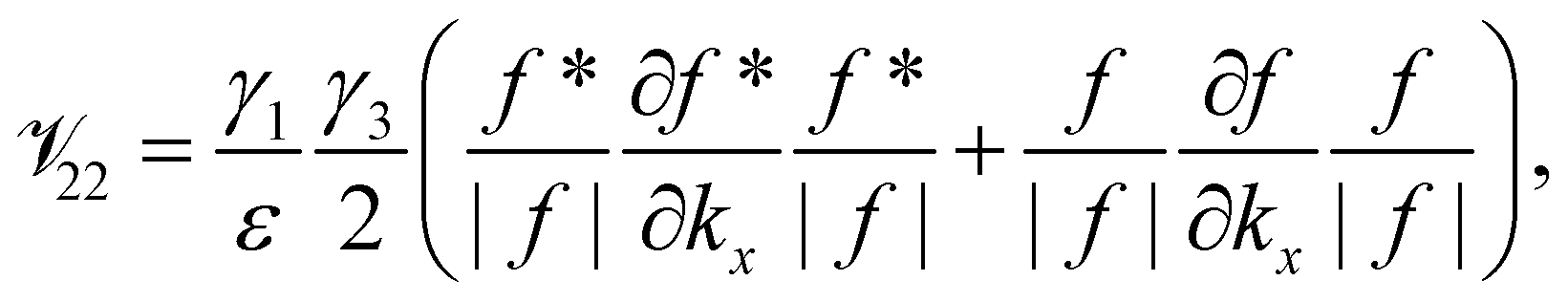
where the analytical form of the matrix element
![[scr V, script letter V]](https://www.rsc.org/images/entities/char_e149.gif) lm
lm is given explicitly in the Appendix. |
di,f1,
di,f2,
di,f3,
di,f4〉 are the initial (final) eigenstates associated with the Bloch function,
eqn (6). The eigenstate corresponding to each energy dispersion (
E±±) can be exactly specified as
| |
 | (16) |
The analytical expression for the dipole matrix element can be used to efficiently evaluate the magnitude of
Mfi and the optical absorption spectra
A(
ω).
Mfi depends on energy spectrum, velocity operator, and eigenstates.
The square of the absolute value of dipole matrix element |Mfi(k)|2 in the high-symmetry line Γ–K–M for the transition E−− → E+− at different Vgs is drawn in Fig. 6, where the solid (dashed) curves are calculated with the energy spectrum and the eigenstates are obtained through the numerical method (analytical model). The dashed curves are exactly in agreement with the solid ones along the high-symmetry line ΓK, while they exhibit some discrepancy around the point M. In the absence of the gated voltage (Vg = 0), |Mfi(k)|2 exhibits a highly anisotropic characteristic with a maximal value around the point M in the high-symmetry line Γ–K–M. |Mfi| is equal to zero in the line Γ–K, along which the structure factor f(k) is a real number and the matrix elements 23 and 32 in eqn (6) are equal to zero. The 4 × 4 Hamiltonian matrix is decomposed into two 2 × 2 blocks. The eigen-vector corresponding to the final (initial) state is |df〉 = |d1, d2, 0, 0〉 (|di〉 = |0, 0, d3, d4〉). The six matrix elements 13, 23, 24, 31, 32, and 42 are all equal to zero as Im[f(k)] = 0 and Vg = 0. The straightforward calculation exhibits that the magnitude of the dipole matrix element vanishes, i.e., |Mfi| = 0.
 |
| | Fig. 6 (a)-(d) The solid curves are the square of the absolute values of the optical matrix |Mfi|, obtained by the numerical diagonalization method. The same plots obtained using analytical formulae are given in the dashed curves. | |
In the presence of the gated voltage, |Mfi|2 shows different aspects, as illustrated in Fig. 6(b–d). Vg alters the Hamiltonian matrix elements, energy spectrum and eigenstates |di〉 and |df〉. Moreover, the Vg-dependent lms are also modified by the gated voltage. As a result, at Vg = 100 meV, |Mfi|2 (blue solid curve in Fig. 6(b)) around the point M exhibits a different aspect and magnitude. The maximum is located in the vicinity of the point M. The increase in Vg does not alter the profile of |Mfi|2 around the point M. Most importantly, the application of Vg enhances |Mfi|2 in the high-symmetry line KΓ. Vg introduces the non-zero matrix elements 23 and 32 in eqn (6), which mixes the symmetrical and anti-symmetrical wave functions, i.e., the alternation of the eigenstates. Moreover, Vg also produces the six matrix elements 13, 23, 24, 31,32, and 42, being unequal to zero. As a result, Vg intensifies |Mfi|2 in the symmetry line KΓ. Such a characteristic strongly modifies the low energy absorption spectra in the presence of Vg.
The low-energy absorption spectra A(ω) of AB BLG reflect the characteristics of the energy dispersions. There are six possible interband excitations resulting from four branches of energy dispersion. The optical excitation from the subband E−+ to E−− and transition between E+− and E++ are forbidden by the thermal factor Ff − Fi. Four allowed excitations, A1(ω), A2(ω), A3(ω) and A4(ω), are shown by the vertical lines in the inset on the left panel of Fig. 7(a). A1(ω) stems from the transition between the highest valence subband (E−−) and the top conduction subband (E++), and A2(ω) originates in the excitation E−+ → E+−. Moreover, the transition from the subband E−− to E+− generates the spectra A3(ω) and the excitation between the subbands E−+ and E++ leads to A4(ω). A1(ω) [A2(ω)] shows a discontinuous structure at ω ≈ 380 meV, as illustrated in Fig. 7(a). Such an optical gap originates in the interband transition between the E−− and E++ subbands [E−+ and E−+ subbands]. A4(ω), resulting from the transition from the E−+ to E++ subband, exhibits an absorption edge at ω ≈ 800 meV. There is no optical gap found in the spectra A3(ω) (red curve) because of the overlap between subbands E−− and E+−. As a result of the superposition of the sub-spectra, the total spectra exhibit two discontinuities at ω ≈ 380 and ω ≈ 800 meV, and no optical gap is found in A(ω).
 |
| | Fig. 7 (a) A1(ω), A2(ω), A3(ω), and A4(ω), the sub-optical spectra, are shown by the blue, green, red and brown curves. Four allowed optical transitions are indicated by the vertical lines in the inset in the left panel. (b) The low-energy absorption spectra (Ai(ω)) at Vg = 0, 100, 200, and 300 meV are drawn in red, green, brown and blue. (c) The low energy absorption spectra with different tight-binding parameters. | |
The application of Vg has a great effect on the low-energy absorption spectra A3(ω), as depicted in Fig. 7(b). Vg not only opens a band gap, but also gives rise to a sharp peak in A3(ω). In the presence of Vg, the steep rise of the spectra, due to the transition between the band-edge states of E−− and that of the E+− subband in the ΓK direction, can be used to determine the size of the energy gap, Eg. The energy gaps are equal to ω = 0.17, 0.25, and 0.28 eV at Vg = 100, 200, and 300 meV. The first absorption peak is a compound one, consisting of a shoulder on the low energy side and a main peak. The former (shoulders) result from the transition between the E−+ and E+− subbands, denoted by the vertical red arrow in Fig. 4. The excitation indicated by the vertical blue arrow in Fig. 4 brings about the main peak. At Vg = 100, 200, and 300 meV, the main peaks are located at ω = 0.18, 0.30, and 0.35 eV. The main peak is in the logarithmic form, stemming from the saddle point in energy dispersions in the high-symmetry line MK. The frequency of the main peak depends on the magnitude of Vg. These peaks make a blue-shift with the increase in Vg. The height of the first peak also enhances with the increase in Vg because the DOS around the band-edge state of E−+ (E+−) and |Mfi|2 in the high-symmetry line ΓK are enhanced by Vg, as shown in Fig. 5 and 6.
How the tight-binding parameters (γis) influence the low energy absorption spectra (A(ω)) is deliberated. The dashed brown curve in Fig. 7(c) represents A(ω) at Vg = 200 meV, through the analytical model, including all the tight-binding parameters, γ0, γ1, γ3, and γ4. The close of the interlayer interaction γ4 has no effect on A(ω), as shown by the cyan curve in Fig. 7(c). According to eqn (7b), the magnitude of  gradually declines with an increase in Vg. As a result, the absorption spectra at Vg = 200 meV are not affected by the interlayer interaction γ4. A(ω), illustrated by the red curve, exhibits a larger band gap (Eg = 270 meV) and a sharp peak located at ω = Eg as the main intralayer interaction (γ0) and interlayer interaction (γ1) are taken into consideration. Moreover, A(ω) presents a simple feature and weaker intensity of absorption relative to those in the brown curve. The chief cause is that the close of the interlayer interaction γ3 not only changes the energy dispersions and wave functions, but also turns off some optical transition channels.
A comparison of the study results with those obtained through ab initio calculations is made. The analytical formulae can exactly describe four energy dispersions and generate the energy bands with “Mexican hat” structures. Our research demonstrates that the gated voltage, Vg, alters the subband spacing, changes the energy band gap, produces the oscillating bands, and induces more band-edge states. The aforementioned electronic properties, e.g., band feature, tunable band gap, and electric-field-modified oscillating bands, are also produced through the ab initio calculations.41 That is, the electronic properties derived from the analytical model are in qualitative agreement with those given by the ab initio calculations. To be more specific, we quantitatively compared the sizes of the gated tunable band gaps acquired by the two methods. The calculated tunable band gaps, shown in Fig. 8 in the cross symbols, are taken from the ab initio calculations.45 The band gap first increases monotonically as the strength of the electric field increases. Then, the energy gaps saturate to a value Eg ≈ 270 meV when the field strength |F| is greater than 0.2 V Å−1. We now evaluate Eg by employing the analytical model for γ3 = γ4 = 0 (black curve) and γ3 ≠ 0 and γ4 ≠ 0 (red curve). The red curve exhibits that Eg first increases sublinearly when the strength of the electric field (|F| = 2Vg/c and c is the layer distance) is less than 0.05 V Å−1. Meanwhile, the energy gaps approach a value of Eg ≈ 300 meV when |F| > 0.2 V Å−1. The behavior of Eg predicted by the analytical method (red curve) is similar to that of the ab initio method. The comparison between the black and red curves illustrates that when the field strength is weaker than 0.05 V Å−1, the tunable band gaps are independent of the hopping integral γ3. After that, the hopping integral γ3 reduces the size of Eg.
 |
| | Fig. 8 The cross symbols are band gaps acquired through the ab initio calculations (data are taken from APL 98, 2011, 263107). Eg is obtained from the analytical model for γ3 = γ4 = 0 (black curve) and γ3 ≠ 0 and γ4 ≠ 0 (red curve). | |
5 Conclusions
We develop a method to access the analytical form of the energy spectrum and eigenstates of gated BBLG within the tight-binding model with all the tight-binding parameters included. The trigonal warping (γ3) and applied gated bias (Vg) destroy the mirror symmetry of BBLG. To deal with the broken symmetry caused by γ3 and Vg, a new set of tight-binding basis functions is constructed through a rotation operator. The renormalized intralayer and interlayer interactions exhibit a gated bias dependence. Most importantly, the Hamiltonian matrix (H) is transformed into a band-storage matrix in the subspace spanned by the new basis functions. The formulae of the energy dispersions and wave functions are then obtained analytically. γ4, the electron–hole asymmetry, is treated as a perturbation and included in the analytical formula. The electronic properties, density of states, optical dipole matrix element and optical absorption spectra are explored by employing this analytical formula. The study shows that Vg can open an optical gap and produce a profound low-energy peak in the absorption spectra. The dipole matrix element (M) and absorption spectra are strongly modified by Vg. Finally, the characteristics of the absorption spectra, e.g., the location and height of the low-energy peak, are significantly presented and explored through the analytical model.
Appendix
The element lm is the operator  sandwiched by the symmetrized basis functions 〈ϕl| and |ϕm〉, i.e.
 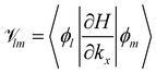 , where H is the Hamiltonian representation (eqn (1)). The analytical form of each lm is listed as follows.
| 11 = 0, |
| 14 = 0, |
| 21 = *12, |
| 31 = *13, |
| 32 = *23, |
| 33 = −22, |
| 42 = *24, |
| 34 = *43, |
| 44 = 0. |
Acknowledgements
The authors gratefully acknowledge the support of the Taiwan National Science Council under the Contract no. NSC 101-2112-M-165-001-MY3.
References
- K. S. Novoselov, A. K. Geim, S. V. Morozov, D. Jiang, Y. Zhang, S. V. Dubonos, I. V. Grigorieva and A. A. Firsov, Science, 2004, 306, 666 CrossRef CAS PubMed.
- Y. B. Zhang, Y. W. Tan, H. L. Stormer and P. Kim, Nature, 2005, 438, 201 CrossRef CAS PubMed.
- V. P. Gusynin and S. G. Sharapov, Phys. Rev. Lett., 2005, 95, 146801 CrossRef CAS.
- A. H. Castro Neto, F. Guinea, N. M. R. Peres, K. S. Novoselov and A. K. Geim, Rev. Mod. Phys., 2009, 81, 109 CrossRef CAS.
- N. M. R. Peres, Rev. Mod. Phys., 2010, 82, 2673 CrossRef CAS.
- M. J. Allen, V. C. Tung and R. B. Kaner, Chem. Rev., 2010, 110, 132 CrossRef CAS PubMed.
- D. S. L. Abergela, V. Apalkovb, J. Berashevicha, K. Zieglerc and T. Chakrabortya, Adv. Phys., 2010, 59, 261 CrossRef.
- K. S. Novoselov, V. I. Fal'ko, L. Colombo, P. R. Gellert, M. G. Schwab and K. Kim, Nature, 2012, 490, 192 CrossRef CAS PubMed.
- N. O. Weiss, H. Zhou, L. Liao, Y. Liu, S. Jiang, Y. Huang and X. Duan, Adv. Mater., 2012, 24, 5782 CrossRef CAS PubMed.
- K. S. Novoselov, E. McCann, S. V. Morozov, V. I. Fal'ko, M. I. Katsnelson, U. Zeitler, D. Jiang, F. Schedin and A. K. Geim, Nat. Phys., 2006, 2, 177 CrossRef.
- F. Guinea, M. I. Katsnelson and A. K. Geim, Nat. Phys., 2010, 6, 30 CrossRef CAS.
- S. Das Sarma, S. Adam, E. H. Hwang and E. Rossi, Rev. Mod. Phys., 2011, 83, 407 CrossRef CAS.
- D. A. Abanin, B. E. Feldman, A. Yacoby and B. I. Halperin, Phys. Rev. B: Condens. Matter Mater. Phys., 2013, 88, 115407 CrossRef.
- M. Kim, N. S. Safron, C. Huang, M. S. Arnold and P. Gopalan, Nano Lett., 2012, 12, 182 CrossRef CAS PubMed.
- B. M. Wong, S. H. Ye and G. O'Bryan, Nanoscale, 2012, 4, 1321 RSC.
- G. Cocco, E. Cadelano and L. Colombo, Phys. Rev. B: Condens. Matter Mater. Phys., 2010, 81, 241412 CrossRef.
- Z. H. Ni, T. Yu, Y. H. Lu, Y. Y. Wang, Y. P. Feng and Z. X. Shen, ACS Nano, 2008, 2, 2301 CrossRef CAS PubMed.
- M. Y. Han, B. Ozyilmaz, Y. Zhang and P. Kim, Phys. Rev. Lett., 2007, 98, 206805 CrossRef.
- Y. Zhang, T. T. Tang, C. Girit, Z. Hao, M. C. Martin, A. Zettl, M. F. Crommie, Y. R. Shen and F. Wang, Nature, 2009, 459, 820 CrossRef CAS PubMed.
- A. B. Kuzmenko, I. Crassee, D. van der Marel, P. Blake and K. S. Novoselov, Phys. Rev. B: Condens. Matter Mater. Phys., 2009, 80, 165406 CrossRef.
- T. Thiti and J. H. Pablo, Phys. Rev. Lett., 2010, 105, 166601 CrossRef.
- M. T. Allen, J. Martin and A. Yacoby, Nat. Commun., 2012, 3, 934 CrossRef CAS PubMed.
- C. L. Lu, C. P. Chang, Y. C. Huang, R. B. Chen and M. L. Lin, Phys. Rev. B: Condens. Matter Mater. Phys., 2006, 73, 144427 CrossRef.
- M. Orlita, C. Faugeras, J. M. Schneider, G. Martinez, D. K. Maude and M. Potemski, Phys. Rev. Lett., 2009, 102, 166401 CrossRef CAS.
- E. V. Castro, K. S. Novoselov, S. V. Morozov, N. M. R. Peres, J. M. B. Lopes dos Santos, J. Nilsson, F. Guinea, A. K. Geim and A. H. Castro Neto, Phys. Rev. Lett., 2007, 99, 216802 CrossRef.
- E. V. Castro, K. S. Novoselov, S. V. Morozov, N. M. R. Peres, J. M. B. Lopes dos Santos, J. Nilsson, F. Guinea, A. K. Geim and A. H. Castro Neto, J. Phys.: Condens. Matter, 2010, 22, 175503 CrossRef PubMed.
- Y. H. Ho, Y. H. Chiu, D. H. Lin, C. P. Chang and M. F. Lin, ACS Nano, 2010, 4, 1465 Search PubMed.
- E. McCann and M. Koshino, Rep. Prog. Phys., 2013, 76, 056503 CrossRef PubMed.
- R. Côte and M. Barrette, Phys. Rev. B: Condens. Matter Mater. Phys., 2013, 88, 245445 CrossRef.
- H. Cheraghchi and F. Adinehvand, J. Phys.: Condens. Matter, 2014, 26, 015302 CrossRef PubMed.
- F. Kadi and E. Malic, Phys. Rev. B: Condens. Matter Mater. Phys., 2014, 89, 045419 CrossRef.
- J. Cserti, A. Csordas and G. David, Phys. Rev. Lett., 2007, 99, 066802 CrossRef.
- M. Koshino, New J. Phys., 2009, 11, 095010 CrossRef.
- L. M. Zhang, M. M. Fogler and D. P. Arovas, Phys. Rev. B: Condens. Matter Mater. Phys., 2011, 84, 075451 CrossRef.
- C. P. Chang, J. Appl. Phys., 2011, 110, 013725 CrossRef PubMed.
- C. P. Chang, Carbon, 2013, 61, 209 CrossRef CAS PubMed.
- J. C. Charlier, J. P. Michenaud and X. Gonze, Phys. Rev. B: Condens. Matter Mater. Phys., 1992, 46, 4531 CrossRef CAS.
- C. P. Chang, J. Appl. Phys., 2012, 111, 103711 CrossRef PubMed.
- K. Nakao, J. Physiol. Soc. Jpn., 1976, 40, 761 CAS.
- C. L. Lu, C. P. Chang, Y. C. Huang, R. B. Chen and M. L. Lin, Phys. Rev. B: Condens. Matter Mater. Phys., 2006, 73, 144427 CrossRef.
- H. Min, B. Sahu, S. K. Banerjee and A. H. MacDonald, Phys. Rev. B: Condens. Matter Mater. Phys., 2007, 75, 155115 CrossRef.
- L. Yang, Phys. Rev. B: Condens. Matter Mater. Phys., 2010, 81, 155445 CrossRef.
- J. G. Johnson and G. Dresselhaus, Phys. Rev. B: Solid State, 1973, 7, 2275 CrossRef.
- F. L. Shyu, C. P. Chang, R. B. Chen, C. W. Chiu and M. F. Lin, Phys. Rev. B: Condens. Matter Mater. Phys., 2003, 67, 045405 CrossRef.
- B. R. Wu, Appl. Phys. Lett., 2011, 98, 263107 CrossRef PubMed.
|
| This journal is © The Royal Society of Chemistry 2014 |
Click here to see how this site uses Cookies. View our privacy policy here. 
 , and M at
 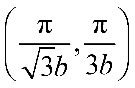 .
.


 is the structure factor, where k = (kx, ky) is the wavevector and bl represents the nearest neighbor on the same graphene plane. The three neighboring atoms are located at
  , b2 = (0, b) and
  , and thus
 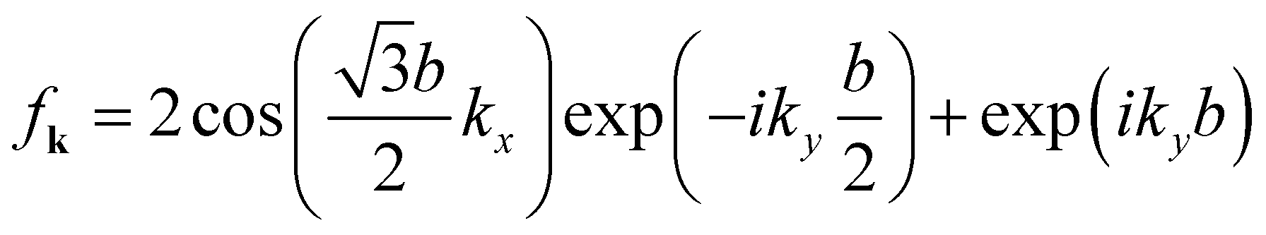 .
.


 . The related eigen-vectors (s±1, s±2)T are
 .
.


 and the angle ϕ is
 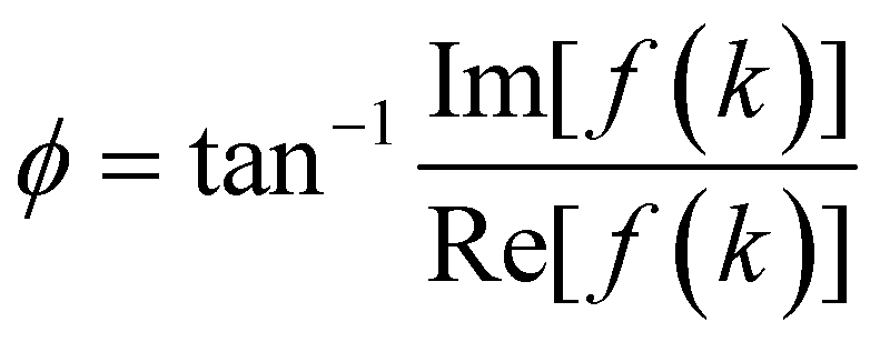 . There are four branches of energy bands, which are in the sequence E(k)++ > E(k)+− > E(k)−− > E(k)−+. The former tow, E(k)++ and E(k)+−, are the energy dispersions associated with the conduction bands. The latter two, E(k)−− and E(k)−+ are the energy spectra related to the valence bands.
 . Around the point K and in the absence of the electric field,
  . They are the eigenenergies of the effective Hamiltonian matrix
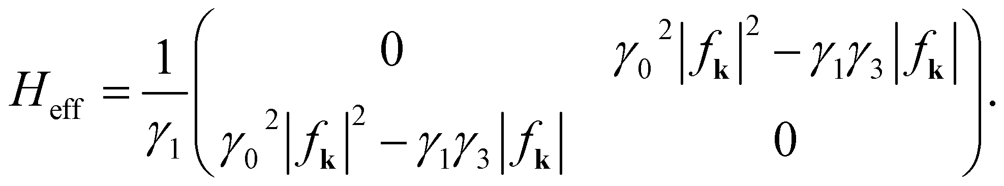
 and
and 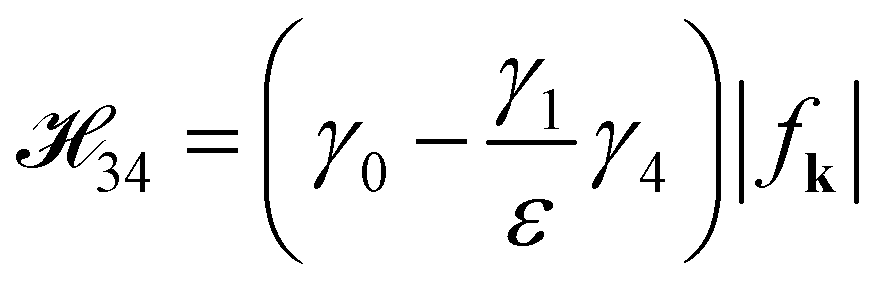 . The Hamiltonian equation with the band-storage Hamiltonian matrix is expressed as follows:
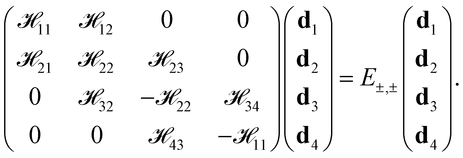


 while E+− and E−+ depend on
  .38 We thus replace both

 to calculate
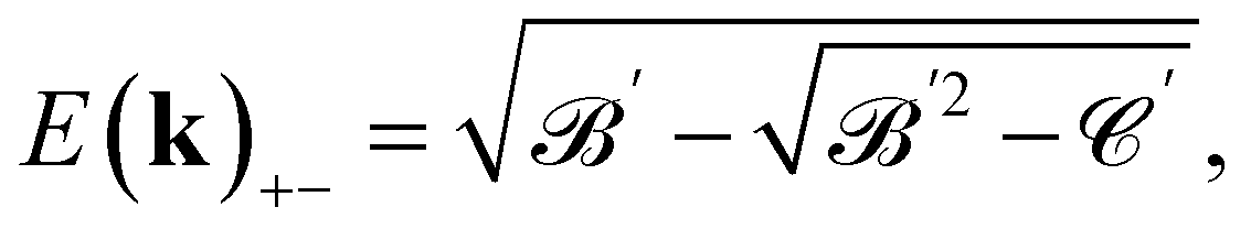


 and
and  . By taking the main interactions, γ0 and γ1, into consideration, E+− (E−−) has a minimum (maximum) at
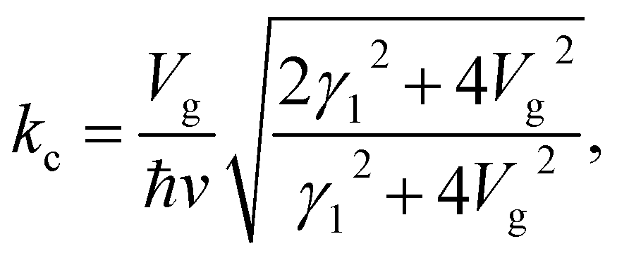


 , the dipole matrix element, is the velocity operator between the initial and final wave functions Φi(k) and Φf(k). The absorption spectrum Ax(ω) originates in electronic transitions that correspond to excitations from the occupied valence bands to the unoccupied conduction bands, excited by the electromagnetic field. In this work, the direction of the electromagnetic field is assumed to be parallel to the x-axis. Within the gradient approximation,43,44 the dipole matrix element
  , where
  is derived from the gradient of the Hamiltonian operator,
  . Because of the zero momentum of photons, the optical selection rule is Δk = 0. The optical transition channels are determined by the thermal factor FF − Fi and the dipole matrix element.

 and Hlm is the element of the Hamiltonian matrix (eqn (1)). After the action of the rotation operator (eqn (3)), the dipole matrix element is then changed into
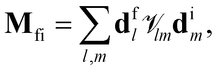


 gradually declines with an increase in Vg. As a result, the absorption spectra at Vg = 200 meV are not affected by the interlayer interaction γ4. A(ω), illustrated by the red curve, exhibits a larger band gap (Eg = 270 meV) and a sharp peak located at ω = Eg as the main intralayer interaction (γ0) and interlayer interaction (γ1) are taken into consideration. Moreover, A(ω) presents a simple feature and weaker intensity of absorption relative to those in the brown curve. The chief cause is that the close of the interlayer interaction γ3 not only changes the energy dispersions and wave functions, but also turns off some optical transition channels.
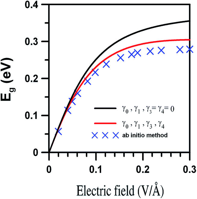
 sandwiched by the symmetrized basis functions 〈ϕl| and |ϕm〉, i.e.
  , where H is the Hamiltonian representation (eqn (1)). The analytical form of each