Ternary alloy nanocrystals of tin and germanium chalcogenides†
Hyung Soon Im,
Yoon Myung,
Kidong Park,
Chan Su Jung,
Young Rok Lim,
Dong Myung Jang and
Jeunghee Park*
Department of Chemistry, Korea University, Jochiwon 339-700, Korea. E-mail: parkjh@korea.ac.kr
First published on 21st March 2014
Abstract
Tin (Sn) and germanium (Ge) chalcogenides have recently gained popularity as potential alternatives to the toxic lead chalcogenides, due in part to their relatively higher chemical and environmental stability, for use in photovoltaic devices. Herein, we report the synthesis of ternary composition chalcogenide, i.e., SnxGe1−xS, SnxGe1−xSe, GeSxSe1−x, and SnSxSe1−x, nanocrystals (NCs) by novel gas-phase laser photolysis. A full series of completely miscible alloy nanocrystals, the band gaps of which could be tuned to cover a wide range (0.9–1.6 eV), were obtained by facile composition tuning through adept control of the relative pressure of the precursors. Two cation alloy (SnxGe1−xS and SnxGe1−xSe) NCs exhibited unique anisotropic bowing phenomena of the orthorhombic phase lattice constants, but the anion alloy (GeSxSe1−x and SnSxSe1−x) NCs did not. The cation alloy NCs showed optical bowing, which is well correlated with the bowing of the lattice parameters. The SnxGe1−xS and SnSxSe1−x NCs showed remarkably higher photoconversion efficiency in photovoltaic and photodetector devices when compared with that of end members.
Introduction
IV–VI chalcogenide semiconductor nanocrystals (NCs) have attracted considerable attention in photovoltaic applications owing to their unique size-dependent optical and electrical properties.1–4 Recently, there has been increased interest in the ternary alloys of IV–VI chalcogenide semiconductors, as they offer the exceptional advantage of modifying the properties of semiconductors for specific applications. In particular, alloying is considered to be an effective strategy in solar energy conversion devices for controlling the conduction band gap offsets and/or localized defect energy levels, which is critical for achieving high photoconversion efficiency. However, it is highly challenging to realize homogeneous alloys because of the inherent differences in precursor reaction kinetics, which require adept control of the reactivity of individual precursors. Thus far, limited success has been reported in the following systems: PbSSe, PbSnTe, PbSnS, PbSTe, PbSeTe, SnSSe, GeSSe, and SnGeSe.5–19Lately, tin and germanium chalcogenides (SnS, SnSe, GeS, and GeSe) have gained popularity as potential alternatives to the conventional lead chalcogenides in part because of their relatively higher chemical and environmental stability as compared to more toxic lead chalcogenides. Typically, tin and germanium chalcogenides possess a thermodynamically preferred orthorhombic crystal structure, described as a highly distorted rock salt structure consisting of strongly bound double layers held by a weaker van der Waals force. They are native p-type semiconductors with high absorption coefficient, and narrow band gap; the band gap of bulk materials being Eg = 1.5–1.6 eV (GeS), 1.1–1.2 eV (GeSe), 1.1 eV (SnS), and 0.9 eV (SnSe).20–25 The band gaps of SnGeS, SnGeSe, SnSe, and GeSSe alloys covered the wide range of 0.9–1.6 eV. Recently, Wei et al. synthesized SnSxSe1−x NCs using a solution reaction of SnO2, S, and Se.16 Brutchey and co-workers reported the synthesis of composition-tuned SnxGe1−xSe NCs in solution phase.18 Nevertheless, development of facile strategies for controlling the composition of both cation and anion alloys is still a critical requirement.
In the present work, we demonstrate the successful synthesis of ternary alloy series; SnxGe1−xS, SnxGe1−xSe, GeSxSe1−x, and SnSxSe1−x NCs, with controlled composition over the whole range of 0 ≤ x ≤ 1. The ligand-free NCs were synthesized by the gas-phase laser photolysis method, wherein the composition of the NCs could be easily tuned by controlling the partial pressure of the reactant mixture. This method has previously been adopted for the synthesis of anion alloy NCs.17,19 Herein, we extend this method to the composition tuning of cation alloys, which has not been attempted yet. Thus far, several researchers have analyzed the optoelectronic properties of GeSe, SnS, and SnSe nanostructures, including nanosheets and nanowires, demonstrating their promising potential in photovoltaic applications.26–39 We report here the enhanced photoconversion efficiency of the alloy NCs in photoelectrochemical (PEC) cells and photodetector devices when compared with that of the binary counterparts. In order to understand such an enhancement effect, we thoroughly examined the dependence of the lattice parameters and optical band gap on the composition. We believe that the results obtained in this study will pave the way for the development of frontier photovoltaic devices.
Experimental section
Laser photolysis of (Ge(CH3)4, TMG), tetramethyl tin (Sn(CH3)4, TMT), hydrogen sulfide (H2S), and dimethyl selenium (Se(CH3)2, DMS) was performed using an Nd:YAG pulsed laser (Coherent) operated at 1064 nm, with a repetition rate of 10 Hz and a pulse width of 10 ns. All the precursors were purchased from Sigma-Aldrich or Alfa Co. The precursors were degassed by several freeze (77 K)–pump–thaw cycles, and used without further purification. In the typical process, the precursor vapors (<300 Torr) were introduced to a Pyrex glass reactor, equipped with a gas valve connected to a standard vacuum line and a quartz optical window. The laser beam was focused into the reactor through the quartz window, by using a lens of focal length 10 cm. The experiment was carried out using the photon energy of 0.1–0.2 J per pulse. After 1 h of laser irradiation, the gas products were vented out. Subsequently, the NCs were collected by dispersing them in ethanol, followed by evaporation and vacuum drying at room temperature. In order to obtain the crystalline phase, the obtained NC powders were thermally annealed in a quartz tube under vacuum at 350–450 °C for 1 h.Graphene oxide (GO) was synthesized from graphite by Hummer's exfoliation method, which was further reduced using H2 gas at 800 °C to obtain reduced GO (RGO). The NC–RGO hybrid nanostructures were subsequently prepared by mixing NCs with RGO in isopropyl alcohol (IPA) under sonication, and then precipitated and dried. The average thickness of the RGO sheets, as determined by using AFM (Park System XE100), was 6 nm.
The samples were characterized by scanning electron microscopy (SEM, Hitachi S-4700), field-emission transmission electron microscopy (TEM, Jeol JEM 2100F and FEI TECNAI G2 200 kV), high-voltage TEM (HVEM, Jeol JEM ARM 1300S, 1.25 MV), and energy-dispersive X-ray spectroscopy (EDX). High-resolution X-ray diffraction (XRD) patterns were obtained using the 9B and 3D beam lines of the Pohang Light Source (PLS) with monochromatic radiation (λ = 1.5474 Å). UV-visible-NIR absorption spectra of the samples were recorded using a spectrometer (Cary 5000, Agilent Tech.). The Raman spectra were measured using the 514.5 nm line of an argon ion laser.
The cyclic voltammetry (CV) curves were recorded on an IVIUM CompactStat electrochemical analyzer using gold (area ca. 0.02 cm2) disks as the working electrode, Pt-wire as auxiliary electrode and Ag/0.01 M AgNO3 as reference electrode (BAS Inc., 0.1 M tetrabutylammonium hexafluorophosphate (TBAPF6)/acetonitrile electrolyte). The NC solution was prepared by dispersing 1 mg of NC in 1 mL of IPA. Approximately a drop of the NC solution was placed on the polished surface of the working electrode, and the solvent was then evaporated to form a film. The electrolytes were thoroughly deoxygenated by bubbling with high-purity Ar gas for 15 min. The valence band (VB) and conduction band (CB) energies, EVB and ECB, respectively, can be calculated from the voltage values corresponding to the onset of oxidation peak (EOx) and reduction (ERed) peak, assuming the energy level of ferrocene/ferrocenium (Fc/Fc+) to be −4.8 eV below the vacuum level. The formal potential of Fc/Fc+ was measured to be 0.085 V against an Ag/Ag+ reference electrode, providing the calibration equations, EVB = −(EOx + 4.715) eV; ECB = −(ERed + 4.715) eV.
Transient photocurrents of the photoelectrochemical (PEC) cells were measured in a three-electrode setup composed of 0.5 M sodium sulfate (Na2SO4) aqueous electrolyte, Pt foil counter electrode, and Ag/AgCl reference electrode (Aldrich, 3 M KCl). In the typical process, 100 mg of the NCs was dissolved in 5 mL of IPA. Typically, about 60 min of ultrasonication was necessary to obtain uniformly dispersed solution. The NC film was fabricated by dropping 100 μL of the NC solution onto an area of 0.25 cm2 in the ITO substrate, followed by drying under ambient conditions. A constant light intensity of 100 mW cm−2 from a 450 W Xe lamp (Oriel) passed through an AM 1.5G filter was used as the light source. The photo-response of the NC films was applied at −0.5 V vs. Ag/AgCl at 10 s on/off chopped illuminations.
The Ti (20 nm)/Au (80 nm) film electrode was deposited onto a Si substrate with a thermally grown SiO2 layer of thickness 1 μm, by sputtering using a patterned mask. The gap between the electrodes was 1.5 μm. The photodetector was then fabricated by using the dielectrophoresis (DEP) technique. We tested the devices on the probe station with parametric test equipment (Agilent E5270A) at room temperature, using 514 nm Ar ion laser (2–20 mW) or light emitting diode (LED) operating at 850 nm (max. 170 mW) as the light source.
Results and discussion
Table S1 (ESI†) summarizes the partial pressure of the precursors for all the NCs (total 56 samples) prepared in the present work. The overall morphology was observed by using TEM (Fig. 1a). The NCs exhibit a size distribution with an average diameter of 10 ± 3 nm. Fig. 1b shows the lattice-resolved and corresponding fast-Fourier transform (FFT) images (zone axis = [110]) of orthorhombic phase Sn0.6Ge0.4S. The d-spacing of the (110) planes is estimated to be 4.0 Å, which is consistent with the value calculated by Vegard's rule using the bulk values dSnS(110) = 4.04 Å and dGeS(110) = 3.97 Å. The EDX line scan profile of Sn (L shell), Ge (L shell), and S (K shell) showed an elemental ratio of 25![[thin space (1/6-em)]](https://www.rsc.org/images/entities/char_2009.gif) :20:55, along the cross section of the NC. Inset corresponds to the scanning TEM (STEM) image of the NCs.
:20:55, along the cross section of the NC. Inset corresponds to the scanning TEM (STEM) image of the NCs.
 | ||
| Fig. 1 (a) HRTEM image revealing the spherical shape of Sn0.6Ge0.4S NCs. The average diameter is 10 nm. (b) Lattice-resolved and FFT images (at the zone axis of [110]) of selected orthorhombic phase NCs shows d110 = 4.0 Å. (c) EDX line-scan profile showing the homogeneous distribution of the elements Sn, Ge, and S along the cross section of NC (whose STEM is shown in the inset) in a ratio of 25:20:55. | ||
Fig. S1 (ESI†) shows the XRD patterns of the NCs. The peaks were assigned to those of orthorhombic phase with a Pnma or Pbnm space group. The composition (x) of alloy NCs was determined using Vegard's law (i.e., d = (1 − x)dGeS + xdSnS) based on the peak position of the end members. For this, approximately 5–8 high-intensity peaks were selected to calculate the composition, and their average value was determined as x. The x value was found to be consistent with the corresponding EDX data shown in the Fig. S2 and S3 (ESI†). The composition of the NCs can be well correlated with the partial pressure of the precursors (ESI,† Fig. S4). We obtained the lattice parameters of the end members (in a notation of Pnma), which is consistent with the reference values; a = 10.47 Å, b = 3.64 Å, c = 4.29 Å for GeS; a = 11.21 Å, b = 3.98 Å, c = 4.29 Å for SnS; a = 10.83 Å, b = 3.84 Å, c = 4.38 Å for GeSe; a = 11.52 Å, b = 4.16 Å, c = 4.42 Å for SnSe.
Fig. 2 shows the lattice constants (a, b, and c) and the unit cell volume plotted as a function of x. In case of cation alloy (SnxGe1−xS and SnxGe1−xSe) NCs, all three lattice constants varies nonlinearly with x. The deviation from a linear fit line (as drawn by a line) is called the “bowing” phenomenon. Analysis of this phenomenon in the present study using high-resolution synchrotron XRD clearly revealed the deviation. All data points an uncertainty of 5–10%. The lattice constants a and b are larger than their linear values in the Sn-rich composition (x > 0.5), which is referred to as “upward bowing”. The magnitude of the deviation is larger for the SnxGe1−xS NCs than for the SnxGe1−xSe NCs. In contrast, the c lattice constant shows a deviation in the opposite direction (referred to as “downward bowing”). It should be noted that the plots of the c lattice constant exaggerate its non-linear change owing to the smaller differences of binary counterparts (GeS–SnS and GeSe–SnSe). For SnxGe1−xS NCs, the maximum deviations from the linear values occurs at x = 0.7 with Δa = 0.08 Å, Δb = 0.04 Å, and Δc = −0.02 Å. The maximum value of deviation in the lattice constants of SnxGe1−xSe NCs is Δa = 0.05 Å, Δb = 0.02 Å, and Δc = −0.03 Å, at x = 0.8. The deviation of the c lattice constant was previously observed for the SnxGe1−xSe NCs and bulk materials.18,40 The positive deviation (sum of Δa and Δb) is constantly larger than the negative deviation (|Δc|) for both NCs. As a result, the SnxGe1−xS NCs exhibit noticeably upward bowing in the unit cell volume, corresponding to the volume expansion. In the case of the SnxGe1−xSe NCs, the unit cell volume is changed almost linearly with x, owing to the less expansion of the a and b lattice constants compared to that of the SnxGe1−xS NCs.
 | ||
| Fig. 2 Dependence of the lattice constants (a, b, and c) and unit cell volume on Sn content (x) in (a) SnxGe1−xS and SnxGe1−xSe NCs, and on S content (x) in (b) GeSxSe1−x and SnSxSe1−x NCs. | ||
Surprisingly, the GeSxSe1−x and SnSxSe1−x NCs showed no bowing in the lattice constants or the unit cell volume. This “no bowing” phenomenon of the SnSxSe1−x NCs is consistent with previous reports.16,41 We concluded that the bowing of the lattice parameters exists in the cation alloy NCs. Both the SnxGe1−xS and SnxGe1−xSe NCs exhibit consistently anisotropic bowing: the upward bowing for the a and b constants and the downward bowing for the c constant in the range of x > 0.5. The dominant expansion of the lattice parameters upon the Sn-rich alloy formation was exclusively observed for these NCs. Furthermore, we used Raman spectroscopy to confirm the homogeneity of alloying (see ESI,† Fig. S5).
As mentioned in the Introduction section, the double layer-type orthorhombic crystal structure can be described as a deformed rock salt structure. The interatomic distance perpendicular to these layers (a-axis) is larger than that along them (b- and c-axis). The deformation from the ideal rock-salt lattice is the greatest for the c-axis.42,43 As a consequence, there exists considerable anisotropy of the physical properties. It was found that the location and nature of the band gap depends on the tightly bound crystallographic b- and c-axes; their indirect band gap is smaller for the c-axis than for the b-axis (i.e., 1.542 versus 1.572 eV for GeS and 1.095 versus 1.142 eV for SnS).20,21 Recent calculations showed a strong anisotropic band offset of SnS–GeS hetero-junctions.44
The anisotropic bowing of the lattice constants is probably a result of the crystallographic anisotropy. The c-axis encloses the non-polar surface unlike the a- and b-axes. The bonding of the Sn–S lattice is more ionic than that of the Ge–S lattice.45 Therefore, the incorporation of Sn into the Ge–S (or GeSe) lattices would be more favorable in polar a- and b-axes, such that the lattice constants a and b become larger than the linear value, whereas the c lattice constant reduces. As the Sn composition increases, the preference of the Sn–S bonds along the a- and b-axes would cause the expansion of the unit cell volume of SnxGe1−xS. For the SnxGe1−xSe, the expansion of the a and b lattice constants occurs by the less magnitude than that of the SnxGe1−xS, probably due to the more covalent character of GeSe–SnSe. No bowing phenomena of the anion alloys can be rationalized by the similar bonding nature of S and Se anions toward the same cations. For the bowing of the lattice constant of cubic phase crystals, Fong et al. suggested a model in which the bond-stretching or -bending force constants of the two constituents are critical to determine the curve shape.46 In order to explain the anisotropic bowing curves of the orthorhombic phase crystals using the force constants, a finer model is probably necessary.
In addition, the optical band gap of all NC samples prepared in this study was estimated by using UV-visible-near IR (NIR) diffuse reflectance spectrum. The composition tuning enables the band gap to show absorption in the NIR region of 800–1400 nm (0.9–1.6 eV). Based on Kubelka–Munk (K–M) transformation, the plot of [F(ν)hν]1/2 and [F(ν)hν]2 (where F(ν) is the diffuse reflectance spectrum) versus photon energy yielded the indirect and direct band gaps, respectively (see the ESI,† Fig. S6 and Table S2).27,38,39,47 The indirect band gap (Eg) is plotted in Fig. 3a. All these have uncertainty of at least 5% that comes from the extrapolation process of the linear region. The Eg value of GeS (1.57 eV), SnS (1.23 eV), GeSe (1.20 eV), and SnSe (0.92 eV), is consistent with the reported value of the NC, respectively, 1.58 eV,27 1.18 eV,32 1.14 eV,27 and 0.9 eV (size = 9 nm).36 It is known that the bulk SnS exhibits a high absorption coefficient and excellent hole mobility with a direct band gap of 1.3 eV.48,49 The plot of [F(ν)hν]2 provides a direct band gap to be 1.25 eV, which is close to the value of the bulk. The steep rise of the absorption onset could be another evidence for the contribution of direct band gap. The small quantum confinement effects are probably due to the diameter being larger than the Bohr radius (e.g., 7 nm for SnS).32
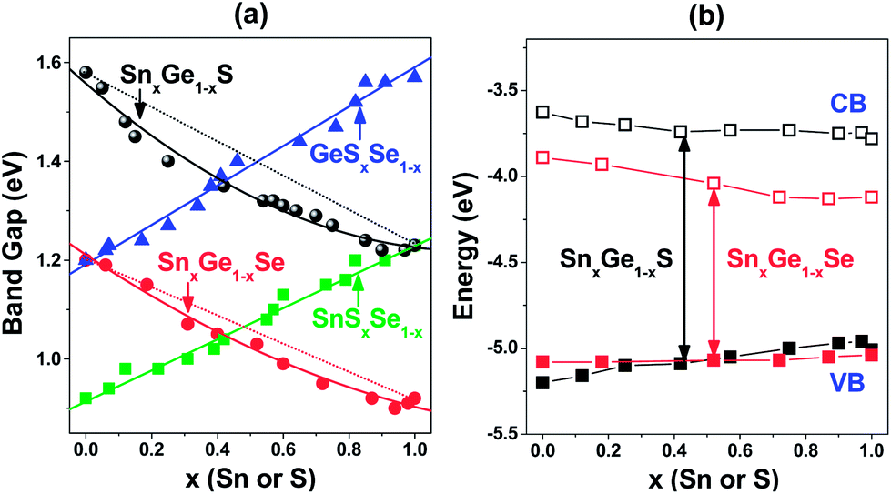 | ||
| Fig. 3 (a) Dependence of the optical band gap on the content (x) of Sn or S, and (b) the band energy (VB and CB) diagram (versus vacuum level) of SnxGe1−xS and SnxGe1−xSe, which was estimated from the oxidation peaks of CV and optical band gap. | ||
The SnxGe1−xS NCs show a non-linear dependence of Eg on the composition, which deviates from the linear value, predicted using Vegard's law. This optical bowing is characterized by a positive bowing constant b (= 0.25 eV), where Eg(x) = (1 − x)Eg(GeS) + xEg(SnS) – bx(1 − x). The SnxGe1−xSe NCs also show the optical bowing with b = 0.14 eV, which is less than that of the SnxGe1−xS NCs. On the other hand, the anion alloys, GeSxSe1−x and SnSxSe1−x, NCs show no optical bowing; Eg changes almost linearly with the composition. Remarkably, the more significant bowing of the band gap appears in the SnxGe1−xS NCs that possess noticeably the expanded unit cell volume, which suggests that the optical bowing could be correlated with the bowing of the lattice parameters.
Zunger and coworkers explained the optical bowing of semiconductor alloys using the structure and electronic factors, which include the volume deformation of the band structure due to different lattice constants of the binary structures.50–53 Recently, Wu et al. reported the calculation on the optical bowing (b > 0) for the Cd1−xZnxS cation alloy that is dominated by volume deformation.54 There is no calculation to support the bowing phenomena of the Ge–Sn chalcogenide series. Thus, we are under theoretical investigation to rationalize the experimental results. Nevertheless, our results prove that the optical bowing of the cation alloy NCs is robustly related to the deformed volume; the expansion of the lattice parameters decreased the band gap, which is consistent with the general trend of II–VI semiconductor alloys.50,51,54
The cyclic voltammetric (CV) results were used to estimate their valence band position. The CV curves show the strong oxidation peaks with an onset in the range of 0.2–0.5 V, relative to the Ag/Ag+ reference electrode (see the ESI,† Fig. S7 and Table S3). Based on the onset value of oxidation peak (EOx), the position of the valence band (VB) edge was estimated to be EVB = −5.20, −5.01, −5.08, and −5.04 eV from the vacuum level, for GeS, SnS, GeSe, and SnSe, respectively. Considering the Eg values (obtained from the UV-Vis-NIR spectrum), instead of using the weak reduction peak of the CV curves, the position of the CB was estimated to be ECB = −3.63, −3.78, −3.89, and −4.12 eV, for GeS, SnS, GeSe, and SnSe, respectively. It can be observed that the EVB values of SnS are nearly equivalent to that of the bulk, −5.3 eV.55 The EVB and ECB values of SnSe NCs are close to that of the SnSe nanoflakes (EVB = −4.85 eV and ECB = −3.80 eV) reported recently in the literature.39 The EVB and ECB values of the alloy samples are summarized in the ESI,† Table S3.
Fig. 3b shows the band-energy diagram of the SnxGe1−xS and SnxGe1−xSe NCs. Upon increasing the Sn composition (x), the EVB value of the SnxGe1−xS and SnxGe1−xSe NCs shifts to a more positive energy by 0.19 and 0.04 eV, respectively. The EVB value of GeSe is more positive than that of GeS by 0.12 eV. On the other hand, the EVB value of SnSe is slightly more negative than that of SnS by 0.03 eV, which is the same as that of PbS–PbSe.52 This means that the VB offset of GeSSe, SnSSe, and PbSSe is 0.12, −0.03, and −0.03 eV, respectively. The results are consistent with the general trend that the VB maximum energies increase with increasing cation and anion atomic number, and the VB offset decreases with increasing cation atomic number (e.g., 0.50 eV for ZnSSe and 0.42 eV for CdSSe).51,56 The CB of SnxGe1−xS and SnxGe1−xSe shifts to a more negative energy with increasing x by about 0.2 eV. All the NCs prepared in this study have a CB lying at 3.6–4.1 eV below the vacuum level. In order to explore their potential application in photovoltaic cells, we further monitored the generation of the photoelectrons, as follows.
The NCs were deposited onto an ITO substrate, and a PEC cell was constructed with a Pt counter electrode and 0.1 M Na2SO4 electrolyte, so as to monitor the photocurrent response. Fig. 4a shows the transient photocurrent responses of the NC film at E = −0.5 V versus Ag/AgCl reference electrode under 100 mW cm−2 AM 1.5G illumination. The electrodes were prompt in generating negative photocurrent (ΔI) with a reproducible response to on/off cycles (10 s), demonstrating the typical p-type photoconductivity.34 The average photocurrent ΔI for GeS, Sn0.4Ge0.6S, Sn0.9Ge0.1S, and SnS, was observed to be 0.2, 2, 2, and 0.8 μA cm−2, respectively, showing an enhancement effect of alloy NCs. On the other hand, the GeSeSe series also exhibit p-type behavior, but with negligible enhancement effects.
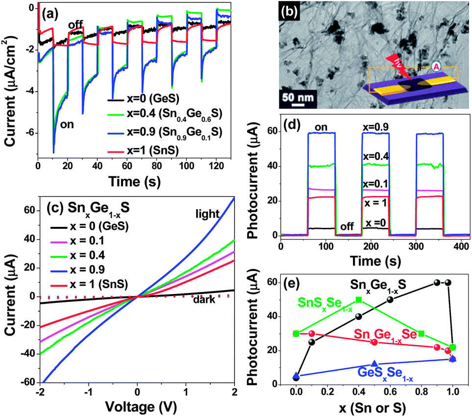 | ||
| Fig. 4 (a) Transient photocurrent of the SnxGe1−xS (x = 0, 0.4, 0.9, and 1) NC film on an ITO substrate in a PEC cell at an applied voltage of −0.5 V under 100 mW cm−2 AM 1.5G illumination, turned on and off at intervals of 10 s. (b) TEM image of the NC–RGO hybrid and a schematic diagram representing the photodetector device. (c) I–V characteristics of SnxGe1−xS (x = 0, 0.1, 0.4, 0.9, and 1) NC–RGO under 514 nm (10 mW) irradiation and in darkness. (d) ΔI–t curves at a bias voltage of 2 V under chopped irradiation. (e) Photocurrents of SnxGe1−xS–, SnxGe1−xSe, SnxGe1−xS–, GeSxSe1−x–, and SnSxSe1−x–RGO as a function of Sn or S content (x). | ||
To gain further insight on their pertinent properties for optoelectronic devices, we also measured the photocurrents of the NCs deposited onto reduced graphene oxide (RGO). Fig. 4b shows the TEM image of the typical 1:1 wt. ratio NC–RGO hybrid nanostructures, which indicates that the NCs are homogeneously anchored onto the RGO nanosheets. The inset shows the schematic diagram of the photodetector fabricated by using the DEP technique. The nanosheet of NC:RGO was deposited between the Ti/Au electrodes separated by a gap of 2 μm onto a silicon oxide substrate.
Fig. 4c shows the current–voltage (I–V) curves of the photodetector composed of SnxGe1−xS–RGO hybrid, under dark conditions and irradiation at 514 nm (2.4 eV) using an Ar ion laser (10 mW). The I–V curves were linear and symmetric within the measured range (−2 to 2 V), indicating good ohmic contact in the device. Upon irradiation, the photocurrents increased linearly with light intensity (2–10 mW). The transient photocurrents (ΔI) at a bias voltage of 2 V were collected with light on/off cycles (Fig. 4d). The photocurrent depended on the composition, distinctively with the higher value of the alloys, as compared with that of their binary counterparts. The much higher photocurrent was observed in the Sn-rich composition. The photosensitivity, defined as the ratio of ΔI to the current under dark conditions, reached a maximum value of 20. In addition, we also measured the photocurrent from the SnxGe1−xSe–RGO photodetectors. As the Sn content (x) increases, the photocurrent decreases rather monotonically with a slight enhancement in the Sn-rich composition. On the other hands, the photocurrent from the anion alloy NC–RGO photodetectors showed the enhancement of alloys for the only SnSxSe1−x–RGO. Fig. 4e shows the photocurrent of the cation and anion alloy NC–RGO photodetectors as a function of x.
Once the excitons are created by the light absorption of the NC, the photoelectrons are directly transferred from their CB (3.6–4.1 eV below the vacuum level) to RGO (work function is 4.5 eV), resulting in a flow toward positive charged electrode. The photogenerated electron–hole pairs separate through the binding between the NC and RGO, creating a large photocurrent. In order to explain the enhancement of photoconversion efficiency of SnxGe1−xS and SnSxSe1−x alloy NCs, we suggest that the SnS composition induces the direct band gap character of the alloy NCs, which may allow more efficient photon absorption and the subsequent generation and separation of electron–hole pairs, thereby increasing photocurrent. We believe that the SnGeS– and SnSSe–RGO hybrid nanostructures prepared in this study hold great promise for use in transparent flexible photodetectors that respond sensitively over the UV-visible-NIR wavelength region.
Conclusion
We report the successful synthesis of composition-tuned SnxGe1−xS, SnxGe1−xSe, GeSxSe1−x, and SnSxSe1−x alloy NCs over the entire compositional range (0 ≤ x ≤ 1) by a facile gas-phase laser photolysis method. The ternary compositions of the NCs were precisely tuned by precise control of the partial pressure of the precursors, namely, TMG, TMT, H2S, and DMS. Four series of the orthorhombic phase alloy NCs prepared in this study covered a wide range of band gaps (0.9–1.6 eV). XRD peak analysis revealed unique anisotropic bowing phenomena of the lattice constants for the cation alloys (SnxGe1−xS and SnxGe1−xSe) NCs. Remarkably, the SnxGe1−xS and SnxGe1−xSe NCs exhibited an optical bowing with a bowing constant of 0.25 and 0.14 eV, respectively, which is correlated with the increase of the lattice parameters. On the other hand, the anion alloy (GeSxSe1−x, and SnSxSe1−x) NCs showed no optical bowing or lattice parameter bowing.Using the UV-visible-NIR spectrum and CV data, we estimated the band-gap position, whose VB and CB locate at 5.0–5.2 eV and 3.6–4.1 eV below the vacuum level, respectively, below the vacuum level. The photodetectors composed of a SnxGe1−xS– and SnSxSe1−x–RGO hybrid showed the significant enhancement of the alloy composition. Based on these results, we suggest that the SnS composition induces the direct band gap character of the alloy NCs. This result provides a benchmark for the alloy effect that has recently attracted much attention in the field of photoconversion devices.
Acknowledgements
This study was supported by NRF (2011-0015235; 2011-0020090; 2011-0013070), WCU (R31-2012-000-10035-0), and KETEP (20104010100640). The HVEM and XPS (Pusan) measurements were performed at the KBSI. The experiments at the PLS were partially supported by MOST and POSTECH.Notes and references
- Y. D. V. Talapin, J. S. Lee, M. V. Kovalenko and E. V. Shevchenko, Chem. Rev., 2010, 110, 389 CrossRef PubMed.
- A. J. Nozik, M. C. Beard, J. M. Luther, M. Law, R. J. Ellingson and J. C. Johnson, Chem. Rev., 2010, 110, 6873 CrossRef CAS PubMed.
- G. Konstantatos and E. H. Sargent, Nat. Nanotechnol., 2010, 5, 391 CrossRef CAS PubMed.
- L. A. Padilha, J. T. Stewart, R. L. Sandberg, W. K. Bae, W.-K. Koh, J. M. Pietryga and V. I. Klimov, Acc. Chem. Res., 2013, 46, 1261 CrossRef CAS PubMed.
- W. Ma, J. M. Luther, H. Zheng, Y. Wu and A. P. Alivisatos, Nano Lett., 2009, 9, 1699 CrossRef CAS PubMed.
- D. K. Smith, J. M. Luther, O. E. Semonin, A. J. Nozik and M. C. Beard, ACS Nano, 2011, 5, 183 CrossRef CAS PubMed.
- J. Akhtar, M. Afzaal, M. Banski, A. Podhorodecki, M. Syperek, J. Misiewicz, U. Bangert, S. J. O. Hardman, D. M. Graham, W. R. Flavell, D. J. Binks, S. Gardonio and P. O’Brien, J. Am. Chem. Soc., 2011, 133, 5602 CrossRef CAS PubMed.
- A. C. Onicha, N. Petchsang, T. H. Kosel and M. Kuno, ACS Nano, 2012, 6, 2833 CrossRef CAS PubMed.
- J. W. Thomson, X. Wang, L. Hoch, D. Faulkner, S. Petrov and G. A. Ozin, J. Mater. Chem., 2012, 22, 5984 RSC.
- A. G. Midgett, J. M. Luther, J. T. Stewart, D. K. Smith, L. A. Padilha, V. I. Klimov, A. J. Nozik and M. C. Beard, Nano Lett., 2013, 13, 3078 CrossRef CAS PubMed.
- Z. Liu, Y. Sun, J. Yuan, H. Wei, X. Huang, L. Han, W. Wang, H. Wang and W. Ma, Adv. Mater., 2013, 25, 5772 CrossRef CAS PubMed.
- I. U. Arachchige and M. G. Kanatzidis, Nano Lett., 2009, 9, 1583 CrossRef CAS PubMed.
- H. Wei, Y. Su, S. Chen, Y. Lin, Z. Yang, H. Sun and Y. Zhang, CrystEngComm, 2011, 13, 6628 RSC.
- R. B. Soriano, C. D. Malliakas, J. Wu and M. G. Kanatzidis, J. Am. Chem. Soc., 2012, 134, 3228 CrossRef CAS PubMed.
- J. He, S. N. Girard, J. C. Zheng, L. Zhao, M. G. Kanatzidis and V. P. Dravid, Adv. Mater., 2012, 24, 4440 CrossRef CAS PubMed.
- H. Wei, Y. Su, S. Chen, Y. Lin, Z. Yang, X. Chen and Y. Zhang, J. Mater. Chem., 2011, 21, 12605 RSC.
- H. S. Im, Y. Myung, Y. J. Cho, C. H. Kim, H. S. Kim, S. H. Back, C. S. Jung, D. M. Jang, Y. R. Lim, J. Park and J. P. Ahn, RSC Adv., 2013, 3, 10349 RSC.
- J. J. Buckley, F. A. Rabuffetti, H. L. Hinton and R. L. Brutchey, Chem. Mater., 2012, 24, 3514 CrossRef CAS.
- Y. Myung, H. S. Im, C. H. Kim, C. S. Jung, Y. J. Cho, D. M. Jang, H. S. Kim, S. H. Back and J. Park, Chem. Commun., 2013, 49, 187 RSC.
- A. M. Elkorashy, J. Phys. C: Solid State Phys., 1988, 21, 2595 CrossRef CAS.
- A. P. Lambros, D. Geraleas and N. A. Economou, J. Phys. Chem. Solids, 1974, 35, 537 CrossRef CAS.
- A. M. Elkorashy, Phys. Status Solidi B, 1986, 135, 707 CrossRef CAS.
- L. Makinistian and E. A. Albanesi, J. Phys.: Condens. Matter, 2007, 19, 186211 CrossRef CAS PubMed.
- A. M. Elkorashy, J. Phys. Chem. Solids, 1986, 47, 497 CrossRef CAS.
- B. Pejova and A. Tanuševski, J. Phys. Chem. C, 2008, 112, 3525 CAS.
- S. M. Yoon, H. J. Song and H. C. Choi, Adv. Mater., 2010, 22, 2164 CrossRef CAS PubMed.
- D. D. Vaughn, II, R. J. Patel, M. A. Hickner and R. E. Schaak, J. Am. Chem. Soc., 2010, 132, 15170 CrossRef PubMed.
- D. J. Xue, J. Tan, J. S. Hu, W. Hu, Y. G. Guo and L. J. Wan, Adv. Mater., 2012, 24, 4528 CrossRef CAS PubMed.
- S. G. Hickey, C. Waurisch, B. Rellinghaus and A. Eychmüller, J. Am. Chem. Soc., 2008, 130, 14978 CrossRef CAS PubMed.
- Y. Wang, H. Gong, B. Fan and G. Hu, J. Phys. Chem. C, 2010, 114, 3256 CAS.
- J. Chao, Z. Xie, X. B. Duan, Y. Dong, Z. Wang, J. Xu, B. Liang, B. Shan, J. Ye, D. Chen and G. Shen, CrystEngComm, 2012, 14, 3163 RSC.
- Z. Deng, D. Cao, J. He, S. Lin, S. M. Lindsay and Y. Liu, ACS Nano, 2012, 6, 6197 CrossRef CAS PubMed.
- J. Chao, Z. Wang, X. Xu, Q. Xiang, W. Song, G. Chen, J. Hu and D. Chen, RSC Adv., 2013, 3, 2746 RSC.
- M. Steichen, R. Djemour, L. Gütay, J. Guillot, S. Siebentritt and P. J. Dale, J. Phys. Chem. C, 2013, 117, 4383 CAS.
- M. A. Franzman, C. W. Schlenker, M. E. Thompson and R. L. Brutchey, J. Am. Chem. Soc., 2010, 132, 4060 CrossRef CAS PubMed.
- W. J. Baumgardner, J. J. Choi, Y. F. Lim and T. Hanrath, J. Am. Chem. Soc., 2010, 132, 9519 CrossRef CAS PubMed.
- S. Liu, X. Guo, M. Li, W. H. Zhang, X. Liu and C. Li, Angew. Chem., Int. Ed., 2011, 50, 12050 CrossRef CAS PubMed.
- K. Jang, I. Y. Lee, J. Xu, J. Choi, J. Jin, J. H. Park, H. J. Kim, G. H. Kim and S. U. Son, Cryst. Growth Des., 2012, 12, 3388–3391 CAS.
- L. Li, Z. Chen, Y. Hu, X. Wang, T. Zhang, W. Chen and Q. Wang, J. Am. Chem. Soc., 2013, 135, 1213 CrossRef CAS PubMed.
- V. H. Krebs and D. Langer, Z. Anorg. Allg. Chem., 1964, 334, 37 CrossRef.
- P. Boudjouk, D. J. Seidler, D. Grier and G. McCarthy, Chem. Mater., 1996, 8, 1189 CrossRef CAS.
- W. H. Zachariasen, Phys. Rev., 1932, 40, 917 CrossRef CAS.
- H. Wiedemeier and H. G. von Schnering, Z. Kristallogr., 1978, 148, 295 CrossRef CAS.
- B. D. Malone and E. Kaxiras, Phys. Rev. B: Condens. Matter Mater. Phys., 2013, 87, 245312 CrossRef.
- R. B. Shalvoy, G. B. Fisher and P. J. Stiles, Phys. Rev. B: Solid State, 1977, 15, 1680 CrossRef CAS.
- C. Y. Fong, W. Weber and J. C. Phillips, Phys. Rev. B: Solid State, 1976, 14, 5387 CrossRef CAS.
- A. Hagfeldt and M. Grätzel, Chem. Rev., 1995, 95, 49 CrossRef CAS.
- M. Parenteau and C. Carolne, Phys. Rev. B: Condens. Matter Mater. Phys., 1990, 41, 5227 CrossRef CAS.
- K. Ramasamy, V. L. Kuznetsov, K. Gopal, M. A. Malik, J. Raftery, P. P. Edwards and P. O’Brien, Chem. Mater., 2013, 25, 266 CrossRef CAS.
- J. E. Bernard and A. Zunger, Phys. Rev. B: Condens. Matter Mater. Phys., 1987, 36, 3199 CrossRef CAS.
- S. H. Wei and A. Zunger, Phys. Rev. B: Condens. Matter Mater. Phys., 1988, 37, 8958 CrossRef CAS.
- S. H. Wei and A. Zunger, Phys. Rev. B: Condens. Matter Mater. Phys., 1997, 55, 13605 CrossRef CAS.
- S. H. Wei, S. B. Zhang and A. Zunger, J. Appl. Phys., 2000, 87, 1304 CrossRef CAS.
- J. C. Wu, J. Zheng, C. L. Zacherl, P. Wu, Z. K. Liu and R. Xu, J. Phys. Chem. C, 2011, 115, 19741 CAS.
- M. Sugiyama, K. T. R. Reddy, N. Revathi, Y. Shimamoto and Y. Murata, Thin Solid Films, 2011, 519, 7429 CrossRef CAS.
- Y. H. Li, A. Walsh, S. Chen, W. J. Yin, J. H. Yang, J. Li, J. L. F. Da Silva and S. H. Wei, Appl. Phys. Lett., 2009, 94, 212109 CrossRef.
Footnote |
| † Electronic supplementary information (ESI) available: Tables S1–S3, Fig. S1–S7. XRD pattern, EDX data, Raman spectrum, Kubelka–Munk transformation data of UV-visible-NIR absorption spectrum, and CV curves. See DOI: 10.1039/c4ra01011f |
| This journal is © The Royal Society of Chemistry 2014 |