 Open Access Article
 This Open Access Article is licensed under a
 Creative Commons Attribution 3.0 Unported Licence
Au-NR/VO2-NP nanocomposites supported on glass substrates: microstructure and optical properties†
Salah
Habouti
and
Mohammed
Es-Souni
*
Institute for Materials & Surface Technology (IMST), 24149 UAP Kiel, Germany. E-mail: me@fh-kiel.de; Fax: +49 431 210 2660; Tel: +49 431 210 2660
First published on 7th January 2014
Abstract
On-glass-substrate gold nanorods (Au-NRs) are processed via electrodeposition into anodized alumina template films that were fabricated using an Al/Au/Ti film stack on glass. The Au-NRs are capped with VO2 nanoparticles obtained from sputtered vanadium caps. The nanostructure arrays show intense plasmon resonance and are thermochromic with VO2 size dependent transition temperature.
Composites of oxide nanoparticles (NPs), mostly semi-conductor oxides and noble metal nanostructures, are the focus of intense research activities because they show promising light harvesting properties for applications spanning the range from dye sensitized solar cells, to water splitting, to photocatalysis.1,2 The improved light absorption in the main solar spectrum range of these nanocomposites – that is at the origin of their superior properties – is mediated by the localized surface plasmon resonance of the noble metal nanoparticles.1,2 However, with the exception of the recent work by the group of Moskovits,2 where supported Au-nanorods were used as a plasmonic substrate, research is mostly focused on colloidal NPs and films limiting practical use in the case of the former and available active surface for the latter.
Supported discrete nanocomposites are most propitious to control both surface area and structure dimensions which in turn allow the tuning and control of the absorption range.
In the present paper, we report on the fabrication of supported Au-nanorods (NRs) using thin porous alumina films (PAF) on glass substrates that were subsequently capped with VO2-NPs. These nanocomposites present unusual optical properties as they combine plasmonic absorption with thermochromism. Reports on on-substrate 1D noble metal nanostructures using supported PAF are scarce,4 among them our own work,5 and a recent study on supported Au-NR/TiO2 nanocomposites for water splitting.2 Notwithstanding their somewhat laborious processing, supported plasmonic structures have substantial advantages over nanostructures processed via freestanding PA membranes, because they are easy to handle and can be better scaled-up for device applications as a variety of substrates, including technologically important ones such as ITO glass and polymers, may be used.
The experimental procedure is described in detail in the ESI and Fig. 1s† schematically describes the fabrication steps of the AAO films and Au-NR electrodeposition.
SEM micrographs of the PAF template as well as the Au-NR array are shown in Fig. 1. The electrolyte used here leads to corrugated NRs with furrow-like appearance. Their distribution is homogeneous (see Fig. 2s†) with a mean spacing of 50 nm, a mean diameter of 70 nm and a mean length of 300 nm.
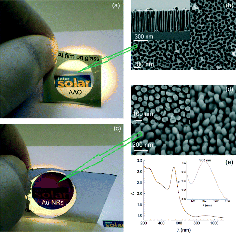 | ||
| Fig. 1 (a) Photograph showing the transparent PAF on glass (surrounding it is the non-anodized Al-film); (b) SEM micrograph of the PAF template, top view and cross-section (inset); (c) photograph of the electrodeposited Au-NR after removal of PAF; (d) SEM micrograph of the Au-NRs: tilted and top (inset) views; (e) UV-Vis optical absorption properties showing two plasmonic peaks (see text for discussion). | ||
The extinction spectrum of these NRs is also displayed in Fig. 1 and shows a sharp and intense absorption maximum at 540 nm and a broad weak absorption peak centred around 900 nm. These peaks arise from the anisotropy of the Au-NRs that lead to the splitting of dipole plasmon resonance into transverse (540 nm) and longitudinal (900 nm) modes.5,6 Their loci are known to be dependent on dimensions (diameter and length), spacing and dielectric environment of the NRs.6
Fig. 2a shows the Au-NRs after sputtering 10 nm of elemental vanadium. The vanadium layer condenses primarily on the NR tips forming caps (5 nm V on NRs could not be resolved). The nature of the interface between Au and V is not known, but the Au–V phase diagram,7 both in the V- and in the Au-rich region, shows the formation of solid solutions with eventually the presence of intermetallic phases depending on composition and temperature. Hence, we may expect intermixing between V and Au at the interface at least for a few atomic layers upon sputtering. After heat treatment (Fig. 2b and c), VO2 (see below for phase analysis) grows on top of the Au-NRs and either forms NPs (in the case of 5 nm V) (Fig. 2b (see also Fig. 2s†)) or grows vertically, forming NRs consisting of stacks of nanosheets that are well visible in Fig. 2c. Some of the VO2 nanostructures in Fig. 2c merge laterally but the majority of them grow vertically, forming discrete structures on the Au-NRs.
 | ||
| Fig. 2 (a) SEM micrograph of vanadium capped Au-NRs obtained by sputter deposition of 10 nm vanadium. The caps are clearly seen on top of the Au-NRs (arrows); (b) SEM micrograph of VO2-NPs (arrows) on top of Au-NRs obtained after annealing 5 nm sputtered vanadium; (c) VO2-NPs and NRs obtained from 10 nm sputtered vanadium and growing vertically on Au-NRs. | ||
Structural analysis using XRD was not conclusive as only very weak and broad peaks of VO2 could be obtained from grazing incidence patterns of the 10 nm film (V thickness) (Fig. 3s†). In contrast, Raman scattering demonstrates unambiguously the presence of characteristic vibrations of VO2 that are very well resolved down to 5 nm (vanadium thickness) (Fig. 3) even at the lowest laser power of 0.2 mW that is necessary in order to prevent oxidation of VO2 to V2O5 during measurement.
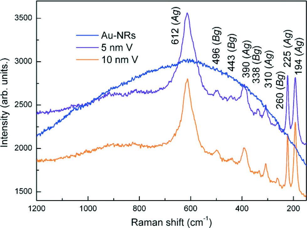 | ||
| Fig. 3 Raman scattering spectra showing the characteristic vibrations of VO2 (ref. 8) obtained from VO2-NPs on Au-NRs corresponding to Fig. 2b and c. The VO2-NPs were obtained after annealing 5 and 10 nm of sputtered vanadium on Au-NRs. The fluorescence spectrum of the Au-NRs is also shown. | ||
The observation of tiny amounts of VO2@Au-NRs using Raman scattering with the relatively high band intensities shown in Fig. 3 is a direct consequence of surface enhanced Raman scattering (SERS) that is a very well-known method for the analysis of trace amounts of different substances, and is based on electromagnetic field enhancement by the plasmonic structure.9 Most of the published studies, however, are on dyes and other organic molecules, including DNA, as well as viruses.10 The only work on SERS of oxides is by Donev et al. who reported on Au-capped VO2 particles of 120 nm that were fabricated by pulsed laser deposition and lithographic techniques (in their work, Au was placed on VO2).3
The present study shows that supported Au-NRs may constitute powerful substrates for the detection of inorganic NPs, in addition to their high enhancement factor shown in earlier work for organic molecules.5 Moreover, as mentioned above, they can also be advantageously used as an active support for other functional nanomaterials, among them VO2 that constitutes a highly interesting multifunctional material. VO2 is a well-known thermochromic material that undergoes a reversible semiconductor–metal phase transition (SMT) at 68 °C from a low temperature monoclinic (P21/c) to a metallic tetragonal phase (P42/mnm) with a rutile structure (VO2 (R)).11 The metallic phase exhibits high reflectance in the IR range without trade-off of transmittance in the visible region that makes VO2 promising for smart window applications. The main benefit lies in minimizing energy consumption for air conditioning of buildings without all too strongly impairing visible light transmission.12 However, one serious hindrance for industrial application is the high transition temperature which, for higher efficiency, must be lowered to below 40 °C. Doping with Mo and W was shown to decrease the SMT temperature in discrete nanostructures to room temperature, depending on doping concentration (see the review by Whittaker et al.13). Scaling VO2 down to nanosize dimensions can also affect the SMT characteristics, with the transition temperature being strongly correlated to clamping and stress effects from the substrate.
The UV-Vis-transmittance properties of the VO2@Au-NR structure at different temperatures are shown in Fig. 4a. The minimum at 540 nm for the bare Au-NRs is red-shifted to 565 nm for VO2-NPs@Au-NRs that can be explained by the different dielectric environments arising from the presence of VO2, a well-known effect on plasmonic structures.14 At the onset of SMT at 60 °C (see below), a small red-shift of 4 to 6 nm is also observed due to the structural change. The weak longitudinal plasmonic peak at 900 nm is strongly attenuated by the presence of VO2-NPs. With increasing temperature, the transmittance decreases in the near IR region and substantially between 60 and 70 °C, owing to SMT. This behaviour is reversible with the formation of a hysteresis (Fig. 4b), characteristic for this type of martensitic transformation, because the reversible phase transformation is limited by nucleation and growth. The VO2-NPs derived from the 10 nm thick vanadium film show a somewhat broad hysteresis loop with a forward transformation temperature of approximately 60 °C and a backward temperature of 45 °C. In contrast, a shallower hysteresis loop is obtained from the 5 nm thick vanadium film with transformation temperatures of approximately 45 and 40 °C for the forward and backward transformation, respectively (Fig. 4s†).
 | ||
| Fig. 4 (a) UV-Vis transmission spectra of VO2-NPs@Au-NRs at different temperatures. The transmission minimum corresponds to the transverse plasmonic mode of Au-NRs in the presence of VO2 NPs. The decrease in transmittance in the near IR region results from the semiconductor–metal transition of VO2. (b) Forward and backward transmittance as a function of temperature at a wavelength of 1100 nm for 10 nm VO2 on Au-NRs. The inset shows the derivative of the hysteresis loop to determine the phase transition temperature. | ||
The values obtained for the SMT temperature largely differ from that of bulk VO2. This might be regarded as the consequence of two correlated effects: the nanoscale dimension of the VO2-particles and the electron injection from the Au-NRs. The VO2–Au interface is a semiconductor–metal heterojunction involving different work functions (5.4 eV for VO2 (ref. 15) and 4.8 eV for Au with respect to the vacuum level). Electrons are expected to flow through the junction from Au leading to band-bending (valence and conduction band) of VO2 toward the metal junction and alignment of the Fermi levels. This is schematically depicted in Fig. 5s.† It is thought that the increase of electron concentration in the semi-conducting phase leads to its destabilization, thus lowering the energy barrier of the transformation into the metallic phase. This mechanism is rather in favor of the Mott–Hubbard transition,11 already put forward for the lowering of the SMT temperature in epitaxial VO2 thin films covered with Au-NPs.16 The occurrence of plasmon electrons is a prerequisite for lowering the SMT transition temperature, as we have shown in previous work that the presence of VO2 on large Au-clusters did not result in any SMT shift.17
The 5 nm vanadium film yields mostly single VO2-nanoplatelets of 20 to 50 nm diameter on top of the Au-NRs, and may explain the lower SMT temperature obtained here. In contrast, the 10 nm film results in larger VO2 structures that are made of VO2 nanoplatelet stacks, as mentioned above and shown in Fig. 2c. In this case, the effect of the Au–VO2 interface on the SMT temperature is thought to be mitigated by the more sluggish transformation away from the interface, i.e. along the platelet stack. There are, however, additional effects that should also contribute to the lowering of the SMT temperature. For instance, interfacial stresses and stresses arising from SMT that could hinder phase transformation might be considered minimal because the VO2-NPs are supported on self-standing Au-NRs that imply low hydrostatic stresses, provided that nucleation and growth are from surface sites.13
In summary, a novel on-glass-substrate supported nanostructure array consisting of VO2 capped Au-NRs was presented. The processing method can be extended to other noble metals and functional oxide nanostructures and is easily scalable to larger area structures. The particular structure reported here combines localized surface plasmon resonance through Au-NRs and thermochromic properties via VO2-NPs. The thermochromic properties of the structure, demonstrated via temperature dependent transmission measurements, are largely size dependent with a semiconductor–metal transition temperature of roughly 40 °C for VO2-NPs in the size range from 20 to 50 nm.
Notes and references
- Y. Tian and T. Tatsuma, J. Am. Chem. Soc., 2005, 127, 7632–7637 CrossRef CAS PubMed; Y. Nishijima, K. Ueno, Y. Yokota, K. Murakoshi and H. Misawa, J. Phys. Chem. Lett., 2010, 1, 2031 CrossRef; A. Tanaka, S. Sakaguchi, K. Hashimoto and H. Kominami, ACS Catal., 2013, 3, 79 CrossRef.
- J. Lee, S. Mubeen, X. Ji, G. D. Stucky and M. Moskovits, Nano Lett., 2012, 12, 5014–5019 CrossRef CAS PubMed; S. Mubeen, J. Lee, N. Singh, S. Krämer, G. D. Stucky and M. Moskovits, Nat. Nanotechnol., 2013, 8, 247 CrossRef PubMed.
- E. U. Donev, J. I. Ziegler, R. F. Haglund Jr. and L. C. Feldman, J. Opt. A: Pure Appl. Opt., 2009, 11, 125002 CrossRef.
- G. A. Wurtz, P. R. Evans, W. Hendren, R. Atkinson, W. Dickson, R. J. Pollard and A. V. Zayats, Nano Lett., 2007, 7, 1297 CrossRef CAS PubMed; S. Mátéfi-Tempfli and M. Mátéfi-Tempfli, Adv. Mater., 2009, 2, 4005 CrossRef.
- S. Habouti, M. Mátéfi-Tempfli, C.-H. Solterbeck, M. Es-Souni, S. Mátéfi-Tempfli and M. Es-Souni, Nano Today, 2011, 6, 12 CrossRef CAS PubMed; S. Habouti, M. Mátéfi-Tempfli, C.-H. Solterbeck, M. Es-Souni, S. Mátéfi-Tempfli and M. Es-Souni, J. Mater. Chem., 2011, 21, 6269 RSC.
- S. Link, M. B. Mohamed and M. A. El-Sayed, J. Phys. Chem. B, 1999, 103, 3073 CrossRef CAS; J.-W. Kim, E. I. Galanzha, V. Shashkov, H.-M. Moon and V. P. Zharov, Nat. Nanotechnol., 2009, 4, 688 CrossRef PubMed.
- J. F. Smith, Bull. Alloy Phase Diagrams, 1981, 2, 344 CrossRef.
- P. Schilbe, Phys. B, 2002, 316, 600 CrossRef.
- S. Lal, N. K. Grady, J. Kundu, C. S. Levin, J. B. Lassiter and N. J. Halas, Chem. Soc. Rev., 2008, 37, 898 RSC.
- J. Kneipp, H. Kneipp and K. Kneipp, Chem. Soc. Rev., 2008, 37, 1052 RSC.
- A. Zylberstejn and N. F. Mott, Phys. Rev. B: Solid State, 1975, 11, 4383 CrossRef.
- Z. Zhang, Y. Gao, H. Luo, L. Kang, Z. Chen, J. Du, M. Kanehira, Y. Zhang and Z. L. Wang, Energy Environ. Sci., 2011, 4, 4290 CAS.
- L. Whittaker, C. J. Patridge and S. Banerjee, J. Phys. Chem. Lett., 2011, 2, 745 CrossRef CAS.
- K. M. Mayer and J. H. Hafner, Chem. Rev., 2011, 111, 3828 CrossRef CAS PubMed.
- A. I. Gavrilyuk, T. G. Lanskaya, A. A. Mansurov and F. A. Chudnovskii, Sov. Phys. Solid State, 1984, 26, 117 Search PubMed.
- G. Xu, C.-M. Huang, M. Tasawa, P. Jin, D.-M. Chen and L. Miao, Appl. Phys. Lett., 2008, 93, 61911 CrossRef PubMed.
- R. Minch and M. Es-Souni, CrystEngComm, 2013, 15, 6645 RSC.
Footnote |
| † Electronic supplementary information (ESI) available: Materials and methods: processing of PAF template films on glass substrates; processing of Au-NRs and VO2 capped Au-NRs; characterization methods; Fig. 1s–5s. See DOI: 10.1039/c3ce42097c |
| This journal is © The Royal Society of Chemistry 2014 |