
 Open Access Article
 This Open Access Article is licensed under a
 Creative Commons Attribution 3.0 Unported Licence
Theoretical study of electronic structure, lone pair localization, and electronic transport properties of unconventional bulk and 2D γ-SnSe and γ-SnS†
Nguyen Truong Long *a,
Huynh Anh Huya,
Neeraj Mishrabc and
Guy Makovb
*a,
Huynh Anh Huya,
Neeraj Mishrabc and
Guy Makovb
aSchool of Physics Education, Can Tho University, Can Tho 900000, Vietnam. E-mail: truonglong@ctu.edu.vn
bDept. of Materials Engineering, Ben-Gurion University of the Negev, Beer Sheva 84105, Israel
cDepartment of Chemical and Materials Engineering, University of Alberta, Edmonton, AB T6G2V4, Canada
First published on 16th May 2025
Abstract
Tin-based monochalcogenides, particularly SnSe and SnS, are of growing interest due to their cost-effectiveness, environmental compatibility, and exceptional thermoelectric properties. Beyond the conventional α-Pnma phase, these materials can adopt alternative bulk and low-dimensional structures with distinct electronic and transport characteristics. The recent experimental discovery of a layered γ-Pnma SnSe phase in 2023 has further stimulated the search for novel structural allotropes within this family and the assessment of their electronic properties. In this study, we employ density functional theory to examine the structural stability, electronic structure, lone-pair characteristics, and thermoelectric performance of γ-SnS and γ-SnSe in both bulk and two-dimensional (2D) monolayer forms. Our results demonstrate that γ-SnSe and γ-SnS monolayers are thermodynamically stable and can be synthesized via mechanical exfoliation. Electronic structure analysis reveals a substantial band gap expansion in the 2D monolayers, increasing by a factor of 4 to 20 compared to the bulk. A detailed investigation of localized lone pairs in the 2D monolayers identifies two distinct p-state contribution schemes for γ- and α-monolayers, with a notable involvement of the Sn 5p state. Additionally, both bulk and monolayer γ-SnSe and γ-SnS exhibit large Seebeck coefficients and power factors, comparable to or exceeding those of the conventional α-Pnma phases.
1 Introduction
In recent years, tin monochalcogenides, such as SnS and SnSe, have attracted significant research interest as functional materials for optoelectronic and thermoelectric applications.1–4 The discovery of an extraordinary thermoelectric figure of merit (ZT > 2) in conventional α-Pnma SnSe,5 together with the promising thermoelectric properties of related monochalcogenides, including SnS, SnTe, PbS, and PbTe (ZT of 1.05, 1.46, 1.51, and 1.59, respectively) makes them candidate thermoelectric materials.6 Notably, SnS and SnSe are economical, low toxic, and earth-abundant, so they are attractive functional materials for photovoltaic and thermoelectric applications in comparison with the current materials.3 Beyond their thermoelectric applications, SnS and SnSe compounds exhibit attractive electronic and optical properties for extensive applications in optoelectronic and photovoltaic devices.7–11The conventional structure of SnSe and SnS is space group Pnma (Z = 62), denoted as α-phase, is a layered crystal and possesses an indirect bandgap of 0.9–1.0 eV.12,13 They have potential utility as an absorber material in solar cells due to its high absorption coefficient and high hole mobility.7 Especially, α-SnSe has excellent thermoelectric conversion ability, with a figure of merit of ∼2.6 at 923 K, due to its low thermal conductivity and high power factor.11,14 Therefore, SnSe crystals are currently being developed as an economical alternative with superior performance for commercial thermoelectric cooling, along with several high potential thermoelectric materials such as highly disordered or layered compounds Cu2−xS, Cu2−xSe, AgSbSe2, In4Se3, and CsAg5Te3 (ref. 15 and 16) to replace the present Bi2Te3-based alloy.3,17 Recently, two unconventional metastable phases of SnS and SnSe, namely layered γ-SnSe and cubic π-SnSe/SnS, have been discovered experimentally and possess semiconductor gaps varying from ultranarrow band gap of 0.095 eV in γ-Pnma SnSe18,19 to wider band gaps of 1.53/1.28 eV in π-cubic SnS/SnSe,20,21 respectively. These novel allotropes of SnSe and SnS exhibit a range of versatile properties, such as small electron effective mass, low thermal conductivity, and high optical absorption coefficients similar to conventional α-structure.17 Furthermore, the unconventional phases can enable band gap selection, exhibit anisotropy, and facilitate unique nanoscale morphologies such as nano-size particles or low-dimensional structures.
Since SnS and SnSe phases exhibit layered structures, it is possible to form two-dimensional (2D) monolayers experimentally by exfoliation or Li-intercalation.22–25 Among the 2D layered materials, 2D α-SnS and α-SnSe have been extensively explored for electronic structure, mechanical properties, and versatile applications in thermoelectric and optoelectronics10,26–30 In particular, remarkable thermoelectric properties have been reported for the conventional 2D α-monolayer SnS and SnSe relative to 3D bulk phase, demonstrating their high power factor and considerable ZT values.2,29,30 2D monolayers of SnS and SnSe could maintain high stability, high power factor, and low lattice thermal conductivity.30 This leads to estimated ZT values of nearly 0.8 for 2D α-SnS and 2D α-SnSe at 900 K.30 Thus, 2D monolayers of SnS and SnSe are considered mid-temperature thermoelectric materials.2
Aside from the conventional α-structure SnS and SnSe in 2D and bulk phases, several novel unconventional 3D and 2D structures of SnSe have been discovered or predicted to expand the potential applications of this family in optoelectronic and energy conversion devices.13,31–34 It is interesting to examine the thermoelectric transport characteristics of unconventional bulk and 2D structures, such as the newfound γ-phase of SnSe and SnS, as they could possess similar or better properties than the conventional α-structure. In addition, exploring new structures helps develop our fundamental understanding of the electronic and transport characteristics of this family of thermoelectric functional materials, e.g. ref. 13. Particularly, the presence of stereochemically active lone pairs in SnS and SnSe induces the manifestation of multiple polymorphs from the symmetric rock salt structure. Therefore, the diversity of lone pair presence could be a major avenue to understanding the electronic structure and interatomic bonding in SnS and SnSe, which leads to enhanced thermoelectric properties. Motivated by the recent development of low-dimensional structures of SnS and SnSe, our study focuses on two-dimensional structures of γ-SnS and γ-SnSe based on the synthesized novel bulk phase.19 We explore the electronic and electronic transport properties of 2D γ-SnS and γ-SnSe to evaluate their potential application in thermoelectric devices. We also compare the electronic structures, presence of lone pair, and electronic transport properties between the 3D and 2D structures of γ-phase to provide an extensive evaluation of this unconventional structure.
2 Calculation methods
We performed DFT calculations with a plane wave basis set using the Quantum Espresso suite of software.35 Our DFT calculation employed ultrasoft pseudopotentials36 from PS library37 based on generalized gradient approximation (GGA) by the Perdew–Burke–Ernzerhof (PBE) exchange-correlation functional.38 In addition, we utilized the hybrid functionals PBE0(ref. 39) to improve the accuracy of electronic structure and included van der Waals (vdW) interactions based on nonlocal correlation functional vdW-DF3-opt1.40,41 The pseudopotentials accommodate fourteen valence electrons of Sn (4d103s23p2) and six valence electrons of S (3s23p4) and Se (4s24p4). To obtain the optimized structure of monolayers for both α- and γ-structures of SnS and SnSe, we used variable-cell relaxation conditions at a cutoff energy of 60 Ry to achieve reasonably converged energy and calculation cost. The convergence threshold for the self-consistent field calculations is at 10−8 eV, and the optimal force condition for variable-cell relaxation is 10−4 eV Å−1. Our calculations utilize Monkhorst–Pack k-grid42 of 8 × 8 × 8 k-points for 3D structure and 16 × 16 × 1 for 2D structure. For the 2D structure, we added a vacuum space of 20 Å to eliminate the effect of periodic images. The dynamical stability of our 2D monolayer phases of SnS and SnSe was evaluated by calculating the phonon dispersion curves using density functional perturbation theory43 with grids of 12 × 12 × 1 in k-space and a 3 × 3 × 1 q-mesh. The electronic structure and the projected density of states (PDOS) were calculated for the final optimized structures. Interpretation of crystal orbital Hamilton population (COHP)44 is applied to investigate the lone pairs in each monolayer structure. The energy range corresponded to lone pairs in the COHP analysis is used to calculate the integrated density of states (IDOS) for each contributor orbitals to the lone pairs. Electronic transport properties of 2D SnS and SnSe structures, including Seebeck coefficient and electrical conductivity, were calculated using semi-classical Boltzmann transport theory as developed in BoltzTraP2,45 widely applied by various DFT calculations for thermoelectric research. We employed BoltzTraP2 under two approximations of the rigid band and constant electron relaxation time, τ, (CRTA). Transport properties such as electrical conductivity (σ), Seebeck coefficient (S), and power factor (PF = S2σ) are determined as a function of the chemical potential, μ, and temperature, following other studies of thermoelectric materials.46–48 The Boltzmann's transport equation for electrical conductivity and Seebeck coefficient are described in BoltzTrap2(ref. 45) as follows:Transport distribution function:
 | (1) |
Electrical conductivity:
 | (2) |
Seebeck coefficient:
 | (3) |
 is the group velocity, τi,k is the relaxation time, f(ε;μ,T) is the Fermi distribution function,
  is the electron density of states, and
  is the effective carrier density.
In this study, the electrical conductivity, and thus the power factor, is estimated as the relative electrical conductivity σ/τ (τ is the relaxation time) and relative power factor, PF = σ2S/τ. The electron relaxation time τ cannot be calculated directly in our current work and is usually approximated by a typical value τ = 10−14 s,45 or obtained from fitting the experimental data. Such experimental data is not available yet for the γ-phase and its monolayer. For the calculation of transport properties, we employed a dense k-point sampling of 24 × 24 × 1.
3 Results and discussion
3.1 Crystal structure of monolayer and bulk phases of γ-SnS and γ-SnSe
The lattice parameters and bond lengths of 2D and 3D γ-SnS and γ-SnSe, compared to their conventional 3D α-Pnma counterparts, were calculated and summarized in Table 1. The 2D monolayers of α- and γ-phase of SnS and SnSe are arranged in different hierarchies of the same space group Pmn21 (Z = 31), as illustrated in Fig. 1. The basic structure of all four phases of SnS and SnSe is a tetrahedron comprising one Sn atom bonded to three chalcogen atoms. While the atomic arrangement of conventional α-SnS and SnSe resemble black phosphorus, γ-SnS and γ-SnSe present a relatively small out-of-plane atomic distortion. We found that lattice parameters of 2D structures of SnS and SnSe are close to their bulk values, within a maximum difference of 0.25 Å.| Structure | Formation energy ΔEf (meV per atom) | 2D surface energy (meV Å−2) | a (Å) | b (Å) | c (Å) | Layer thickness h | Short bond (Å) | Long bond (Å) |
|---|---|---|---|---|---|---|---|---|
| Bulk α-SnS | 0 | — | 4.02 | 4.31 | 11.26 | 2.939 | 2.66 | 2.69 |
| Bulk γ-SnS | 6.46 | — | 4.01 | 5.98 | 8.47 | 2.216 | 2.67 | 2.70 |
| 2D α-SnS | 147.9 | 17.6 | 4.08 | 4.31 | — | 2.846 | 2.59 | 2.74 |
| 2D γ-SnS | 158.4 | 14.8 | 3.80 | 5.87 | — | 2.199 | 2.61 | 2.76 |
| Bulk α-SnSe | 0 | — | 4.21 | 4.56 | 11.78 | 3.034 | 2.78 | 2.83 |
| Bulk γ-SnSe | 2.99 | — | 4.19 | 6.23 | 8.56 | 2.328 | 2.80 | 2.84 |
| 2D α-SnSe | 165.5 | 17.9 | 4.28 | 4.41 | — | 2.756 | 2.73 | 2.90 |
| 2D γ-SnSe | 197.6 | 16.8 | 3.94 | 6.19 | — | 2.002 | 2.74 | 2.94 |
 | ||
| Fig. 1 Structures of 3D bulk and 2D monolayers of α- and γ-SnS and SnSe (blue: Sn and yellow: S or Se). (a) Bulk 3D α-structure of SnS and SnSe. (b) Bulk 3D γ-structure of SnS and SnSe. (c) Monolayer 2D α-structure of SnS and SnSe (top and side view). (d) Monolayer 2D γ-structure of SnS and SnSe (top and side view). | ||
In more detail, the bonding of Sn with chalcogen atoms in a single layer can be classified into two bond types, denoted as the short and long bonds, as shown in Fig. 1c and d. The Sn–S and Sn–Se bond lengths in the α- and γ-structures show slight variations. In the γ-phase, the longer bonds are relatively larger than those in the α-phase, in both 2D and 3D lattices (see Fig. 1). Sn–Se bonds are longer than Sn–S in all cases. The short bond in the 2D structure is shortened while the long bond is elongated compared to their 3D counterparts (see Table 1). The stronger short bond in the 2D structure indicates the increased out-of-plane interaction with respect to the 2D/layer plane, and the stretched long bond represents the weaker in-plane interaction, as seen in Fig. 1. To characterize the distortion of a single layer in both 3D and 2D structures of α- and γ-phases, we calculate its thickness, h, as the separation between two layers of Sn atoms, as shown in Fig. 1. We find that the thickness h of both 2D monolayers is smaller than the layer thickness in their bulk counterparts.
To compare the energetic stability of 2D and 3D layered structures, we calculated the relative formation energy difference per atom, ΔEf, for all considered phases of SnS and SnSe with respect to the ground states of bulk α-SnS and α-SnSe as reference values. The equation of the formation energy differences ΔEf is expressed as follows:
 | (4) |
 | (5) |
To further evaluate the possible synthesis of 2D phases of γ-SnS and γ-SnSe, we estimate the feasibility of the mechanical exfoliation process to obtain a monolayer structure. Theoretically, the mechanical exfoliation must overcome cleavage energy determined by the interlayer coupling strength between two layers. The cleavage energy can be estimated by employing the extraction of one layer from a supercell containing several layers, as shown in Fig. 2, separated by distance d with respect to the interlayer separation d0 in the bulk configuration, considered an efficient method for obtaining monolayer 2D materials.27,33,52,53 Therefore, we evaluate the cleavage energy required to extract one layer of γ-SnS and γ-SnSe from the bulk phase. The cleavage energy presents a gradual increment with the difference distance (d − d0) and converges to a fixed value at approximately 8 Å. Our calculated cleavage energies by mechanical exfoliation of 2D γ-SnS and γ-SnSe converge to values of 0.69 J m−2 and 0.71 J m−2, respectively, comparable to previous calculations of similar monolayer SnSe,33,52 noting that ref. 52 denoted our structure as β-SnSe. The cleavage energy of 2D γ-SnSe is slightly lower than 2D γ-SnS, as seen in Fig. 2. Both cleavage energies of 2D γ-SnS and γ-SnSe are higher than those of pure elemental monolayers such as graphene (0.32–0.37 J m−2), phosphorene (0.37 J m−2),25,31,50 and only slightly higher than the cleavage energies of 2D α-SnSe (0.48 J m−2)27 and α-GeS (0.52 J m−2).53 These cleavage energies of γ-SnS and γ-SnSe are considerably lower than in other 2D materials, as GeP3 (0.91–1.14 J m−2), Ga2N (1.09 J m−2), and InP3 (1.32 J m−2).33,52 Our results for the surface energy and cleavage energy suggest that the exfoliation of 2D γ-SnS and γ-SnSe from 3D bulk is energetically feasible. However, the high cleavage energy for 2D γ-SnS and γ-SnSe at 0.69 J m−2 and 0.71 J m−2 predicts difficulty for mechanical exfoliation. We suggest using alternative methods, such as liquid-phase exfoliation or chemical intercalation, to synthesize 2D γ-SnS and γ-SnSe. The close value of cleavage energy hints that similar exfoliation techniques of 2D α-phase could be applied to the recently synthesized bulk phase of γ-SnSe.19
 | ||
| Fig. 2 Cleavage energy in J m−2 for mechanical exfoliation of γ-structures of SnS and SnSe from 3D bulk phase. | ||
We calculated the phonon dispersion relations for 2D α- and γ-structures of SnS and SnSe as shown in Fig. 3. The positive frequencies obtained across the reciprocal space confirm the dynamical stability of these structures. The phonon spectra for the 2D structures contain a new parabolic branch near the Gamma point, typical of 2D structures, that replaces the third acoustic branch in the 3D structure. Phonon dispersions of 2D SnS and SnSe do not express a phononic band gap, in contrast to the bulk phases of SnSe and SnS, which possess phononic band gaps of 0.7–2 THz in the optical phonon spectrum.13 Fig. 3 illustrates that the optical phononic frequencies of 2D SnSe are lower than 2D SnS in both monolayer allotropes. This point is interesting as the absence of phononic band gap in our 2D structures is probably preferred for thermoelectric materials. The phononic band gap could result in higher thermal conductivity due to the longer mean free path of acoustic-optical phonon scattering.54–56 Bulk α-SnSe possesses ultralow lattice thermal conductivity at around 0.64 W m−1 K−1 at 300 K and decreases to 0.45 W m−1 K−1 at 973 K, which is highly desirable in the search for high thermoelectric performance.14,15 In addition, materials without a phononic band gap and attaining rattling modes in low-energy phonons could also provide low thermal conductivity.16 Hence, the phonon calculation hints that our 2D structures are not only dynamically stable, but could also be favorable candidates for thermoelectric applications.
 | ||
| Fig. 3 Phonon dispersion curves of 2D α and γ monolayers of SnS and SnSe. | ||
 | ||
| Fig. 4 (a) Band structures of α and γ-SnS. (b). Band structures of α and γ-SnSe. | ||
| Structure | α-SnS | γ-SnS | Bandgap (eV) | α-SnSe | γ-SnSe |
|---|---|---|---|---|---|
| 2D monolayer bandgap (eV) | 1.66 | 1.76 | 2D monolayer | 1.05 | 1.86 |
| 1.83,61 1.56,30 1.58,57 1.82 (ref. 58) | — | 1.4,25 0.89,30 0.71,61 0.65,59 0.86 (ref. 24) | 1.52,32 2.25 (ref. 33) | ||
| CBM | Adjacent X | Between X–Γ | CBM | Adjacent X | Between Y–Γ |
| VBM | Adjacent Y | Between X–Γ | VBM | Adjacent Y | Between X–Γ |
| 3D bulk bandgap (eV) | 1.03 | 0.40 | 3D bulk | 0.93 | 0.097 |
| 1.1,60 1.2–1.37 (ref. 58 and 62) | 0.45,13 0.59 (ref. 63) | 0.89–0.93,7,58,60 1.00 (ref. 62) | 0.095 (ref. 19) | ||
| CBM | Between X–Γ | S | CBM | Adjacent Y | U |
| VBM | Y | Between X–Γ | VBM | Adjacent Z | Between X–Γ |
We calculated the PDOS of α and γ structures in both 3D bulk and 2D monolayer of SnS and SnSe, which are presented in Fig. 5. The overall hybridization of Sn–S and Sn–Se orbitals follows the same scheme in 2D and 3D. The conducting bands just above the Fermi level of α and γ structures are dominated by Sn 5p states with a considerable contribution from chalcogen's p-states. The valence bands below consist mainly of chalcogen's p-states mixed with the Sn 5s and 5p states (see Fig. 5). This hybridization between mixed Sn s–p states with the p-states of the chalcogen in the valence band results in the formation of stereo-active lone pairs.12,13,64 A previous study13 of metastable phases of SnS and SnSe suggested that the variations in the contributions of the three p-orbitals of chalcogen atoms to the lone-pair led to a wide variety of layered SnS and SnSe structures. In this study, we provide a comparison of 2D and 3D allotropes of α and γ phases of SnS and SnSe (see Fig. 5) and consequently interpret the electronic localized function (ELF) in Fig. 6 to indicate the distinctness of the 2D phase.
 | ||
| Fig. 5 PDOS of 2D monolayer compared to 3D bulk of α and γ structures of SnS and SnSe. | ||
 | ||
| Fig. 6 Visualization of lone pairs of 2D and 3D allotropes of α and γ phases of SnS and SnSe by ELF calculation (isosurface at 0.024 eV Å−3). We show the 2D display of isosurface section in plane (010) and the top-view of the isosurface of lone pairs. (a) Lone pair from ELF calculation of 2D α-monolayer SnSe. (b) Lone pair from ELF calculation of 2D α-monolayer SnS .(c) Lone pair from ELF calculation of 2D γ-monolayer SnSe. (d) Lone pair from ELF calculation of 2D γ-monolayer SnS. | ||
Based on the previous studies of lone pairs in layered SnS and SnSe,12,13,64 the localized lone pairs occupy the first peak in the DOS just below the Fermi level, where the Sn 5s orbitals hybridize with Sn 5p and chalcogen's p-orbitals. In Fig. 5, all 2D monolayers exhibit a more pronounced peak in the valence bands below the Fermi level than their respective 3D bulk phases, indicating that the lone pairs are more localized in energy space. Moreover, this first peak in the valence states below the Fermi level also points out another difference between α and γ monolayers, as it is located at a lower energy in the α monolayer than in the γ monolayer. Fig. 6 illustrates the electronic isosurface of the electronic localized function (ELF) for 2D structures of α and γ phases of SnS and SnSe. The localized lone pairs are illustrated by the high-value isosurface, above 0.85 in the color coding, and positioned as a dome above the Sn atom. Fig. 6 shows that lone pairs on the Sn atom in γ-SnSe and γ-SnS occupy larger regions in space than in α monolayers. Another difference between the two 2D allotropes is that the Sn dome lone pairs are generally oriented perpendicular with long bonds, as marked by the red rectangle in Fig. 6. Thus, γ-monolayers possess extended longer bonds than α-monolayers, and this deviation leads to the Sn-dome lone pairs in γ-monolayers being less symmetrical than α-monolayers. Fig. 7 displays the bonding and antibonding states of 2D monolayers via COHP calculations. The lone pairs is the antibonding state located below the Fermi level. Herein, the lone pair is primarily formed due to the hybridization of Sn 5s and the p-state of the chalcogen, overlapping with the contribution from the Sn 5p. COHP calculation point out that the lone pairs in γ-monolayers are shifted to lower energy than α-monolayers.
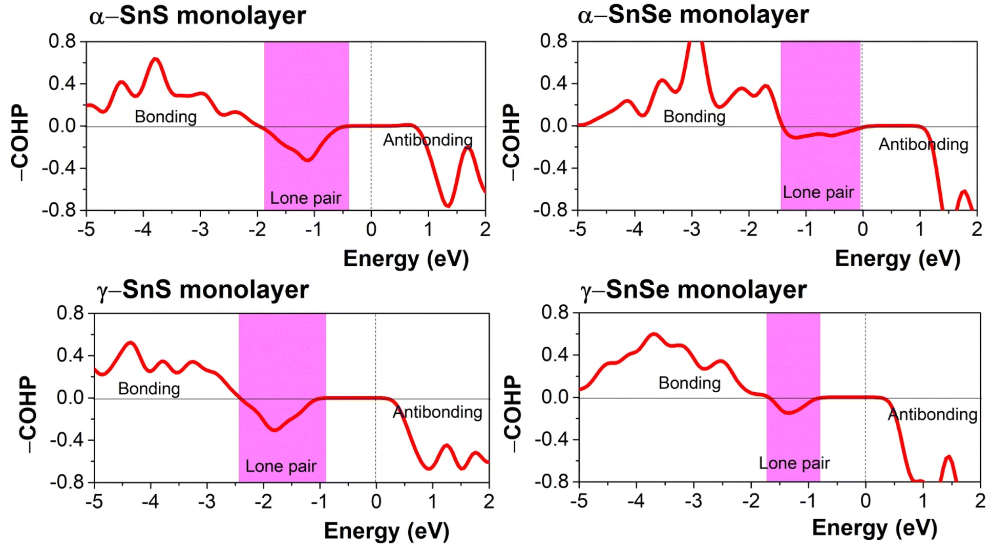 | ||
| Fig. 7 Calculated COHP of 2D monolayers of SnS and SnSe. The energy range of the lone pair is marked by the pink region in COHP, while the antibonding and bonding are displayed by negative and positive of –COHP. | ||
To quantify the difference between the lone pairs of 2D monolayers of SnS and SnSe, we calculated the integrated density of states (IDOS) for the antibonding region of lone pairs, determined by COHP calculation in Fig. 7. These results are represented in Table 3 for a quantitative comparison of the corresponding contributions of each component from Sn and chalcogen states to various hybridizations. The IDOS for lone pairs of γ-monolayers in Table 3 is larger than α-monolayers for all s and p states, confirming that the lone pairs of γ-monolayers are stronger than α-monolayers. IDOS of lone pairs in 2D SnSe is weaker than 2D SnS, which follows the general scheme of lone pairs in this group from ref. 12 and 13 due to the higher energy states of Se 4p than S 3p. We compared the contribution of each p-state in Sn and chalcogen for the 2D case with the reference value of bulk from Table 5 in the previous work.13 Interestingly, the contribution of one component in Sn 5p for 2D structures is dominant, while the other two are insignificant. Meanwhile, the contribution from Sn 5p is much weaker in the lone pairs of bulk. For 2D α-SnS and α-SnSe, the strongest contribution is found from the pz component while lesser IDOS were provided from the py and px components. Meanwhile, the lone pairs of 2D γ-SnS and γ-SnSe have remarkable contributions from px and pz components and one lesser contribution from the py component of S/Se. Bulk α and γ phases in the previous study of the lone pairs feature two motifs.13 The first motif of the α-bulk phase has two strong and one weak S/Se p-state contributions. Bulk γ-SnS and γ-SnSe correspond to the hybridization of one strong and two weak contributions from S/Se p-states. Hence, the lone pairs in our 2D structures do not follow the bulk, highlighting the sole contribution of one component of Sn 5p and the distinct contributions of S/Se p-states. Moreover, the stronger lone pairs of γ-monolayers could be the main reason for the remarkable expansion of the band gaps of monolayers compared to their bulks.
| Structure | Sn 5s | Sn total p-states | Sn 5px | Sn 5py | Sn 5pz | S/Se total p-states | S/Se px | S/Se py | S/Se pz |
|---|---|---|---|---|---|---|---|---|---|
| 2D α-SnS | 0.278 | 0.288 | 0.203 | 0.029 | 0.056 | 0.771 | 0.216 | 0.259 | 0.296 |
| 2D α-SnSe | 0.239 | 0.246 | 0.131 | 0.048 | 0.067 | 0.747 | 0.227 | 0.253 | 0.267 |
| 2D γ-SnS | 0.307 | 0.343 | 0.287 | 0.022 | 0.034 | 1.013 | 0.394 | 0.186 | 0.433 |
| 2D γ-SnSe | 0.248 | 0.325 | 0.248 | 0.023 | 0.054 | 0.948 | 0.393 | 0.187 | 0.368 |
3.2 Electronic transport properties of 2D monolayer for thermoelectric applications
Thermoelectric materials require a large Seebeck coefficient, high electrical conductivity, and low thermal conductivities. To assess the efficiency of function materials in thermoelectric devices these transport properties, and the power factor PF are considered to play an essential role.57 Therefore, we calculated them in both 2D and 3D SnS and SnSe to evaluate their efficiency in thermoelectric applications and results are presented in Fig. 8–10. We also compared these electronic transport properties in α and γ structures in 2D and bulk phases. | ||
| Fig. 8 (a) Calculated Seebeck coefficient S as a function of chemical potential μ (eV) at 300 K and 600 K for bulk 3D α and γ structures of SnS and SnSe. Seebeck coefficient S has negative values for n-type carrier μ > 0, while for p-type carrier in μ < 0, S has positive values. (b). Calculated Seebeck coefficient S as a function of chemical potential μ (eV) at 300 K and 600 K for 2D α and γ structures of SnS and SnSe. | ||
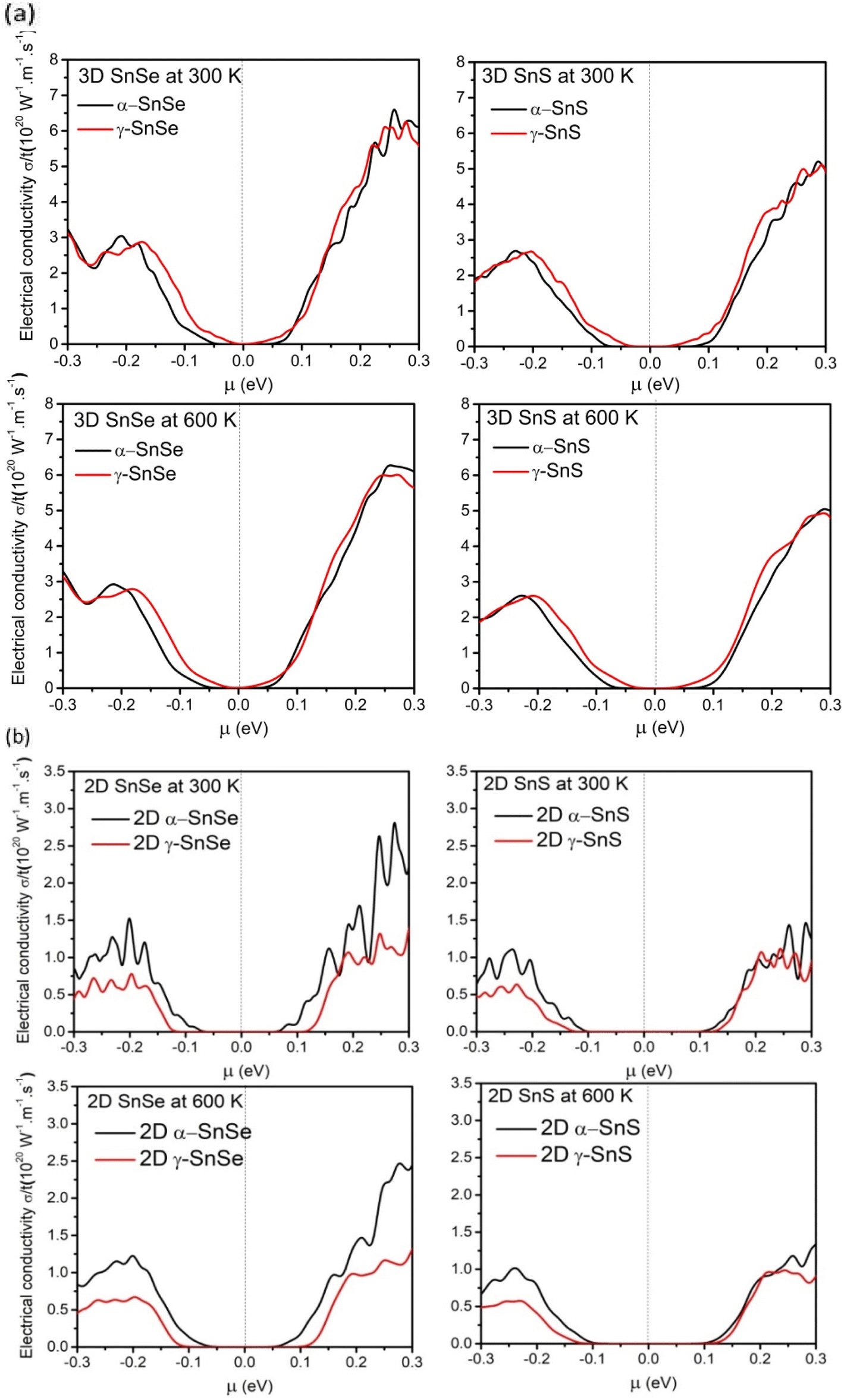 | ||
| Fig. 9 (a). Calculated relative electrical conductivity as a function of chemical potential μ (eV) at 300 K and 600 K for 3D α and γ structures of SnS and SnSe. (b). Calculated relative electrical conductivity σ/τ as a function of chemical potential μ (eV) at 300 K and 600 K for 2D α and γ structures of SnS and SnSe. | ||
 | ||
| Fig. 10 (a) Calculated relative power factor PF as a function of chemical potential μ (eV) at 300 K and 600 K for bulk 3D α and γ structures of SnS and SnSe. (b) Calculated relative power factor PF as a function of chemical potential μ (eV) at 300 K and 600 K for 2D α and γ structures of SnS and SnSe. | ||
The Seebeck coefficient of α and γ structures of SnS and SnSe were calculated at 300 K and 600 K in bulk phase (Fig. 8a) and 2D monolayer (Fig. 8b). For bulk α-SnS and α-SnSe, the peak value of Seebeck coefficients are estimated to be 1530 μV K−1 (α-SnSe) and 1032 μV K−1 (α-SnS) at 300 K and decrease upon heating to 600 K (540 μV K−1 for bulk α-SnSe and 850 μV K−1 for bulk α-SnS). This trend agrees with previous studies on bulk α-SnSe and α-SnS.46–48 Bulk γ-SnSe and γ-SnS show smaller Seebeck coefficients of 279 μV K−1 and 679 μV K−1 at 300 K that also drop to 186 μV K−1 and 355 μV K−1 at 600 K, respectively. This trend indicates that the maximum Seebeck coefficients decrease at high temperatures and bulk γ-SnSe/SnS possess overall lower Seebeck coefficients than their α-structure counterparts.48,65
For 2D structures in Fig. 8b, the conventional α-monolayers SnS and SnSe exhibit remarkably high peak values of Seebeck coefficients, around 1420–1480 μV K−1 at 300 K, and they decrease 730–1120 μV K−1 upon heating to 600 K, comparable to the other DFT reports.46,47 Hence, the Seebeck coefficient of 2D α-SnSe is higher than its bulk allotrope, while 2D-SnS has nearly the same value as bulk α-SnS. Upon increasing the temperature to 600 K, both Seebeck coefficients of 2D α-SnSe and α-SnS decrease, but to a value higher than in the bulk. Furthermore, peak values of Seebeck coefficients at 300 K for unconventional 2D γ monolayer SnS and SnSe are equal to α-structure, calculated around 1419–1460 μV K−1. Intriguingly, upon heating up to 600 K, the peaks of Seebeck coefficients for γ monolayers SnS and SnSe retain high values of 1370 μV K−1 for SnSe and 1440 μV K−1 for SnS. Thus, Seebeck coefficients of γ monolayers SnS and SnSe can maintain favorable values upon heating to high temperature, which is distinct compared to α-monolayers and bulk phases.
Further evaluating the thermoelectric ability of 2D monolayers of SnS and SnSe, we compared the relative electrical conductivity σ/τ (τ is the relaxation time) at 300 K and 600 K in Fig. 9. In Fig. 9a, we found only a slight difference in relative electrical conductivity between the bulk α and γ structures of SnS and SnSe. For 2D monolayers in Fig. 9b, our results are consistent with other studies as the monolayers have lower electrical conductivity due to their expanded band gap, and all structures exhibit the optimal electrical conductivity in n-type doping, which is generally preferred over the lower peak of electrical conductivity in p-type doping in SnS and SnSe.22,43,45,55 Comparing between 2D structures, we found that the electrical conductivity of α monolayers of SnS and SnSe are higher than γ monolayers. In addition, optimal peaks of electrical conductivity of 2D α and γ monolayers SnS are lower than SnSe. For both bulk and 2D monolayers, the overall electrical conductivity of SnS and SnSe decreases slightly upon increased temperature from 300 K to 600 K, consistent with previous findings.48,65
To further evaluate the transport properties of thermoelectric devices, we calculate the relative power factor, PF = σ2S/τ, and present results for bulk phases in Fig. 10a and for monolayers in Fig. 10b. Similar to previous studies on α-SnSe and α-SnS,46,48,65 the optimal power factor of bulk α-SnSe and α-SnS is enhanced upon increased temperature. High power factors of α-SnSe and α-SnS indicate their excellent performance in thermoelectric devices. Furthermore, comparing between bulk α and γ structures of SnS and SnSe, we found that the maximum power factors of γ structures of SnS and SnSe are comparable to their α-bulk allotropes, which could also be increased significantly if working in a high-temperature regime.
For 2D monolayers in Fig. 10b, at 300 K, the α-monolayer of SnSe exhibits the highest peak power factor at μ = 0.25, exceeding the maximum power factors of other monolayers of SnS and SnSe. Our result indicates that the optimal power factor of n-type doping is often preferred over p-type in α monolayers and γ monolayer SnSe, similar to the behavior of the bulk in Fig. 10a. An exception is the case of γ monolayers of SnS, which show a higher peak of power factor of p-type doping at 300 K. On the other hand, at 600 K, the maximum power factors of γ-monolayers increased considerably to higher values than that of α-monolayers. These results of optimal power factor suggest that γ monolayers of SnS and SnSe can achieve better values when increase to high temperature. Therefore, both 2D and 3D γ structures of SnS and SnSe have promising potential in thermoelectric applications, along with conventional α-structures.
4 Conclusions
In this study, we investigated the crystal structure, dynamical stability, electronic properties, and electronic transport characteristics of bulk and two-dimensional monolayer phases of SnS and SnSe, with a particular focus on the unconventional γ-phase. Our findings reveal that γ-SnS and γ-SnSe monolayers adopt distinct lattice configurations characterized by extended in-plane bonds and higher formation energies compared to their α-phase counterparts. Their surface energy, cleavage energy, and phonon dispersion confirm thermodynamic stability and suggest the feasibility of mechanical exfoliation from the bulk phase. Notably, the calculated cleavage energy for 2D γ-SnS and γ-SnSe at 0.69 J m−2 and 0.71 J m−2, respectively, predicts that mechanical exfoliation would be difficult and alternative methods such as liquid-phase exfoliation or chemical intercalation are suggested for synthesizing 2D γ-SnS and γ-SnSe.Electronic structure analysis indicates a significant band gap expansion in 2D γ-SnS and γ-SnSe, particularly in γ-SnSe monolayers. We found that 2D γ-monolayers express larger band gaps than 2D α-monolayers, while both bulk phases of γ-SnSe and γ-SnS possess narrower band gaps than their α-phase counterparts. This variation of the band-gap of 2D γ-SnSe and 2D α-SnSe could be the result of the effect of the lone pairs. Lone-pair interactions are found to be stronger in 2D γ-SnS and γ-SnSe than in their α-phase monolayer counterparts. Additionally, we identify a distinct enhancement of the Sn 5p state contribution and a modified role of the S/Se p-states in the lone-pair formation of the 2D γ-phase compared to the bulk. For the evaluation of electronic transport properties for thermoelectric applications, our theoretical approach provides a comparison of Seebeck coefficients, relative electrical conductivity and power factor as a function of the chemical potential, temperature, and relaxation time. These basic calculations are within the two approximations of the rigid band and constant electron relaxation time. Thus, our study encourages more research into this newly synthesized structure of SnSe and SnS in future work. Comparative assessment of the α- and γ-phases in both bulk and monolayer forms demonstrate that the Seebeck coefficients of γ-SnS and γ-SnSe remain robust at elevated temperatures. Furthermore, the thermoelectric power factors of both bulk and monolayer γ-phases are comparable to or exceed those of the conventional α-phase, underscoring their potential for high-efficiency thermoelectric applications. This work expands our understanding of SnS- and SnSe-based thermoelectric materials. It provides new insights into their structural distortion and electronic versatility, which is promised for next-generation energy conversion technologies.
Author contributions
Nguyen Truong Long: conceptualization, supervision, methodology, investigation, data curation, writing – original draft preparation, reviewing and editing. Huynh Anh Huy: conceptualization, investigation, writing, reviewing and editing. Neeraj Mishra: methodology, investigation, data curation, writing, reviewing and editing. Guy Makov: conceptualization, investigation, writing, reviewing and editing.Data availability
The data that support the findings of this study are available from the corresponding author upon reasonable request.Conflicts of interest
There are no conflicts to declare.Acknowledgements
This study is funded by the Can Tho University, Code: T2024-53.References
- S. Bai, X. Zhang and L. D. Zhao, Rethinking SnSe thermoelectrics from computational materials science, Acc. Chem. Res., 2023, 56(21), 3065–3075, DOI:10.1021/acs.accounts.3c00490
.
- M. R. Shankar and A. N. Prabhu, A review on structural characteristics and thermoelectric properties of mid-temperature range: chalcogenide-based thermoelectric materials, J. Mater. Sci., 2023, 58(43), 16591–16633, DOI:10.1007/s10853-023-09028-8
- J. Zheng, M. Ma, G. Yang, Y. Wu and D. Mei, Progress in the study of binary chalcogenide-based thermoelectric compounds, J. Solid State Chem., 2024, 334, 124617, DOI:10.1016/j.jssc.2024.124617
- X. Shi and Z. Ren, When IV–VI Meets I–V–VI2: A Reinvigorating Thermoelectric Strategy for Tin Monochalcogenides, Chem. Nano. Mat., 2023, 9(1), e202200396, DOI:10.1002/cnma.202200396
- L. D. Zhao, G. Tan, S. Hao, J. He, Y. Pei, H. Chi, H. Wang, S. Gong, H. Xu, V. P. Dravid and C. Uher, Ultrahigh power factor and thermoelectric performance in hole-doped single-crystal SnSe, Science, 2016, 351(6269), 141–144, DOI:10.1126/science.aad3749
- C. H. Ho, W. Y. Lin, L. C. Chao, K. Y. Lee, J. Inagaki and H. C. Hsueh, Study of structural, thermoelectric, and photoelectric properties of layered tin monochalcogenides SnX (X = S, Se) for energy application, ACS Appl. Mater. Interfaces, 2020, 3(5), 4896–4905, DOI:10.1021/acsaem.0c00481
- W. Shi, M. Gao, J. Wei, J. Gao and C. Fan, Tin Selenide (SnSe): Growth, Properties, and Applications, Adv. Sci., 2018, 5(4), 1700602, DOI:10.1002/advs.201700602
- M. Kumar, S. Rani, Y. Singh, K. S. Gour and V. N. Singh, Tin-selenide as a futuristic material: properties and applications, RSC Adv., 2021, 11, 6477–6503, 10.1039/d0ra09807h
- Y. Gong, Y. Li, Y. Li, M. Liu, Y. Bai and C. Wu, Metal Selenides Anode Materials for Sodium Ion Batteries: Synthesis, Modification, and Application, Small, 2023, 19(4), 2206194, DOI:10.1002/smll.202206194
- Y. Shen, Y. Zhang, J. Huo, X. Li, Z. Yan, Y. Pan, W. Sun, N. Deng and W. Kang, Two-dimensional SnSe material for solar cells and rechargeable batteries, J. Energy Storage, 2023, 69, 107958, DOI:10.1016/j.est.2023.107958
- C. Zhou, Y. K. Lee, Y. Yu, S. Byun, Z. Z. Luo, H. Lee, B. Ge, Y. L. Lee, X. Chen, J. Y. Lee and O. Cojocaru-Mirédin, Polycrystalline SnSe with a thermoelectric figure of merit greater than the single crystal, Nat. Mater., 2021, 20(10), 137, DOI:10.1038/s41563-021-01064-6
- D. J. Payne, R. G. Egdell, G. W. Watson and A. Walsh, Stereochemistry of post-transition metal oxides: revision of the classical lone pair model, Chem. Soc. Rev., 2011, 40, 4455–4463, 10.1039/C1CS15098G
- L. T. Nguyen and G. Makov, Lone-Pair Origins of Polymorphism: Sn Monochalcogenides as a Case Study, Chem. Mat., 2024, 36(11), 5487–5499, DOI:10.1021/acs.chemmater.4c00409
- L. D. Zhao, S. H. Lo, Y. Zhang, H. Sun, G. Tan, C. Uher and M. G. Kanatzidis, Ultralow thermal conductivity and high thermoelectric figure of merit in SnSe crystals, Nature, 2014, 508(7496), 373–377, DOI:10.1038/nature13184
- H. Lin, G. Tan, J. N. Shen, S. Hao, L. M. Wu, N. Calta, C. Malliakas, S. Wang, C. Uher, C. Wolverton and M. G. Kanatzidis, Concerted rattling in CsAg5Te3 leading to ultralow thermal conductivity and high thermoelectric performance, Angew. Chem., Int. Ed., 2016, 12(38), 11431–11436, DOI:10.1002/anie.201605015
- P.-F. Liu, X. Li, J. Li, J. Zhu, Z. Tong, M. Kofu, M. Nirei, J. Xu, W. Yin, F. Wang, T. Liang, Y. Zhang, D. J. Singh, J. Ma, H. Lin, J. Zhang, J. He and B.-T. Wang, Strong low-energy rattling modes enabled liquid-like ultralow thermal conductivity in a well-ordered solid, Natl. Sci. Rev., 2024, 11(12), nwae216, DOI:10.1093/nsr/nwae216
- M. González-Barrios, M. Tabuyo-Martínez, D. Ávila-Brande and J. Prado-Gonjal, Perspective on Crystal Structures, Synthetic Methods, and New Directions in Thermoelectric Materials, Small Struct., 2024, 2400136, DOI:10.1002/sstr.202400136
- B. Koren, R. E. Abutbul, V. Ezersky, N. Maman and Y. Golan, A new binary phase in the tin-monoselenide system: chemical epitaxy of orthorhombic γ-SnSe thin films, Mater. Chem. Front., 2021, 5(13), 5004–5011, 10.1039/D1QM00410G
- N. Zakay, A. Schlesinger, U. Argaman, L. Nguyen, N. Maman, B. Koren, M. Ozeri, G. Makov, Y. Golan and D. Azulay, Electrical and Optical Properties of γ-SnSe: A New Ultra-narrow Band Gap Material, ACS Appl. Mater. Interfaces, 2023, 15(12), 15668–15675, DOI:10.1021/acsami.2c22134
- R. E. Abutbul, E. Segev, U. Argaman, G. Makov and Y. Golan, π-Phase Tin and Germanium Monochalcogenide Semiconductors: An Emerging Materials System, Adv. Mater., 2018, 30, 1–8, DOI:10.1002/adma.201706285
- R. E. Abutbul, E. Segev, L. Zeiri, V. Ezersky, G. Makov and Y. Golan, Synthesis and properties of nanocrystalline π-SnS–a new cubic phase of tin sulphide, RSC Adv., 2016, 6(7), 5848–5855, 10.1039/C5RA23092F
- A. S. Sarkar, I. Konidakis, E. Gagaoudakis, G. M. Maragkakis, S. Psilodimitrakopoulos, D. Katerinopoulou, L. Sygellou, G. Deligeorgis, V. Binas, I. M. Oikonomou and P. Komninou, Liquid phase isolation of SnS monolayers with enhanced optoelectronic properties, Adv. Sci., 2023, 10(6), 2201842, DOI:10.1002/advs.202201842
- H. Khan, N. Mahmood, A. Zavabeti, A. Elbourne, M. A. Rahman, B. Y. Zhang, V. Krishnamurth, P. Atkin, M. B. Ghasemian, J. Yang and G. Zheng, Liquid metal-based synthesis of high performance monolayer SnS piezoelectric nanogenerators, Nat. Comm., 2020, 11(1), 3449, DOI:10.1038/s41467-020-17296-0
- L. Li, Z. Chen, Y. Hu, X. Wang, T. Zhang, W. Chen and Q. Wang, Single-layer single-crystalline SnSe nanosheets, J. Am. Chem. Soc., 2013, 135(4), 1213–1216 Search PubMed
- S. Tamuli, A. Kar and D. Mohanta, Liquid phase exfoliation of α-SnSe nanosheets: exploring the role of solvents, J. Phys. Conf. Ser., 2024, 2919(1), 012006, DOI:10.1088/1742-6596/2919/1/012006
- A. K. Singh and R. G. Hennig, Computational prediction of two-dimensional group-IV mono-chalcogenides, Appl. Phys. Lett., 2014, 105, 042103, DOI:10.1063/1.4891230
- M. Zhou, X. Chen, M. Li and A. Du, Widely tunable and anisotropic charge carrier mobility in monolayer tin (II) selenide using biaxial strain: a first-principles study, J. Mater. Chem. C, 2017, 5(5), 1247–1254, 10.1039/C6TC04692D
- J.
W. Villanova and S. Barraza-Lopez, Anomalous thermoelectricity at the two-dimensional structural transition of SnSe monolayers, Phys. Rev. B, 2021, 103(3), 035421, DOI:10.1103/PhysRevB.103.035421
- R. Gupta, S. Kakkar, B. Dongre, J. Carrete and C. Bera, Enhancement in the thermoelectric performance of SnS monolayer by strain engineering, ACS Appl. Mater. Interfaces, 2023, 6(7), 3944–3952, DOI:10.1021/acsaem.3c00110
- S.-D. Guo and Y.-H. Wang, Thermoelectric properties of orthorhombic group IV–VI monolayers from the first-principles calculations, J. Appl. Phys., 2017, 121, 034302, DOI:10.1063/1.4974200
- B. Dong, Z. Wang, N. T. Hung, A. R. Oganov, T. Yang, R. Saito and Z. Zhang, New two-dimensional phase of tin chalcogenides: candidates for high-performance thermoelectric materials, Phys. Rev. Mater., 2019, 3(1), 013405, DOI:10.1103/PhysRevMaterials.3.013405
- Y. Hu, K. Y. Li, Y. Lu, Y. Huang and X. H. Shao, High thermoelectric performances of monolayer SnSe allotropes, Nanoscale, 2017, 9(41), 16093–16100, 10.1039/C7NR04766E
- C. Zhu, T. Feng, X. Jiang, G. Li, J. H. Yuan, C. Liu, P. Zhang and J. Wang, Electronic, mechanical and gas sensing properties of two-dimensional γ-SnSe, Phys. Chem. Chem. Phys., 2023, 25(42), 28716–28726, 10.1039/D3CP03483F
- S. S. Nair, M. Sajjad, K. Biswas and N. Singh, Metavalent Bonding Induced Phonon Transport Anomaly in 2D γ-MX (M = Ge, Sn, Pb Nair and Se, Te) Monolayers, ACS Appl. Mater. Interfaces, 2023, 6(17), 8787–8793, DOI:10.1021/acsaem.3c01118
- P. Giannozzi, O. Andreussi, T. Brumme, O. Bunau, M. B. Nardelli, M. Calandra, R. Car, C. Cavazzoni, D. Ceresoli, M. Cococcioni, N. Colonna, I. Carnimeo, A. D. Corso, S. de Gironcoli, P. Delugas, R. A. DiStasio Jr, A. Ferretti, A. Floris, G. Fratesi, G. Fugallo, R. Gebauer, U. Gerstmann, F. Giustino, T. Gorni, J. Jia, M. Kawamura, H.-Y. Ko, A. Kokalj, E. Küçükbenli, M. Lazzeri, M. Marsili, N. Marzari, F. Mauri, N. L. Nguyen, H.-V. Nguyen, A. Otero-de-la-Roza, L. Paulatto, S. Poncé, D. Rocca, R. Sabatini, B. Santra, M. Schlipf, A. P. Seitsonen, A. Smogunov, I. Timrov, T. Thonhauser, P. Umari, N. Vast, X. Wu and S. Baroni, Advanced capabilities for materials modelling with Quantum ESPRESSO, Phys. Rev. B:Condens. Matter Mater. Phys., 2017, 29(46), 465901, DOI:10.1088/1361-648X/aa8f79
- K. F. Garrity, J. W. Bennett, K. M. Rabe and D. Vanderbilt, Pseudopotentials for high-throughput DFT calculations, Comput. Mater. Sci., 2014, 81, 446–452, DOI:10.1016/j.commatsci.2013.08.053
- A. Dal Corso, Pseudopotentials periodic table: From H to Pu, Comput. Mater. Sci., 2014, 95, 337–350, DOI:10.1016/j.commatsci.2014.07.043
- K. Burke, M. Ernzerhof and J. P. Perdew, Generalized Gradient Approximation Made Simple, Phys. Rev. Lett., 1996, 7, 3865, DOI:10.1103/PhysRevLett.77.3865
- J. P. Perdew, M. Ernzerhof and K. Burke, Rationale for mixing exact exchange with density functional approximations, J. Chem. Phys., 1996, 105, 9982–9985, DOI:10.1063/1.472933
- K. Lee, É. D. Murray, L. Kong, B. I. Lundqvist and D. C. Langreth, Higher-accuracy van der Waals density functional, Phys. Rev. B:Condens. Matter Mater. Phys., 2010, 82(8), 081101, DOI:10.1103/PhysRevB.82.081101
- D. Chakraborty, K. Berland and T. Thonhauser, Next-generation nonlocal van der Waals density functional, J. Chem. Theory Comput., 2020, 16(9), 5893–5911, DOI:10.1021/acs.jctc.0c00471
- H. J. Monkhorst and J. D. Pack, Special points for Brillouin-zone integrations, Phys. Rev., 1976, 13(12), 5188–5192, DOI:10.1103/PhysRevB.13.5188
- S. de Gironcoli, A. D. Corso and P. G. S. Baroni, Phonons and related crystal properties from density-functional perturbation theory, Rev. Mod. Phys., 2001, 73, 515, DOI:10.1103/RevModPhys.73.515
- R. Nelson, C. Ertural, J. George, V. L. Deringer, G. Hautier and R. Dronskowski, LOBSTER: local orbital projections, atomic charges, and chemical-bonding analysis from projector-augmented-wave-based density-functional theory, J. Comput. Chem., 2020, 41(21), 1931–1940, DOI:10.1002/jcc.26353
- G. K. H. Madsen, J. Carrete and M. J. Verstraete, BoltzTraP2, a program for interpolating band structures and calculating semi-classical transport coefficients, Comput. Phys. Commun., 2018, 231, 140–145, DOI:10.1016/j.cpc.2018.05.010
- G. Ding, Y. Hu, D. Li and X. Wang, A comparative study of thermoelectric properties between bulk and monolayer SnSe, Results Phys., 2019, 15, 102631, DOI:10.1016/j.rinp.2019.102631
- A. Shafique and Y. H. Shin, Thermoelectric and phonon transport properties of two-dimensional IV–VI compounds, Sci. Rep., 2017, 7(1), 506, DOI:10.1038/s41598-017-00598-7
- G. Ding, G. Gao and K. Yao, High-efficient thermoelectric materials: The case of orthorhombic IV-VI compounds, Sci. Rep., 2015, 5(1), 9567, DOI:10.1038/srep09567
- F. O. von Rohr, H. Ji, F. A. Cevallos, T. Gao and N. P. Ong, High-Pressure Synthesis and Characterization of β-GeSe, A SixMembered-Ring Semiconductor in an Uncommon Boat, J. Am. Chem. Soc., 2017, 139, 2771–2777, DOI:10.1021/jacs.6b12828
- J. T. Paul, A. K. Singh, Z. Dong, H. Zhuang, B. C. Revard, B. Rijal, M. Ashton, A. Linscheid, M. Blonsky, D. Gluhovic and J. Guo, Computational methods for 2D materials: discovery, property characterization, and application design, J. Phys.:Condens. Matter, 2020, 32(15), 159501, DOI:10.1088/1361-648X/ab5768
- K. Momeni, Y. Ji, Y. Wang, S. Paul, S. Neshani, D. E. Yilmaz, Y. K. Shin, D. Zhang, J. W. Jiang, H. S. Park, S. Sinnott, A. v. Duin, V. Crespi and L.-Q. Chen, Multiscale computational understanding and growth of 2D materials: a review, Comput. Mater. Sci., 2020, 6(1), 22, DOI:10.1038/s41524-020-0280-2
- Y. Xu, K. Xu, C. Ma, Y. Chen, H. Zhang, Y. Liu and Y. Ji, Novel two-dimensional β-GeSe and β-SnSe semiconductors: anisotropic high carrier mobility and excellent photocatalytic water splitting, J. Mater. Chem. A, 2020, 8(37), 1961, 10.1039/D0TA06299E
- F. Li, X. Liu, Y. Wang and Y. Li, Germanium monosulfide monolayer: a novel two-dimensional semiconductor with a high carrier mobility, J. Mater. Chem. C, 2016, 4(11), 2155–2159, 10.1039/C6TC00454G
- U. Argaman, R. E. Abutbul, Y. Golan and G. Makov, Phonon band gaps in the IV-VI monochalcogenides, Phys. Rev. B, 2019, 100(5), 054104, DOI:10.1103/PhysRevB.100.054104
- M. Hong, Y. Wang, T. Feng, Q. Sun, S. Xu, S. Matsumura, S. T. Pantelides, J. Zou and Z. G. Chen, Strong phonon–phonon interactions securing extraordinary thermoelectric Ge1–xSbxTe with Zn-alloying-induced band alignment, J. Am. Chem. Soc., 2018, 141(4), 1742–1748, DOI:10.1021/jacs.8b12624
- J. S. Kang, M. Li, H. Wu, H. Nguyen and Y. Hu, Experimental observation of high thermal conductivity in boron arsenide, Science, 2018, 361(6402), 575–578, DOI:10.1126/science.aat5522
- Y. Zhang, B. Shang, L. Li and J. Lei, Coupling effects of strain on structural transformation and bandgap engineering in SnS monolayer, RSC Adv., 2017, 7(48), 30327–30333, 10.1039/C7RA04507G
- A. Batool, Y. Zhu, X. Ma, M. I. Saleem and C. Cao, DFT study of the structural, electronic, and optical properties of bulk, monolayer, and bilayer Sn-monochalcogenides, Appl. Surf. Sci. Adv., 2022, 11, 100275, DOI:10.1016/j.apsadv.2022.100275
- Y. Sun, Z. Shuai and D. Wang, Reducing lattice thermal conductivity of the thermoelectric SnSe monolayer: role of phonon–electron coupling, J. Phys. Chem. C, 2019, 123(18), 12001–12006, DOI:10.1021/acs.jpcc.9b02344
- P. D. Antunez, J. J. Buckley and R. L. Brutchey, Tin and germanium monochalcogenide IV–VI semiconductor nanocrystals for use in solar cells, Nanoscale, 2011, 3(6), 2399–2411, 10.1039/C1NR10084J
- Y. Li, M. Wu, D. K. Song, T. Ding, F. Liu, J. Li, H. Zhang and H. Xie, Transport and thermoelectric properties of SnX (X = S or Se) bilayers and heterostructures, ACS Appl. Mater. Interfaces, 2020, 3(7), 6946–6955, DOI:10.1021/acsaem.0c01020
- A. K. Deb and V. Kumar, Bandgap engineering in semiconducting one to few layers of SnS and SnSe, Phys. Status Solidi B, 2017, 254(2), 1600379, DOI:10.1002/pssb.201600379
- X. Wang, Z. Liu, X. G. Zhao, J. Lv, K. Biswas and L. Zhang, Computational design of mixed-valence tin sulfides as solar absorbers, ACS Appl. Mater. Interfaces, 2019, 11(28), 24867–24875, DOI:10.1021/acsami.9b01223
- A. Walsh and G. W. Watson, Influence of the anion on lone pair formation in Sn (II) monochalcogenides: a DFT study, J. Phys. Chem. B, 2005, 109(40), 18868–18875, DOI:10.1021/jp051822r
- F. Q. Wang, S. Zhang, J. Yu and Q. Wang, Thermoelectric properties of single-layered SnSe sheet, Nanoscale, 2015, 7(38), 15962–15970, 10.1039/C5NR03813H
Footnote |
| † Electronic supplementary information (ESI) available: Structural data for 2D and bulk SnS and SnSe phases. See DOI: https://doi.org/10.1039/d5ra01965f. |
| This journal is © The Royal Society of Chemistry 2025 |