
 Open Access Article
 This Open Access Article is licensed under a
 Creative Commons Attribution 3.0 Unported Licence
A high-performance “fueled” photodetector based on few-layered 2D ternary chalcogenide NiGa2S4†
Marco
Serra
*afg,
Nikolas
Antonatos
 a,
Jan
Luxa
a,
Luc
Lajaunie
bc,
Josep
Albero
d,
Agata
Sabik
e,
Wojciech M.
Linhart
e,
Hermenegildo
Garcia
d,
Robert
Kudrawiec
e,
David
Sedmidubský
a and
Zdenek
Sofer
*a
a,
Jan
Luxa
a,
Luc
Lajaunie
bc,
Josep
Albero
d,
Agata
Sabik
e,
Wojciech M.
Linhart
e,
Hermenegildo
Garcia
d,
Robert
Kudrawiec
e,
David
Sedmidubský
a and
Zdenek
Sofer
*a
aDepartment of Inorganic Chemistry, University of Chemistry and Technology, Prague, Technická 5, 16228, Prague, Czech Republic. E-mail: soferz@vscht.cz; serram@vscht.cz
bDepartamento de Ciencia de los Materiales e Ingenieria Metalúrgica y Química Inorgánica, Facultad de ciencia, Universidad de Cádiz, Campus Río San Pedro S/N, Puerto Real, 11510, Cádiz, Spain
cInstituto Universitario de Investigación de Microscopía Electrónica y Materiales (IMEYMAT), Facultad de Ciencias, Universidad de Cádiz, Campus Río San Pedro S/N, Puerto Real 11510, Cádiz, Spain
dInstituto de Tecnología Química, Universitat Politécnica de Valencia – Consejo Superior de Investigación Científicas (UPV-CSIC), Universitat Politècnica de Vàlencia, Avda. de los Naranjos S/N, 46022, Valencia, Spain
eDepartment of Semiconductor Materials Engineering, Wroclaw University of Scienceand Technology, Wybreże Wyspiańskiego 27, 50-270, Wrocław, Poland
fCentro H2–MORE, Università di Modena e Reggio Emilia, 41125 Modena, Italy
gDipartimento di Scienze Chimiche e Geologiche, Università di Modena e Reggio Emilia, Via G. Campi 103, 41125 Modena, Italy
First published on 10th April 2023
Abstract
Few-layered binary 2D transition metal chalcogenides have been comprehensively employed in photodetector systems thanks to their intrinsic band gap structure and a high in-plane charge carrier mobility. Their rich chemistry is further broadened when considering ternary 2D chalcogenide materials, giving the possibility to prepare isomorphic materials characterized by various metal distributions within the framework of a crystal structure. Whereas the “inverse” A(τ)B(Ω)(τ)2X4 hexagonal structures (e.g. ZnIn2S4) have been widely studied in photocatalysis, “normal” AII(Ω) BIII(τ)2XVI4 phases have not been considered so far. In this study, a NiGa2S4 photodetector has been prepared by drop-casting the exfoliated crystals onto ITO glass. Their photoresponse has been analyzed either in the absence or in the presence of an electron donor species (EtOH) in the electrolyte solution. Ethanol acts as a fuel in the PEC photodetector system boosting their performance by a factor of ∼x49 in terms of the responsivity at a given wavelength. Moreover, the spectral response is expanded from blue to far IR wavelengths, reaching responsivity values from 48 to 7 mA W−1. The dynamics of photogenerated electrons and holes has been studied using laser flash photolysis. The stability of the “fueled” PEC photodetector has been evaluated through long-term tests which have shown a stable response over extended periods. It is anticipated that the present work can provide fundamental insight into the field of PEC semiconductor-based photodetectors, offering an extendable strategy to engineer high-performance PEC devices.
1. Introduction
2D chalcogenide materials have attracted the interest of many researchers as potential candidates for next-generation (opto)electronic,1 spintronic,2 and catalytic devices3 due to their distinctive structure which combines features such as large, exposed surfaces, anisotropic bonding patterns, and short charge carrier diffusion length. Layered transition metal chalcogenides (TMC, e.g., MoS2 and WS2) have opened up new avenues for a wide class of novel electronic nanodevices owing to their typical van der Waals structure,4 which allow the achievement of layered crystals with reduced dimensionality. Nanostructured optoelectronic devices, such as photodetectors, transistors, and pseudocapacitors based on few-layered TMC materials have been studied thoroughly.5Binary monochalcogenide, dichalcogenide, and trichalcogenide (e.g., GaSe,6 WS2,7 and In2S38) photo-responsive devices have been studied in great detail, in contrast, ternary 2D chalcogenides materials are lagging behind. Typically, ternary chalcogenide materials are characterized by the presence of multiple degrees of freedom which introduces the possibility of obtaining various phases.9 A plenitude of structures can be identified using the general formula AxByXz, ranging from 1D-, 2D- to 3D-structures.10 In the case of AIIBIII2XVI4 compounds, layered hexagonal ZnIn2S4-type structures are obtained when octahedral (Ω) and tetrahedral (τ) sites are present in the relationship 1(Ω): 2(τ). This structure is described by the intercalation of an octahedral sheet into a double layer of tetrahedral sheets as described using the formula S–M(τ)–S–M(Ω)–S–M(τ)–S.11 The position of the cationic species within octahedral and tetrahedral sites can assume two configurations, denominated as “normal” (A(Ω)B(τ)2X4; e.g. MgAl2Se412) and “inverse” (A(τ)B(Ω), B(τ)X4e.g. ZnIn2S4).13 Extended efforts have been devoted to the synthesis, design, and study of various photocatalytic systems, based on the “inverse” hexagonal ZnIn2S4 in various applications14 and we have recently shown that ZnIn2S4 crystals can be used to produce a high-performance visible light-NIR photodetector based on crystalline flakes, which can be readily integrated into wearable devices.15
In contrast, “normal” AIIBIII2XVI4 structures have been investigated more rarely.16 NiGa2S4 is a typical ordered triangular system, in which antiferromagnetic properties have been described in great detail in the literature.17 NiGa2S4 has been employed in a solid-state supercapacitor in combination with graphene oxide as well.18 On the other hand, its photoelectronic properties have been completely overlooked. Herein, we describe a novel “fueled” photodetector system based on few-layered NiGa2S4 crystals deposited on ITO glass. In photodetector systems, a specific set of lights is used as an input to induce a photocurrent, which is readily measured providing the output of the device. An ideal photodetector should present characteristics like high responsivity and quick and defined response to a specific set of wavelengths accordingly to the intensity of the irradiation.19 Typically, their response is studied under different conditions, such as alkaline or acid media, optimizing their performances as a function of material loading or the processing of the photoresponsive material. Conceivably, the photoresponse of a semiconductor-based photodetector is in close resemblance with the absorbance of the material, however, the detection of a low-power signal in the NIR-IR zone is frequently challenging due to the fast recombination of photogenerated charge carriers.20 In supported photodetector systems this effect is mitigated by the application of an external bias on the working electrode directing the charge migration thereby with the effect of inhibiting the charge recombination phenomena.21 In the case of an unsupported semiconductor-based photocatalytic system (i.e., H2 and O2 production and CO2 reduction in suspension) a different strategy is applied; the charge recombination is inhibited by the presence of electrons or hole scavengers in solution, such as EtOH and AgNO3.22
In some cases, the presence of electron donors causes an increment of the photocatalytic activity, in other cases it allows the attainment of a photoproduct otherwise hindered, acting as a fuel for the propelling of the reaction.23 In the present study, a combination of both strategies is used to explore the photocatalytic activity of NiGa2S4-based photodetectors. First, the photocatalytic activity of exfoliated NiGa2S4 nanocrystals supported on ITO under an external bias is presented. In the absence of electron donors, the photodetector shows a selective response limited to purple light (λ = 420 nm) with values of responsivity in the order of 1 mA W−1. When an external bias is applied in the presence of an electron donor (EtOH) mixed in an electrolyte solution the photoresponse undergoes a substantial modification in terms of responsivity and spectral response. “Fueled” NiGa2S4 photodetectors are characterized by an increment of ∼49× in terms of responsivity for purple light. Furthermore, the photoresponse of the system is expanded in all the visible range up to the far IR zone (λ = 940 nm) with values of responsivity in the order of 7 mA W−1. To the best of our knowledge, the use of an electron donor in photosensitive devices has not been explored so far. The use of this resource shows unforeseen properties for such a “fueled” photodetector allowing the attainment of a specific spectral response with incremented detectivity as a function of a chemical stimulus such as the presence of an electron donor in the electrolyte solution. This work could facilitate follow-up experiments in the photodetector field introducing a new element to improve and fine-tune the properties of well-known systems to upgrade their performances.
2. Results and discussion
NiGa2S4 crystals (inset Fig. 1b) were prepared using a Chemical Vapour Transport (CVT) technique starting from a stoichiometric mixture of the elements in the presence of a small amount of I2 acting as the transport agent.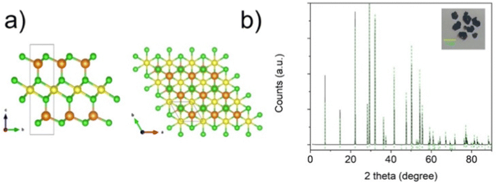 | ||
| Fig. 1 Crystalline structure of hexagonal NiGa2S4 along the c-axis and the ab plane. (b) XRD pattern of NiGa2S4 crystalline powder. In the inset a sample of the crystals obtained via CVT synthesis is shown. The indexed XRD pattern of the NiGa2S4 crystals and powders are shown in Fig. S1 and S2 (ESI†), respectively. | ||
The as prepared materials were characterized by X-ray diffraction, SEM and HRTEM, Raman, and UV-Vis spectroscopy. The X-ray diffraction pattern is depicted in Fig. 1 showing the characteristic peaks of the hexagonal P![[3 with combining macron]](https://www.rsc.org/images/entities/char_0033_0304.gif) m1 phase (Reference code: 04-005-3896) with lattice parameters of a, b = 3.63 Å and c = 12.01 Å.24 The crystal structure is represented in Fig. 1a. The unit cell contains a single crystalline 7-atom slab with a thickness of 9 Å. The NiS6 octahedra form a triangular layer in the ab plane interposed between two tetrahedral GaS4 layers along the c axis.
m1 phase (Reference code: 04-005-3896) with lattice parameters of a, b = 3.63 Å and c = 12.01 Å.24 The crystal structure is represented in Fig. 1a. The unit cell contains a single crystalline 7-atom slab with a thickness of 9 Å. The NiS6 octahedra form a triangular layer in the ab plane interposed between two tetrahedral GaS4 layers along the c axis.
The electronic structure around the Fermi level (Fig. 2) calculated with the MedeA-VASP using the hybrid functional (HSE6) shows the characteristic features of the involved element valence states in the respective crystal field environment. The valence bands of predominantly S-3p character are intermixed with spin polarized Ni-3d states split in the trigonally distorted octahedral field (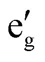 + a1g+ eg) carrying the net spin moment 1.55/Ni. The conduction band separated by a band gap of 1.95 eV is mainly contributed by spin-down Ni-eg and Ga-4s.
 | ||
| Fig. 2 Calculated electronic structure of NiGa2S4. (a) Band structure along principal directions of the first Brillouin zone. (b) Density of states (DOS) for the spin-up (↑) and spin-down (↓) channels including PDOS for Ni-3d states. | ||
Although the band structure plotted in Fig. 2a apparently shows a direct gap at the Γ-point of the first Brillouin zone, the valence band maximum is in fact slightly shifted towards (0.11, −0.11, 0.33) while the conduction band minimum is really located at the Γ-point.
The Raman spectra (Fig. S3, ESI†) present the distinctive feature of NiGa2S4 previously reported by M. E. Valentine et al.25 characterized by two intense A1g peaks at 122 and 454 cm−1, and two Eg and A1g vibration modes at 211 and 317 cm−1 of minor intensity.
The crystals were further characterized by SEM-EDS analysis. As shown in Fig. S4 (ESI†), the crystals submitted to mechanical exfoliation using the scotch tape method present the typical feature of layered materials. The SEM-EDS analysis provides an elemental identification analysis in agreement with the expected stoichiometry. SEM-EDS analysis of the powder obtained by grinding NiGa2S4 crystals after a period of 3 months being exposed to the air (Fig. S5, ESI†) shows no perceptible trace of oxidation, highlighting the stability of the material in the air over extended periods.
Fig. 3 shows the (S)TEM analysis performed on the NiGa2S4 flake. The size of the flakes is typically between 1 and 2 μm. The elemental quantification was extracted from the EDS spectrum (Fig. 3a and b) and is shown in Fig. S4 in the ESI.† The composition is close to the expected stoichiometry. According to the EDS maps (Fig. S6, ESI†), the flake appears homogeneous in composition. Fig. 3c shows the SAED pattern acquired on the same flake. It was successfully indexed as corresponding to the NiGa2S4 crystal structure seen along the [0 0 1] zone axis.26
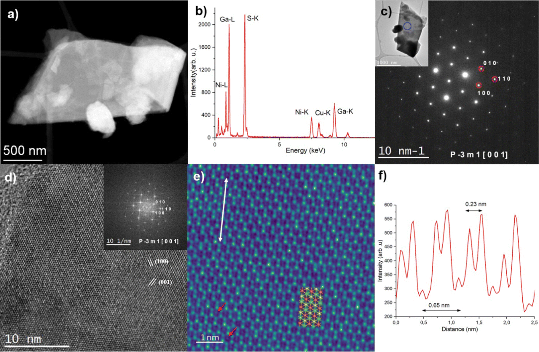 | ||
| Fig. 3 (a) Low magnification STEM-HAADF image of a NiGa2S4 flake. (b) Corresponding EDS spectrum. (c) SAED pattern acquired on the same flake successfully indexed as corresponding to the NiGa2S4P-3m1 crystal structure seen along the [0 0 1] (=[0 0 0 1]) zone axis. The inset displays the corresponding low-magnification TEM image, and the blue circle highlights the area used to acquire the SAED pattern. (d) HR-TEM image acquired on a thin area of the same flake. The inset shows the corresponding FFT pattern. It has been successfully indexed as belonging to the NiGa2S4Pm1 crystal structure seen along the [0 0 1] (=[0 0 0 1]) zone axis. (e) Filtered HR-TEM image corresponding to an enlarged view of Fig. 3d. It is superposed with the NiGa2S4 atomic structure as seen along the [0 0 1] zone axis (Ni: orange, Ga: green, S: yellow). The red arrows highlight the presence of Ni atoms, and the white arrow highlights the area used to extract the intensity profile shown in (b). (f) Intensity profile extracted from the HR-TEM image (white arrow, Fig. 3e). | ||
Fig. 3d shows the HR-TEM image acquired on a thin area of the same flake. The high crystalline quality of the flake can be highlighted from both the HR-TEM image and the corresponding FFT pattern. It should be noted that the FFT pattern was successfully automatically indexed with less than 1% error on both the distances and angles as corresponding to the NiGa2S4 crystal structure seen along the [0 0 1] (=[0 0 0 1]) zone axis. Fig. 3a shows the filtered HR-TEM image corresponding to an enlarged view of Fig. 3d. In particular, the Ni atoms which are situated in this projection at the center of the Ga/S hexagons can be clearly highlighted (red arrows in Fig. 3e). Fig. 3f shows the intensity profile extracted from the HR-TEM image (cf. white arrow in Fig. 3e). Along this direction, the Ni atoms are separated by 0.65 nm and the atoms of the Ga/S doublet are separated by 0.23 nm. These values are in excellent agreement with the expected one: 0.63 nm and 0.21 nm, respectively.
The samples were also characterized in terms of their surface composition by X-ray photoelectron spectroscopy (XPS) with high-resolution core-level spectra displayed in Fig. S7 (ESI†). Fig. S7a (ESI†) clearly illustrates only one oxidation state of Ni as supported by the distinguished peak located at ca. 855 eV, well in agreement with previous reports on this material.18 Similarly, the Ga 2p core-level spectrum (Fig. S7b, ESI†) displays two singular peaks located at previously reported positions,18 without any signs of surface oxidation, thus proving the high quality of our material. Finally, the S 2s core-level spectrum in Fig. 7c is shown instead of S 2p due to overlap with the Ga 3s peak. However, the spectrum clearly demonstrates one singlet corresponding to sulfidic ions without any trace of oxidation.
In Fig. 4 a representative AFM image of NiGa2S4 flakes with its corresponding height profile is depicted indicating that the resulting flakes from the ultrasonication process had a thickness of 12 nm with a 1 μm lateral size. According to the c = 12.01 Å lattice parameter of the material, the flakes correspond to 10 layers.26 In addition, we have provided in the ESI† the investigation of more NiGa2S4 flakes with various lateral sizes and thicknesses in order to provide full surveillance of the exfoliation procedure (Fig. S8, ESI†). The thickness of the flakes varied between 12–80 nm.
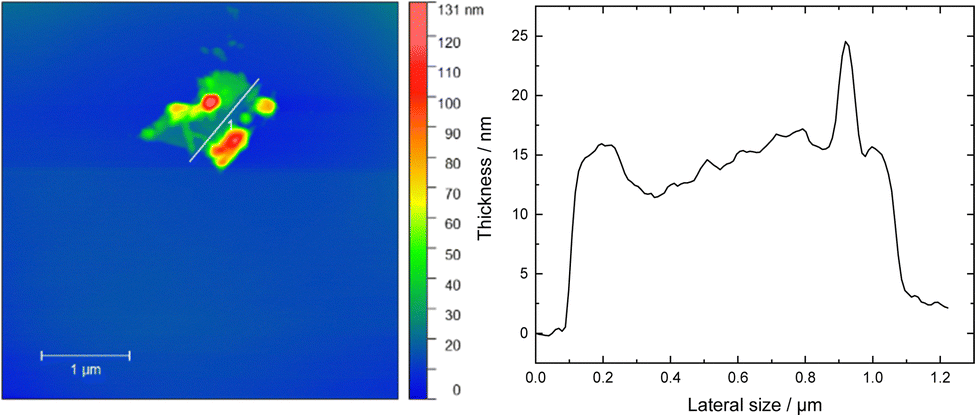 | ||
| Fig. 4 AFM image and the corresponding height profile plot of exfoliated NiGa2S4. | ||
In order to investigate the light-harvesting properties of the exfoliated crystalline sheets, the absorbance spectrum of a NiGa2S4 DMF suspension was recorded. As represented in Fig. 5, the absorbance profile is characterized by a broadband spanning the visible and infrared wavelength region, which highlights the possibility of having a photoelectrochemical response within a wide range of frequencies. The curve obtained using the Tauc plot method reveals a band gap value in the order of 1.78 eV in accord with the value reported in the literature for bulk NiGa2S4 crystals,27 and is slightly lower compared to the theoretical band gap predicted by hybrid functional ab initio calculations. The experimental value of the band gap for bulk NiGa2S4 has not been published so far. Moreover, no optical studies for NiGa2S4 have been reported so far and therefore these studies have been carried out.
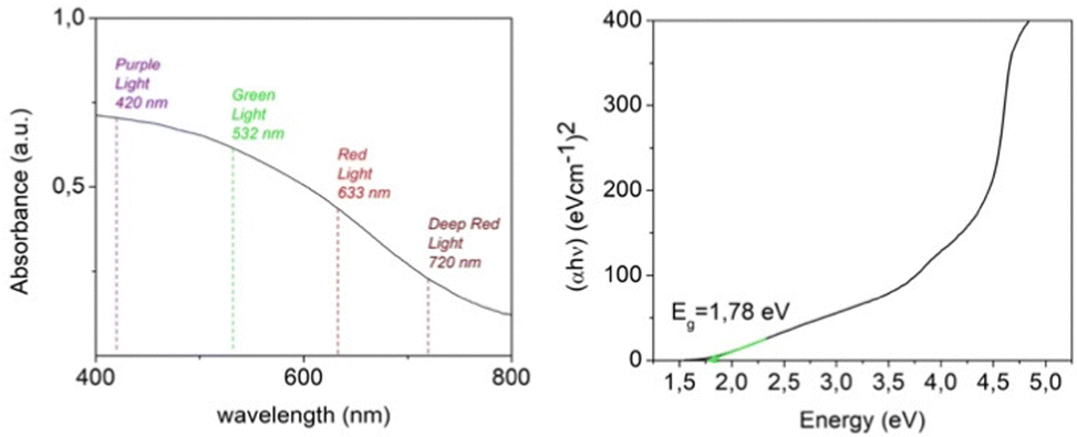 | ||
| Fig. 5 (a) UV-Vis absorbance spectrum of an exfoliated NiGa2S4 DMF suspension. The wavelength of the LED light source employed for the PEC study is marked by dashed lines. (b) Tauc plot used to extract the optical band gap of NiGa2S4 nanosheets. | ||
Fig. 7a shows the transmission and reflection spectra for bulk NiGa2S4 in the NIR-VIS range. These spectra clearly show that the semitransparency region covers the NIR and ends at ∼800 nm where we deal with interband absorption. On the basis of the transmission and reflection measurements, absorption spectra were obtained to determine the absorption edge. Fig. 7b shows the absorption spectra in the vicinity of the absorption edge obtained for different temperatures. A clear shift of the absorption edge towards higher energies is visible as the temperature decreases which is typical for III–V semiconductors28 and van der Waals semiconductors.
In order to determine the energy of the absorption edge and its nature, both the square root and square of the absorption spectrum, which corresponds to the indirect and direct absorption edge, respectively, were plotted and analyzed.29
An exemplary analysis is shown in Fig. S8 in the ESI† and shows that with an increase in energy, there is first an indirect interband absorption and then a direct interband absorption which is much stronger. The indirect and direct band gap determined in this way is plotted in Fig. 6 together with the fit with the O’Donnell relationship,30 which takes into account the electron–phonon interaction and is given by eqn (1).
 | (1) |
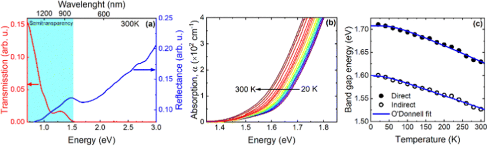 | ||
| Fig. 6 (a) Room temperature transmission and reflection spectra of bulk NiGa2S4. (b) Temperature dependence of the absorption spectra of bulk NiGa2S4 in the vicinity of the absorption edge. (c) Temperature dependence of the indirect and direct energy gap for bulk NiGa2S4 determined from absorption measurements. | ||
The E0(0), S, 〈ℏω〉 fitting parameters are (1.599 ± 0.002) eV, 0.014 ± 0.005, (87.4 ± 0.3) meV and (1.708 ± 0.002) eV, 0.034 ± 0.008, (16.6 ± 0.3) meV for the indirect and direct band gap, respectively. It is worth adding that we did not observe photoluminescence for bulk NiGa2S4, which may additionally confirm that the nature of the energy gap of this crystal is indirect. The indirect nature of the energy gap was reported in the already mentioned theoretical calculations.27 Both the previous and our theoretical calculations show that the difference between the indirect and the direct energy gap is in the order of several dozen meV, which is consistent with the absorption measurements.
20 μl of the exfoliated NiGa2S4 DMF suspension were dropcast onto ITO glass equipped with a mask which set the active area to a spot of 0.196 cm2. The as prepared electrodes were tested in a photoelectrochemical cell featuring a calomel (SCE) electrode and a platinum wire as the reference and counter electrode respectively. A schematic of the PEC cell is illustrated in Fig. S10 (ESI†). The linear sweep voltammetry under pulsed 420 nm light shows a progressive increase of the photoresponse in the interval 0.1–0.5 V vs. SCE. Thus, a potential of 0.5 V vs. SCE. was applied during the tests in the absence or presence of an electron donor, as the material was stable in this range, which is shown by the inherent electrochemistry test reported in Fig. S11 (ESI†). The exfoliated NiGa2S4 flakes deposited in ITO were examined by SEM and presented in Fig. S12 (ESI†) where the 2D nature of the crystals is apparent.
The electrochemical performance of NiGa2S4/ITO electrodes as photodetector systems was tested using LED light with frequencies spanning from the visible to the infrared regions (purple light λ = 420 nm, green light λ = 532 nm, red light λ = 633 nm, deep red light λ = 720 nm, and infrared light λ = 940 nm), both in the presence and in the absence of an electron donor. The chronoamperometric diagrams recorded varying the power of the incident light are reported in Fig. 7 and Fig. 8. Despite its broad absorption in the visible range, the NiGa2S4/ITO photodetector shows a limited photoelectrochemical activity in KOH aqueous solution, characterized by a photocurrent density of 23 μA cm−2 under purple light irradiation (1000 mW) accompanied by a lack of activity for higher irradiation frequencies.
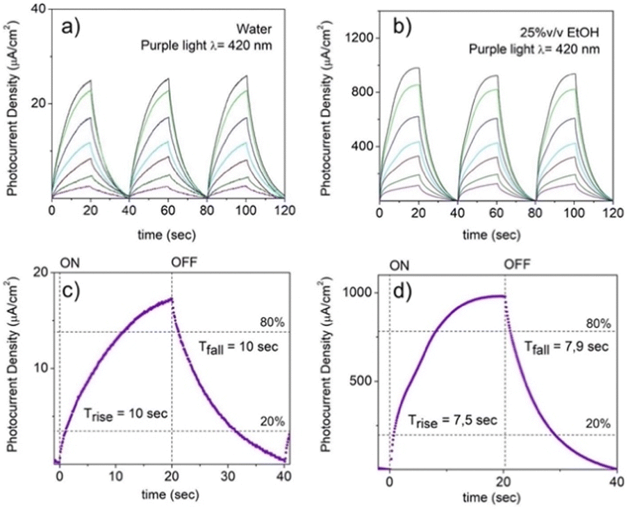 | ||
| Fig. 7 Power dependence of the photocurrent density under the illumination for PEC-type NiGa2S4/ITO photodetector upon purple light (λ = 420 nm) illumination at 0.5 V vs. SCE in (a) aqueous 1 M KOH solution and (b) 1 M KOH ethanol (25% v/v) water solution. The power of the LED source was set to the values of 50 mW (violet), 100 mW (olive), 200 mW (red), 300 mW (cyan), 500 mW (blue), 800 mW (green), and 1000 mW (black). The response time of the PEC photodetector under the illumination of 420 nm LED with a power of 1000 mW is shown in the absence (c) or in the presence (d) of ethanol. | ||
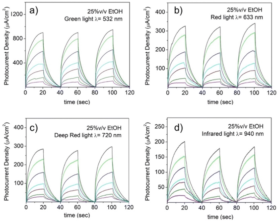 | ||
| Fig. 8 Power dependence of the photocurrent density under the illumination for a PEC-type NiGa2S4/ITO photodetector upon irradiation with (a) green (λ = 532 nm), (b) red (λ = 633 nm), (c) deep red (λ = 720 nm), and (d) infrared (λ = 940 nm) LED sources in 1 M KOH ethanol (25% v/v) water solution at 0.5 V vs. SCE. The power was set to the values of 50 mW (violet), 100 mW (olive), 200 mW (red), 300 mW (cyan), 500 mW (blue), 800 mW (green), and 1000 mW (black). | ||
The response time for purple light irradiation when a 1M KOH aqueous solution is used as the electrolyte is represented in Fig. 10c. Regrettably, the photodetector demonstrates a slow response toward the illumination characterized by a delay of 8 seconds in reaching the 80% of the maximum current density and a recovery time of 10 seconds to restore it to 20 per cent of the values assumed under irradiation.
When a percentage of 25% v/v of ethanol is loaded into the electrolyte solution, the photocurrent displayed by the photodetector upon irradiation with purple light (e.g., 1000 mW) is considerably amplified showing an increase in the current density of a factor ∼40× as shown in Fig. 7b, accompanied by a decrease in the response and a recovery time of ∼25% as can be appreciated by comparing Fig. 7c and d. It is important to notice that the ITO support in the absence of exfoliated NiGa2S4 crystals deposited on it shows a negligible response upon illumination of purple light in the presence of ethanol (Fig. S13, ESI†).
This improvement is attributed to the well-known ability of alcohols to act as an electron donor toward photoexcited semiconductor materials reducing the recombination of photogenerated holes and electrons by reacting with the former.
Photon excitation with an energy larger than the semiconductor material bandgap is able to promote one electron from the semiconductor valence band (VB) to the conduction band (CB), which can subsequently decay to its ground states either by radiative or non-radiative mechanisms. However, in the presence of a sacrificial electron donor with an oxidation potential higher than the semiconductor VB, photogenerated holes (h+) in the VB can be efficiently quenched by the sacrificial electron donor, leaving long-lived electrons in the semiconductor CB, which has been widely exploited in heterogeneous photocatalysis for numerous reactions.32 This ability has been further tested by subjecting the NiGa2S4/ITO photodetector to irradiation with several LED light sources devoid of activity in pure aqueous solution. It is noteworthy that when ethanol is present in the electrolyte solution, a photocurrent is obtained upon irradiation with green, red, deep red and infrared light as shown in Fig. 9. The presence of an electron donor species in solution reveals a new photoresponsive behavior extending the response of the “fueled” NiGa2S4/ITO photodetector over a broad range of frequencies. This trend that can be readily interpreted following the absorption profile of the exfoliated nanosheet crystals, and indicates a continuous absorption over the visible and infrared region (Fig. 5a).
 | ||
Fig. 9 (a) Transient absorption spectra of the NiGa2S4 dispersion in acetonitrile (black) and acetonitrile:ethanol (75![[thin space (1/6-em)]](https://www.rsc.org/images/entities/char_2009.gif) :25, v/v) (red) at 500 ns under a N2 atmosphere upon 420 nm laser excitation. (b) Transient absorption decay of NiGa2S4 dispersion in acetonitrile (black) and acetonitrile:ethanol (75:25, v/v) (red) monitored at 560 nm under a N2 atmosphere upon 420 nm laser excitation. :25, v/v) (red) at 500 ns under a N2 atmosphere upon 420 nm laser excitation. (b) Transient absorption decay of NiGa2S4 dispersion in acetonitrile (black) and acetonitrile:ethanol (75:25, v/v) (red) monitored at 560 nm under a N2 atmosphere upon 420 nm laser excitation. | ||
In analogy with the response in the case of purple light, the presence of ethanol reduces the charge recombination processes typical of excited semiconductor materials by reacting with the photogenerated holes within the crystals, allowing thereby the migration of electrons to the cathode.
In order to further study the effect of ethanol in NiGa2S4 as the photodetector, transient absorption spectroscopy (TAS) experiments have been carried out. The transient absorption spectrum of a NiGa2S4 dispersion in acetonitrile was acquired at 500 ns under a N2 atmosphere and upon 420 nm laser excitation (Fig. 9a). It can be seen that the transient absorption presents a continuous band decreasing in intensity from the UV to the NIR region of the electromagnetic spectrum. Interestingly, the NiGa2S4 transient absorption spectrum in an acetonitrile/ethanol (75:25, v/v) mixture under a N2 atmosphere shows a very similar transient absorption spectrum, although with higher intensity, attributed to photogenerated electrons in the CB. The signal intensity in TAS has been determined to be proportional to the photogenerated charge carrier density,31 and therefore, the higher transient absorption signal can be assigned to an enhanced concentration of electrons in the presence of ethanol. Moreover, the lifetime of the excited states of NiGa2S4 in the presence and absence of ethanol has also been measured, and it is presented in Fig. 9b.
The transient decays of photogenerated electrons in the presence and absence of ethanol present similar bimodal behavior in the range of ns–μs time scale, which can be fitted to a bi-exponential function (eqn (2)).
 | (2) |
The fitting of the experimental data obtained from NiGa2S4 in the absence of ethanol shows a lifetime of 85 ns for the faster component, monitored at 560 nm, while the second decay lifetime is of 639 ns. However, in the presence of ethanol longer lifetimes have been observed, and for the faster component it is 286 ns, while the second decay is 1637 ns. It is worth noticing that the transient absorption decays were monitored at different wavelengths along the measured spectrum, obtaining very similar behavior and lifetimes, indicating that all the observed spectra correspond to the same excited states species.
The longer lifetimes together with the enhanced transient absorption signals in the presence of ethanol can be rationalized by an efficient electron transfer from ethanol to the h+ in the NiGa2S4 VB, leaving a larger population of long-lived e− in the CB, in good agreement with the photocurrent enhancement observed in the PEC measurements.
Figures of merit, such as responsivity and photoresponse, are widely employed to describe photodetector performances, allowing the comparison between systems with different dimensions and architecture.32 The responsivity R expresses the relationship between the photogenerated current obtained under irradiation and the power of the illumination source according to the formula:
| R = Iph/SP(mA W−1) |
| PR = Iph/IOFF |
The responsivity and the photoresponse for the “fueled” NiGa2S4/ITO photodetector are displayed in Fig. 10. The responsivity (Fig. 10a) follows the trend typically observed for a photodetector system characterized by a relative minimum in the high-power regime and a maximum value in the low-power regime, assuming the values of 48.42 mA W−1, 35.54 mA W−1, 11.25 mA W−1, 9.17 mA W−1, and 7.06 mA W−1 for purple (λ = 420 nm), green (λ = 532 nm), red (λ = 420 nm), deep red (λ = 720 nm) and infrared light (λ = 920 nm) respectively. The improvement determined by the presence of ethanol in the electrolyte solution is clearly manifested by the comparison of the values obtained upon irradiation with purple light in aqueous solution, which determines a maximum of responsivity of 0.99 mA W−1. The photoresponse curves displayed in Fig. 10b present a similar trend being characterized by maximum values of 2562, 2431, 894, 778, and 435 for purple (λ = 420 nm), green (λ = 532 nm), red (λ = 420 nm), deep red (λ = 720 nm) and infrared light (λ = 920 nm) respectively and a photoresponsivity of 251 in the case of an “unfueled” NiGa2S4/ITO photodetector.
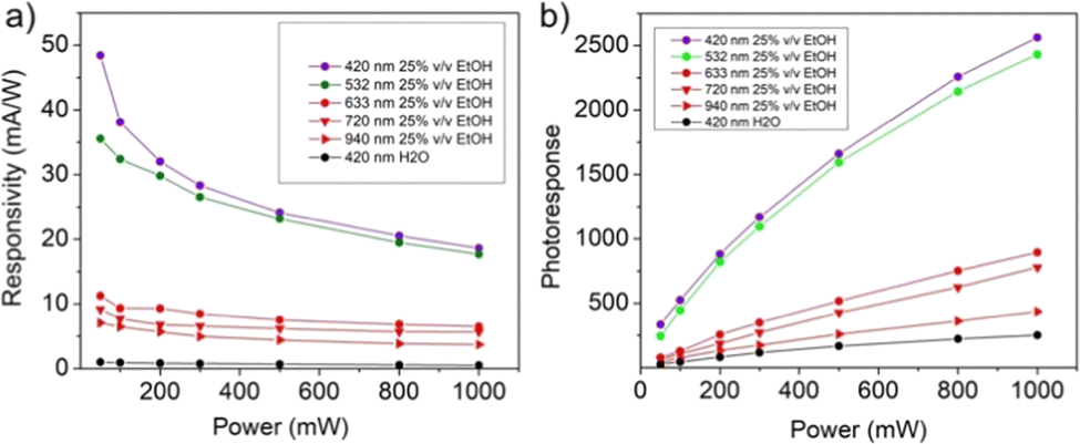 | ||
| Fig. 10 Responsivity (a) and photoresponse (b) for a PEC-type NiGa2S4/ITO photodetector in 1 M KOH ethanol (25% v/v) water solution at 0.5 V vs. SCE. | ||
The values of responsivity obtained for the NiGa2S4/ITO photodetector can be compared with the results reported in the literature for PEC-type photodetectors whose performances are studied in the presence of a comparable applied potential (0–1 V). As shown in Table 1, the values obtained in the present work for the “fueled” NiGa2S4/ITO photodetector exceed those reported for other layered mono-, and ternary-sulfides and perovskite-based systems.
| Materials | Device configuration | Electrolyte | Applied potential | Responsivity (mA W−1) | Wavelength (nm) | Ref. |
|---|---|---|---|---|---|---|
| NiGa2S4 | PEC-type | KOH 1 M ethanol/water | 0.5 V | 48.42 | 420 | This work |
| ZnIn2S4–Ag. Gel–Pt | Metal–Semiconductor–Metal | — | 0 V | 0.02 | Simulated sunlight | 33 |
| InSe nanosheets | PEC-type | 0.2 M KOH | 1 V vs. SCE | 3.3 × 10⁻³ | 455 | 34 |
| 4.0 × 10⁻³ | ||||||
| Black phosphorous nanosheets | PEC-type | 0.1 M KOH | 0 V vs. SCE | 1.9 × 10⁻³ | Simulated sunlight | 35 |
| 2.2 × 10⁻³ | ||||||
| GeSe nanosheets | PEC-type | 0.1 M KOH | 0.3 V | 0.044 | Simulated sunlight | 36 |
| 0.076 | ||||||
| SnS | PEC-type | 0.1 M Na2SO4 | 0.6 | 0.018 | 365 | 21 |
| Perovskite (CH3NH3PbI3) | Metal–semiconductor–metal | — | 5 V | 4.4 | 633 | 37 |
| Perovskite (CH3NH3PbI3) PDPP3T | Metal–semiconductor–metal | — | 1 V | 10.7 | 365 | 38 |
| 25.5 | 650 | |||||
| 5.5 | 937 |
The stability of a photodetector assumes a role of primary importance for the practical application of a device. To address this requirement, long time on-off cycle experiments have been performed investigating the stability of “fueled” NiGa2S4/ITO photodetectors. This evaluation is particularly meaningful considering the presence of a chemical reaction coupled to photodetector cycling, which can cause deactivation due to the presence of oxidation products in solution.
In Fig. S14 (ESI†), the current density obtained under irradiation with purple light (800 mW) and infrared light (300 mW) over a period of 30 minutes is reported. As indicated by the chronoamperometric diagrams the “fueled” NiGa2S4/ITO photodetector shows a stable on-off cycling behavior upon excitation in the maximum of its absorption spectra as well in its minimum, allowing the detection of high-powered visible light and low-powered infrared light signals without a significant decay in the intensity of the signal. To investigate the photoelectrochemical stability in more detail, cyclic voltammetry of the electrode before and after the long-term tests has been performed (Fig. S15, ESI†). The diagrams do not present significant changes after irradiation over a period of 30 minutes, confirming the stability of the NiGa2S4/ITO photodetector under these experimental conditions.
Conclusions
In summary, the activity of a few-layered NiGa2S4/ITO photodetector has been studied highlighting the influence of the ethanol as an electron donor in the reaction media, taking advantage of a well-known resource to reduce the charge recombination in semiconductor-based photocatalysis. The use of ethanol in combination with an ITO-supported layered NiGa2S4 semiconductor demonstrates an unforeseen improvement in this field, able to introduce remarkable amplification of the responsivity (∼×49), photoresponse (∼×10) and spectral response of the device (from 420 to 940 nm). Considering the diffusion of the use of an electron donor species to reduce the electron–hole recombination within a semiconductor material in heterogeneous photocatalysis, it is anticipated that this strategy could be expanded to other semiconductor materials to engineer new high-performance “fueled” photodetector systems.3. Experimental
3.1. Synthesis of bulk NiGa2S4 crystals
Stochiometric amounts of Ni (99.999%, −100 mesh), gallium (99.9999%, granules) and sulfur (99.9999%, granules) corresponding to 15 g of NiGa2S4 were placed in ampoule 35 × 180 mm together with 0.3 g of iodine (99.9%, granules) and sealed under high vacuum. The reaction mixture was first reacted in a muffle furnace at 500 °C for 25 hours, at 600 °C for 50 hours and finally at 800 °C for 50 hours. For the crystal growth by vapor transport the ampoule was placed in a two zone furnace, where the source zone was heated at 850 °C and the growth zone at 800 °C for 10 days. Finally, the crystals were removed from the ampoule in an argon filled glovebox.3.2. Computational methods
The electronic structure calculations were performed using density functional theory with hybrid functionals (HSE6)39 and the projector-augmented wave method as implemented in the MedeA-VASP software package.40 Further calculation parameters were used as follows: plane wave cut-off energy Ecut = 400 eV, energy convergence criterion 1.0 × 10⁻⁵ eV, normal (blocked Davidson) algorithm, requested k-spacing 0.25 Å−1.3.3. Instruments
Scanning electron microscopy: The morphology was investigated using scanning electron microscopy (SEM) with a FEG electron source (Tescan Lyra dual beam microscope). Elemental composition and mapping were performed using an energy dispersive spectroscopy (EDS) analyzer (X-MaxN) with a 20 mm2 SDD detector (Oxford instruments) and AZtecEnergy software. To conduct the measurements, the samples were placed on carbon conductive tape. SEM and SEM-EDS measurements were carried out using a 10 kV electron beam. STEM microscopy was performed with a Tescan Lyra dual beam microscope equipped with an FEG electron source and STEM sample holder. To conduct the measurements, the sample suspension was drop casted on a 200 mesh Cu TEM grid and dried in a vacuum oven (50 °C). STEM measurements were carried out using a 30 kV electron beam.Transmission electron microscopy: aberration-corrected high-resolution (scanning) transmission electron microscopy imaging (HR-(S)TEM) and energy-dispersive X-ray spectroscopy (EDS) were performed using a FEI Titan Cubed Themis microscope (University of Cádiz), which was operated at 80 kV. It was equipped with a double Cs aberration-corrector, a monochromator, an X-FEG gun, an ultrahigh-resolution energy filter (Gatan Quantum ERS), which allows working in dual-EELS mode, and a super-X EDS detector, which consists of four windowless SDD detectors that can be read out independently. HR-STEM imaging was performed using a high-angle annular dark-field (HAADF) detector. EDS quantification was achieved using the Brown–Powell model for the ionization cross sections. Selected Area Electron Diffraction (SAED) and fast Fourier transform (FFT) patterns were automatically indexed using the JEMS software.
Raman spectroscopy: inVia Raman microscope (Renishaw, England) in backscattering geometry with a CCD detector was used for Raman spectroscopy. DPSS laser (532 nm, 50 mW) with an applied power of 5 mW and 50× magnification objective was used for the measurement. Instrument calibration was achieved with a silicon reference which gives a peak position at 520 cm−1 and a resolution of less than 1 cm−1. The samples were suspended in deionized water (1 mg ml−1) and ultrasonicated for 10 min. The suspension was deposited on a small piece of silicon wafer and dried.
Photoelectron spectroscopy: high resolution X-ray photoelectron spectroscopy (XPS) was performed using an ESCAProbeP spectrometer (Omicron Nanotechnology Ltd, Germany) with a monochromatic aluminium X-ray radiation source (1486.7 eV). Wide-scan surveys of all elements were performed, with subsequent high-resolution scans of the C 1s and O 1s. Relative sensitivity factors were used to evaluate the carbon-to-oxygen (C/O) ratios from the survey spectra. The samples were placed on a conductive carrier made from a high purity silver bar. An electron gun was used to eliminate sample charging during measurement (1–5 V).
Electrochemical measurements: The electrochemical characterization by means of cyclic voltammetry was performed using an Autolab PGSTAT 204 (Metroohm, Switzerland). All glassy carbon electrodes were cleaned by polishing with an alumina suspension to renew the electrode surface then washed and wiped dry prior to any use. For the measurements a modified galas carbon electrode was used as the working electrode, and calomel as the reference electrode and platinum counter electrode.
Photo-electrochemical measurements: ITO electrodes were cleaned by rinsing with water, ethanol and acetone and dried at 60 °C. An adhesive mask was applied to reduce the active area to a circle of 0.5 cm in diameter. The samples were dispersed in DMF as the organic solvent to obtain a 1 mg ml−1 suspension. The suspension was then sonicated for 5 min at room temperature before every use. A cleaned ITO electrode was then modified by coating with a 10 μL aliquot of the suspension and left to dry in a box oven at 60 °C to prepare MnIn2Se4/ITO electrodes. The modified GC electrodes, SCE reference electrode, and platinum counter electrode were then placed into an electrochemical cell which contains the electrolyte solution, and the measurements were then taken. All measurements were taken for three consecutive scans at a scan rate of 100 mV s−1.
UV-Vis: the samples were illuminated by a halogen lamp and the reflected or transmitted light was dispersed utilizing a 0.55 m focal length single-grating monochromator. The measurements were performed using a lock-in technique. The PbS and Si photodiodes were used to detect the NIR and VIS signal, respectively.
Author contributions
The manuscript was written through the contributions of all authors. All authors have given approval to the final version of the manuscript.Conflicts of interest
The authors declare no competing financial interest.Acknowledgements
This project was supported by ERC-CZ program (project LL2101) from Ministry of Education Youth and Sports (MEYS). L. L. acknowledges funding from the Andalusian regional government (FEDER-UCA-18-106613), the European Union's Horizon 2020 research and innovation program (grant agreement 823717 – ESTEEM3), the Spanish Ministerio de Economia y Competitividad (PID2019-107578GA-I00), and the Ministerio de Ciencia e Innovación MCIN/AEI/10.13039/501100011033, and the European Union “NextGenerationEU”/PRTR (RYC2021-033764-I, CPP2021-008986). The (S)TEM measurements were performed at the National Facility ELECMI ICTS (“Division de Microscopia Electronica”, Universidad de Cadiz, DME-UCA).References
- Y. Li, Z. Li, C. Chi, H. Shanm, L. Zheng and Z. Fang, Adv. Sci., 2017, 4, 1600430 CrossRef PubMed.
- I. P. Choudhuri, P. Bhauriyal and B. Pathak, Chem. Mater., 2019, 31, 8260–8285 CrossRef CAS.
- Y. Zhu, L. Peng, Z. Fang, C. Yan, X. Zhang and G. Yu, Adv. Mater., 2018, 30, 1706347 CrossRef PubMed.
- D. L. Duong, S. J. Yun and Y. Lee, ACS Nano, 2017, 11, 11803–11830 CrossRef CAS PubMed.
- (a) N. Perea-López, A. L. Elías, A. Berkdemir, A. Castro-Beltrán, H. R. Gutiérrez, S. Feng, T. HayashI, F. López-Urías, S. Ghosh, B. Muchharla, S. Talapatra and H. Terrones, Adv. Funct. Mater., 2013, 5517 Search PubMed; (b) C. Chunxiao, S. Jingzhi, W. Yanlong and Y. Ting, Adv. Optical Mater., 2017, 1700767 Search PubMed; (c) L. Jingyang, H. Jianfu, H. Hongxing, F. Xiaoyan and H. Kai, Mat. Sci Semicon. Proc., 2020, 107, 104804–104807 CrossRef; (d) H. Nengjie, K. Jun, W. Zhongming, W. Shu-Shen, L. Jingbo and W. Su-Huai, Adv. Funct. Mater., 2014, 7031 Search PubMed; (e) G. A. Muller, J. B. Cook, H. S. Kim, S. H. Tolbert and B. Dunn, Nano Lett., 2015, 15, 1907–1911 CrossRef PubMed; (f) D. Wu, M. Xu, L. Zeng, Z. Shi, Y. Tian, X. J. Li, C.-X. Shan and J. Jie, ACS Nano, 2022, 16, 5545–5555 CrossRef CAS PubMed; (g) D. Wu, J. Guo, C. Wang, X. Ren, Y. Chen, P. Lin, L. Zeng, Z. Shi, X. L. Li, C.-X. Shan and J. Jie, ACS Nano, 2021, 15, 10119–10129 CrossRef CAS PubMed; (h) D. Wu, J. Guo, J. Du, C. Xia, L. Zeng, Y. Tian, Z. Shi, Y. Tian, X. J. Li, Y. H. Tsang and J. Jie, ACS Nano, 2019, 9, 9907–9917 CrossRef PubMed; (i) D. Wu, C. Guo, L. Zeng, X. Ren, Z. Shi, L. Wen, Q. Chen, M. Zhang, X. J. Li, C.-X. Shan and J. Jie, Light. Sci. Appl., 2023, 5, 12 Search PubMed; (j) D. Wu, R. Tian, P. Lin, Z. Shi, X. Chen, M. Jia, Y. Tian, X. Li, L. Zeng and J. Jie, Nano Energy, 2022, 104, 107972 CrossRef CAS.
- S. Lei, L. Ge, Z. Liu, S. Najmaei, G. Shi, G. You, J. Lou, R. Vajtai and P. M. Ajayan, Nano Lett., 2013, 13, 2777–2781 CrossRef CAS PubMed.
- J. D. Yao, Z. Q. Zheng, J. M. Shaoa, J. Yang and G. W. Stable, Nanoscale, 2015, 7, 14971–14974 Search PubMed.
- W. Huang, L. Gan, H. Yang, N. Zhou, R. Wang, W. Wu, H. Li, Y. Ma, H. Zeng and T. Zhai, Adv. Funct. Mater., 2017, 27, 1702448 CrossRef.
- T. Maeda, W. Y. Gong and T. Wada, Jpn. J. Appl. Phys., 2016, 55, 04ES15-1-04e5-1510 Search PubMed.
- (a) J. Shi, T. F. T. Cerqueira, W. Cui, F. Nogueira, S. Botti and M. A. L. Marques, Sci. Rep., 2017, 7, 43179 CrossRef PubMed; (b) K. Pal, Y. Xia, J. Shen, J. He, Y. Luo, M. G. Kanatzidis and C. Wolverton, npj Comput. Mater., 2021, 7, 2368 Search PubMed.
- C. Razzetti, P. P. Lottici and G. Antonioli, Prog. Cryst. Growth Charact., 1987, 15, 43–73 CrossRef.
- K. J. Z. Range, Naturforsch, 1996, 51, 12631264 Search PubMed.
- S. A. Lopez-Rivera, A. J. Mora, D. Acosta Najarro, A. V. Rivera and R. Avila Godoy, Semicond. Sci. Technol., 2001, 16, 367–371 CrossRef CAS.
- (a) G. Zhang, H. Wu, D. Chen, N. Li, Q. Xu, H. Li and J. He, Green Energy Environ., 2022, 7, 176 CrossRef CAS; (b) J. Wang, S. Sun, R. Zhou, Y. Li, Z. He, H. Ding and D. Chen, Adv. Funct. Mater., 2017, 27, 1702448 CrossRef; (c) M. Yuan, M. Gong, H. Huang, Y. Zhao, Y. Ying and S. Wang, Inorg. Chem. Front., 2022, 9, 5725–5734 RSC; (d) L. Shi, P. Yin and Y. Dai, Langmuir, 2013, 29, 12818–12822 CrossRef CAS; (e) T. Liu, L. Wang, X. Liu, C. Sun, Y. Lev, R. Miao and X. Wang, Chem. Eng. J., 2020, 379, 1223792 Search PubMed; (f) M. Hao, X. Deng, L. Xu and L. Zhaohui, App. Cat. B: Environ., 2019, 252, 18 CrossRef CAS; (g) L. Guo, X. Han, K. Zhang, Y. Zhang, Q. Zhao, D. Wang and F. Fu, Catalysts, 2019, 9, 729–736 CrossRef CAS; (h) Z. Lei, W. You, M. Liu, G. Zhou, T. Takata, M. Hara, K. Domen and C. Li, Chem. Commun., 2003, 2142–2143 RSC; (i) F. Xing, Q. Liu and C. Huang, Sol. RRL, 2020, 4, 1900483 CrossRef CAS; (j) X. Jiao, Z. Chen, X. Li, Y. Sun, S. Gao, W. Yan, C. Wang, Q. Zhang, Y. Lin, Y. Luo and X. Xie, J. Am. Chem. Soc., 2017, 139, 75867594 Search PubMed; (k) S. Wang, B. Y. Guan, Y. Lu and X. W. Lou “David”, J. Am. Chem. Soc., 2017, 139, 17305–17308 CrossRef CAS PubMed.
- L. Valdman, V. Mazanek, P. Marvan, M. Serra, R. Arenal and Z. Sofer, Adv. Opt. Mater., 2021, 9, 2100845 CrossRef CAS.
- J. Wei, C. Wang, T. Zhang, C. M. Dai and S. Chen, Nanoscale, 2019, 11, 13924 RSC.
- (a) A. Yaouanc, P. Dalmas de Réotier, Y. Chapuis, C. Marin, G. Lapertot, A. Cervellino and A. Amato, Phys. Rev. B: Condens. Matter Mater. Phys., 2008, 77, 092403 CrossRef; (b) Y. Nambu and S. J. Nakatsuji, J. Phys. Condens. Matter, 2011, 23, 164202 CrossRef; (c) D. E. MacLaughlin, Y. Nambu, S. Nakatsuji, R. H. Heffner, L. Shu, O. O. Bernal and K. Ishida, Phys. Rev. B: Condens. Matter Mater. Phys., 2008, 78, 220403 CrossRef.
- (a) A. M. Zardkhousi and S. S. H. Davarani, J. Colloid Interface Sci., 2019, 535, 195 CrossRef PubMed; (b) S. Liu, K. H. Kim, J. M. Yun, A. Kundu, K. Vijaya, U. M. Patil, C. Ray and S. C. Jun, J. Mater. Chem. A, 2017, 5, 6292–6298 RSC.
- S. Chen, C. Teng, M. Zhang, Y. Li, D. Xie and G. Shi, Adv. Mater., 2016, 28, 5969–5974 CrossRef CAS PubMed.
- W. Wang, Y. Zhang, Y. Gao, P. Luo, J. Su, W. Han, K. Liu, H. Li and T. Zhai, Small, 2019, 15, 1901347 CrossRef PubMed.
- W. Huang, Z. Xie, T. Fan, J. Li, Y. Wang, L. Wu, D. Ma, Z. Li, Y. Ge, Z. N. Huang, X. Dai, Y. Xiang, J. Li, X. Zhu and H. Zhang, J. Mater. Chem. C., 2018, 6, 9582–9593 RSC.
- N. Fajrina and M. Tahir, Int. J. Hydrogen Energy, 2019, 44, 540–578 CrossRef CAS.
- T. M. McCormick, B. D. Calitree, A. Orchard, N. D. Kraut, F. V. Bright, M. R. Detty and R. Einsenberg, J. Am. Chem. Soc., 2010, 132(44), 15480–15483 CrossRef CAS PubMed.
- M. P. Pardo, M. F. Gardette, M. Wintenberger and M. Guittard, Mater. Res. Bull., 1991, 26, 295–299 CrossRef CAS.
- M. E. Valentine, T. Higo, Y. Nambu, D. Chaudhuri, J. Wen, C. Broholm, S. Nakatsuji and N. Drichko, Phys. Rev. Lett., 2020, 125, 197201 CrossRef CAS PubMed.
- Materials data on Material Project mp-6959 (https://materialsproject.org/materials/mp6959?chemsys=Ni-Ga-S).
- K. Z. Rushchanskii, H. Haeuseler and D. M. Bercha, J. Phys. Chem. Solids, 2002, 63, 2019–2028 CrossRef CAS.
- I. Vurgaftman, J. R. Meyer and L. R. Ram-Mohan, J. Appl. Phys., 2001, 89, 5815–5862 CrossRef CAS.
- J. Kopaczek, S. Zelewski, K. Yumigeta, R. Sailus, S. Tongay and R. Kudrawiec, J. Phys. Chem. C, 2022, 126(12), 5665–5674 CrossRef CAS PubMed.
- K. P. O’Donnell and X. Chen, Appl. Phys. Lett., 1991, 58, 2924–2927 CrossRef.
- A. Maurano, C. G. Shuttle, R. Hamilton, A. M. Ballantyne, J. Nelson, W. Zhang, M. Heeney and J. R. Durrant, J. Phys. Chem. C, 2011, 115, 5947–5957 CrossRef CAS.
- S. J. Van Enk, J. Phys. Commun., 2017, 1, 045001 CrossRef.
- L. Mandal, N. S. Chaudhari and S. Ogale, ACS Appl. Mater. Interfaces, 2013, 9141–9147 CrossRef CAS PubMed.
- Z. Li, H. Qiao, Z. Guo, X. Ren, Z. Huang, X. Qi, S. C. Dhanabalan, J. S. Ponraj, D. Zhang, J. Li, J. Zhao, J. Zhong and H. Zhang, Adv. Funct. Mater., 2018, 28, 1705237 CrossRef.
- X. Ren, Z. Li, Z. Huang, D. Sang, H. Qiao, X. Qi, J. Li, Z. Zhong and H. Zhang, Adv. Funct. Mater., 2017, 27, 1606834 CrossRef.
- D. Ma, J. Zhao, R. Wang, C. Xing, Z. Li, W. Huang, X. Jiang, Z. Guo, Z. Luo, Y. Li, J. Li, S. Luo, Y. Zhang and H. Zhang, ACS Appl. Mater. Interfaces, 2019, 11, 4278–4287 CrossRef CAS PubMed.
- H. Fang, J. Li, Y. Sun, Q. Li, J.-L. Sun, L. Wang and Q. Yan, ACS Appl. Mater. Interfaces, 2017, 9, 10921–10928 CrossRef CAS PubMed.
- S. Chem, C. Teng, M. Zhang, Y. Li, D. Xie and G. Shi, Adv. Mater., 2016, 28, 5969–5974 CrossRef PubMed.
- J. Heyd, G. E. Scuseria and M. Ernzerhof, J. Chem. Phys., 2003, 118, 8207–8215 CrossRef CAS.
- G. Kresse and J. Furthmüller, Phys. Rev. B: Condens. Matter Mater. Phys., 1996, 54, 11169–11186 CrossRef CAS PubMed.
Footnote |
| † Electronic supplementary information (ESI) available. See DOI: https://doi.org/10.1039/d3tc00508a |
| This journal is © The Royal Society of Chemistry 2023 |