
 Open Access Article
 This Open Access Article is licensed under a Creative Commons Attribution-Non Commercial 3.0 Unported Licence
Transition-metal phosphors with emission peak maximum on and beyond the visible spectral boundaries
Guowei
Ni
a,
Jie
Yan
b,
Yixin
Wu
b,
Fan
Zhou
b,
Pi-Tai
Chou
 *c and
Yun
Chi
*ab
*c and
Yun
Chi
*ab
aDepartment of Chemistry, City University of Hong Kong, Kowloon Tong 999077, Hong Kong SAR, China
bDepartment of Materials Sciences and Engineering, and Center of Super-Diamond and Advanced Films (COSDAF), City University of Hong Kong, Kowloon Tong 999077, Hong Kong SAR, China. E-mail: yunchi@cityu.edu.hk
cDepartment of Chemistry, Taiwan University, Taipei 10617, Taiwan, China. E-mail: chop@ntu.edu.tw
First published on 7th February 2023
Abstract
Third-row transition-metal complexes remain a key component in the preparation of light-emitting layers for future OLED technology. Hence, it is of utmost importance to expand their emission peak wavelengths into the true-blue (∼460–470 nm) and near-infrared (NIR) regions (∼700–1000 nm). Stable true-blue phosphors are expected to excel in commercially available lighting luminaries and visual devices, such as displays and monitors, while efficient NIR emitters will enable new applications such as sensing, imaging, and optical communication. In theory, these advanced emitters can be assembled using transition metals such as iridium and platinum and judiciously designed chelates, as elaborated in this chemistry frontier article.
Introduction
Organic light-emitting diodes (OLED) are particularly useful in the fabrication of full color display panels and various lighting luminaries. Typical OLED is expected to generate 25% singlet exciton and 75% triplet exciton during operation. According to this 1![[thin space (1/6-em)]](https://www.rsc.org/images/entities/char_2009.gif) :3 spin statistics, fluorescent materials are only capable of achieving the internal quantum efficiency (ηint) of 25%, which is defined as the ratio of emitted photons that can be extracted from the total injected carriers (or theoretical electron spin statistics) and, hence, cannot actively serve as adequate OLED emitters. To circumvent this deficiency, both phosphorescent and thermally activated delayed fluorescence (TADF) emitters were employed to replace the inferior fluorescent emitters. On the one hand, the third-row transition metal complexes, due to their better stability and efficient spin–orbit coupling induced by their central metal ion, to a large extent, would effectively remove the spin-forbidden nature of the intersystem crossing between singlet and triplet excitons, resulting in an essentially unitary ηint and bright electroluminescence.1 On the other hand, TADF emitters take advantage of the significantly reduced energy gap, ΔEST, between singlet and triplet excited states; hence, the faster forward (ISC) and reverse intersystem crossing (RISC) result in efficient utilization of inaccessible triplet exciton back to the emitting singlet excited state. In theory, ηint of TADF emitters may also reach as high as 100%. Nowadays, both classes of emitters compete for practical industrial applications.
:3 spin statistics, fluorescent materials are only capable of achieving the internal quantum efficiency (ηint) of 25%, which is defined as the ratio of emitted photons that can be extracted from the total injected carriers (or theoretical electron spin statistics) and, hence, cannot actively serve as adequate OLED emitters. To circumvent this deficiency, both phosphorescent and thermally activated delayed fluorescence (TADF) emitters were employed to replace the inferior fluorescent emitters. On the one hand, the third-row transition metal complexes, due to their better stability and efficient spin–orbit coupling induced by their central metal ion, to a large extent, would effectively remove the spin-forbidden nature of the intersystem crossing between singlet and triplet excitons, resulting in an essentially unitary ηint and bright electroluminescence.1 On the other hand, TADF emitters take advantage of the significantly reduced energy gap, ΔEST, between singlet and triplet excited states; hence, the faster forward (ISC) and reverse intersystem crossing (RISC) result in efficient utilization of inaccessible triplet exciton back to the emitting singlet excited state. In theory, ηint of TADF emitters may also reach as high as 100%. Nowadays, both classes of emitters compete for practical industrial applications.
As for the phosphorescence emitters, the Ir(III) based metal complexes have been employed as the commercially viable red and green OLED phosphors. However, currently, virtually no true-blue Ir(III) phosphors are capable of affording both high efficiency and stability in devices, retarding their application en route to commercial applications.2 These deficiencies encourage intensive and wide investigations on the blue emissive Ir(III) phosphors, particularly the carbene-based Ir(III) complexes,3 as this class of emitters is expected to be more versatile in chemical designs and superior physical properties and efficiencies in comparison to those with Pt(II), Au(I), and Au(III) metal atoms.
Recently, both technologies termed “hyperfluorescence”4,5 and “hyperphosphorescence”6 (also known as the phosphor sensitized fluorescence)7 have gained particular attention for the fabrication of efficient and durable blue emissive OLED devices. Their basic principle is to effectively harvest triplet excitons by TADF emitters or transition metal phosphors, which then undergo rapid Förster resonance energy transfer to blue organoboron TADF emitters having fast fluorescent lifetimes and narrow emission bandwidths mainly due to the multi-resonance effect.8 This process partly solves the deadlock on inadequate efficiency and poor durability of true-blue OLED devices, with emission peak maximum located at ∼460–470 nm. Concurrently, their narrowband blue emission matches well the BT.2020 color standard for ultra-HD projectors and televisions. Relevant endeavor is timely, which will surely impact the future development of blue OLED devices, emphasizing both efficiency and durability. With appropriate structural modification, Ir(III) sensitized hyperphosphorescence may outperform the TADF sensitized hyperfluorescence due to the partially allowed intersystem crossing and thus better utilization of triplet excitons.
In yet another approach, near-infrared (NIR) irradiation with a peak wavelength spanning 700–1000 nm region is invisible to human eyes and cannot be employed for the fabrication of visual accessories.9 Alternatively, it possesses an increased penetration depth into the human flesh, and the corresponding OLED devices worn by patients are expected to be pivotal for emerging applications such as sensing, imaging, phototherapy, and hence the fabrication of pulse oximeter and photoplethysmography.10,11 As efficient NIR phosphors, Pt(II) complexes possess a d8-electron configuration and exhibit square-planar geometries. They are in sharp contrast to Ir(III) and Os(II) metal complexes, where they possess a distinctive d6-electron configuration with octahedral geometry.12 It should be noted that in the octahedral complexes, the surrounding chelates provide effective steric shielding against the formation of any direct metal–metal contact. Differently, the square-planar Pt(II) complexes would facilitate face-to-face stacking between adjacent Pt(II) metal units, leading to intimate Pt⋯Pt and/or π⋯π interactions.13,14 This linearly arranged aggregate would exert a strong influence on their photophysical properties, i.e., giving metal–metal-to-ligand charge transfer (MMLCT) or even excimeric ππ* transition, rather than the combined ligand-centered ππ* and metal-to-ligand charge transfer (MLCT) characteristics. Emission originating from the MMLCT transition process is typically much red shifted with respect to the “isolated” monomers that exist in dilute solution, dispersed polymer matrix, or co-deposited thin film. Hence, the monomeric Pt(II) complexes with sky-blue and green emissions may become NIR emitters when self-assembled, thus opening the gateway to efficient NIR OLEDs.
Hence, we will use this frontier article to discuss the fundamental insights into these true-blue and NIR emissive Ir(III) and Pt(II) phosphors, together with their potential impacts on the future development of relevant OLED devices. Moreover, both classes of emitters, synthetically, were constructed using distinctive chelates and metal elements, which are judiciously selected for achieving optimal structural and photophysical properties. Thus, critical comments will also be provided on the pros and cons of their designs and perspectives so that readers can gain an in-depth understanding, beneficial for future development.
True-blue emitters
There are two possible classes of Ir(III) complexes suitable for efficient blue emission. One involves functional cyclometalates linked to the N-donor fragment, such as pyridine, pyrazole, or imidazole, in the form of either homoleptic Ir(C^N)3 or heteroleptic Ir(C^N)2(L^X) architectures, where C^N denotes the N-containing aromatics and L^X specifies the anionic ancillary.15–17 The alternatives are carbene complexes f-Ir(C^C)3 and m-Ir(C^C)3,18–21 where f- and m- indicate facial and meridional orientation, respectively. Their proposed energy diagrams are depicted in Scheme 1. The most well-known examples of Ir(III) based pyridine and carbene-containing complexes are sky-blue bis[2-(4,6-difluorophenyl)pyridinato-C2,N](picolinato)iridium(III) (FIrpic)22 and purple emitting tris(1-phenyl-3-methylbenzimidazolin-2-ylidene-C,C2′)iridium(III), [Ir(pmb)3],23 for which the ground state (S0), lowest energy triplet excited state (T1), and upper lying metal-centered (MC) dd excited state are indicated in black, dotted blue, and red traces, respectively. The T1 excited state of both complexes constitutes a mixed ligand-centered ππ* and MLCT transition, while the high-lying MC dd state involves a T1 state geometry with metal–ligand distances lengthened, i.e., an activated radiationless state close to the T1 excited state.24 The Ir(C^C)3 complexes exhibit more destabilized T1 and MC dd excited states than those of Ir(C^N)3 and Ir(C^N)2(L^X) due to the high-lying π* orbital of carbene fragments and stronger Ir–C bonding interaction. With this in mind, tuning emission from sky-blue FIrpic and analogues to true-blue color can be done by destabilizing the T1 state, i.e., the addition of electron-withdrawing (or donating) group at the HOMO (or LUMO) segment of Ir(III) complexes, to which the newly obtained T1 state, i.e., T1′ state, is now indicated in blue solid line (Scheme 1(a)). Accordingly, this manipulation is expected to reduce the T1′-MC dd energy gap (ΔE), inducing a faster emission quenching. Conversely, tuning emission from purple [Ir(pmb)3] and derivatives to true-blue required stabilization of the T1 state via the addition of electron-deficient substituent(s) at the carbene entity, resulting in the increase of ΔE (see Scheme 1(b)). The enlarged T1′-MC dd energy gap would retard the non-radiative decay process, making them one of the best candidates for showing both efficient and durable blue emission.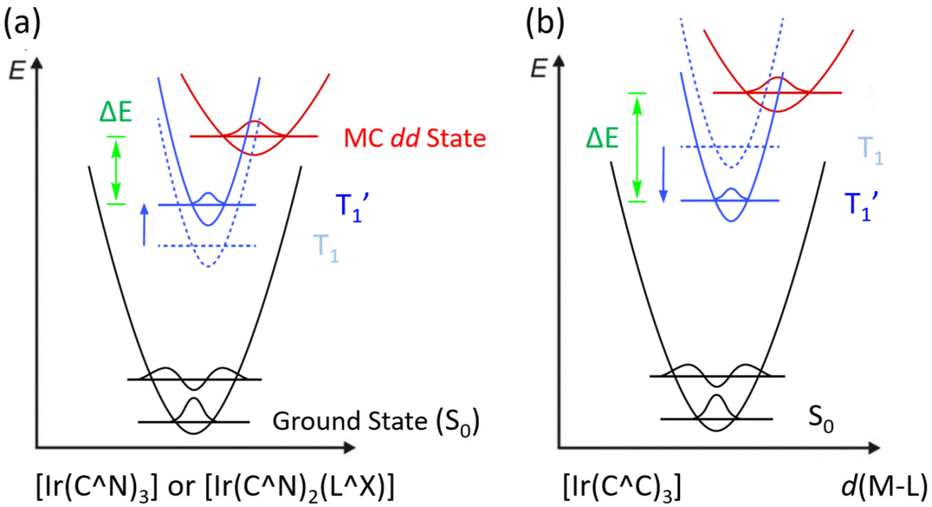 | ||
| Scheme 1 Potential energy surface diagrams for hypothetical Ir(III) complexes with either pyridine (a) or carbene-based cyclometalates (b) and strategic approach in obtaining blue emission; definition of T1 and T1′ states is elaborated in the text. | ||
Practically, tuning emission to blue can be easily achieved according to the aforementioned strategies. Scheme 2 depicts the structures of parent carbene pro-chelates (pmi)H+,23 (tfpmi)H+,25 and (pmb)H+,23 together with a series of functional derivatives with an aim to reduce the T1′-MC dd energy gap. Chemically, this can be done via the addition of electron-deficient substituent(s) to the carbene fragment or, alternatively, extending the π-conjugation of carbene at the N-aryl site as the less effective methodology.
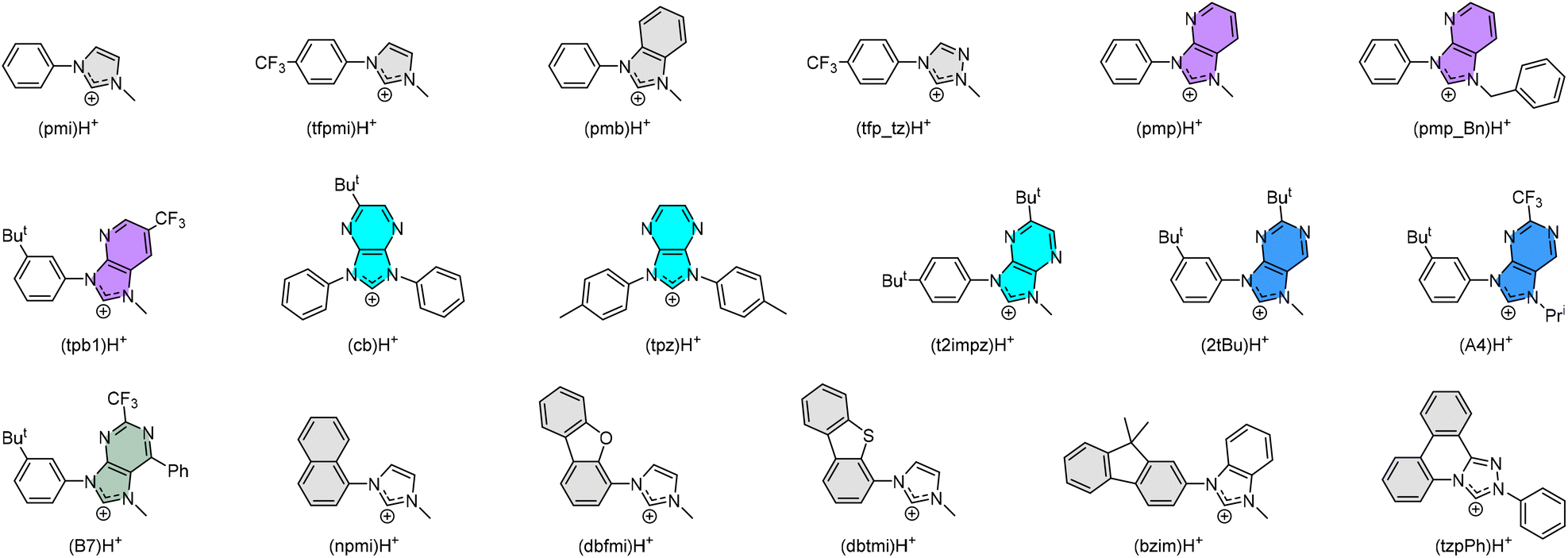 | ||
| Scheme 2 Some representative carbene cyclometalates employed in the preparation of homoleptic Ir(III) metal complexes. | ||
The positive effects on Ir(III) complexes with electron-deficient carbene can be comprehended as follows: (i) Carbene complexes [Ir(pmb)3] with m- and f-arranged benzo[d]imidazolylidene chelates exhibit ultraviolet emission at λmax = 389 nm and 395 nm, and radiative lifetimes of 5.5 and 7.5 μs in degassed solution at RT,23,26 whereas the corresponding imidazo[4,5-b]pyridin-2-ylidene complexes m-[Ir(pmp)3] and f-[Ir(pmp)3]27 gave better emission at λmax = 465 nm and 418 nm and much shorter radiative lifetimes of 1.58 and 1.03 μs, respectively. (ii) Carbene complex f-[Ir(cb)3] with imidazo[4,5-b]pyrazin-2-ylidene chelates displays emission at 456 nm in toluene with a high quantum yield of 88% and radiative lifetime of 0.47 μs in polystyrene matrix at 1 wt%.28 Despite being a mixture of isomers, f-[Ir(cb)3] has been successfully used in the fabrication of blue OLED devices with high efficiency and steadily improved device lifespans.29,30 This is in agreement with the high chemical stability of an analogue f-Ir(tpz)3 in the solid state.31 (iii) In sharp contrast to the Ir(III) complexes with electron-deficient carbene chelates such as (pmp_Bn)H+,32 (tpb1)H+,33 (t2impz)H+,34 (2tBu)H+,35 (A4)H+,36 and (B7)H+,36 those with extended π-conjugation, i.e., (npmi)H+,37 (dbfmi)H+,38 (dbtmi)H+,39,40 (bzmi)H+,41 and even (tzpPh)H+,42 can only afford Ir(III) complexes having structured emission, long radiative lifetime, and relatively poor quantum yield, the latter of which points out the inferiority of the associated designs. (iv) Homoleptic Ir(III) carbene emitters with electron-deficient carbene chelates, i.e., (tfp_tz)H+,43 and others have all been adequately tested in giving prominent blue hyperphosphorescence, where the device longevity is still at the top of the agenda and needs improvement. So far, one such carbene emitter had already achieved both high efficiency and long device lifetime of LT50 of 431 h for an initial brightness of 500 cd m−2,44 confirming their potential as desirable blue emitters.
Near-infrared emitters
Maximizing possible Pt⋯Pt stacking in the solid state should be one of the most promising strategies in inducing the red-shifted emission, and hence, we proceeded to synthesize representative Pt(II) metal complexes, namely: Pt(fppz)2,45,46 Pt(fprpz)2,47 (4H),48 (DR), and (Per-DR),49 as shown in Scheme 3. It is notable that all of them possess the electron-deficient 3-trifluoromethyl pyrazolyl and pyrimidinyl coordination fragments, to which the pyrimidinyl fragment offered further red-shifted emission attributed to the stronger Pt–C covalent interaction. Also, the uncoordinated N-atom of these fragments is expected to foster two inter-chelate N⋯H–C hydrogen bonding, giving nearly planar coordination geometry.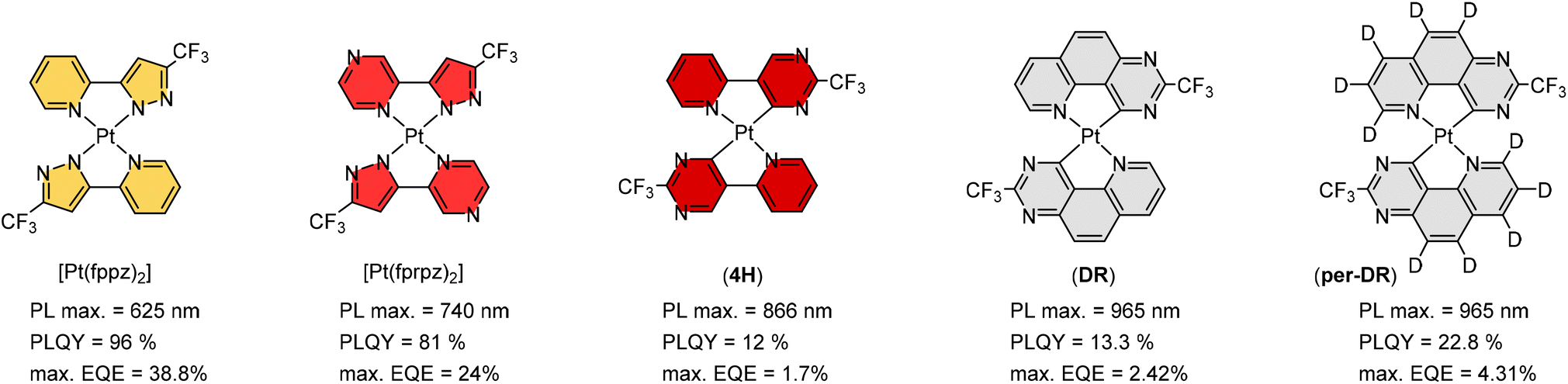 | ||
| Scheme 3 Representative Pt(II) complexes showing strong solid-state aggregation and efficient emissions in saturated red and NIR regions. | ||
Moreover, the electron deficiency of chelates would pass to the central Pt(II) atom, allowing the easy formation of Pt⋯Pt interaction (for sharing their electrons) in the solid state upon grinding or forming a thin film via thermal vapor deposition. In contrast, disruption of Pt⋯Pt stacking can be achieved by replacement of CF3 substituents of Pt(fppz)2 or Pt(fprpz)2 with electron-donating methyl or tert-butyl substituent.45 The increased electron richness turned corresponding Pt(II) complexes from sparing soluble to highly soluble in common organic solvents at RT and afforded typical MLCT + ππ* transition characteristics. In sharp contrast, the electron-deficient Pt(II) complexes (i.e., those depicted in Scheme 3) exhibited higher energy emission in diluted and degassed solution at RT or upon co-deposition with host material or inert media in a doped thin film,50 indicating the prohibition of Pt⋯Pt interaction. Such a remarkable photophysical behavior can be explained using two potential energy diagrams shown in Scheme 4.
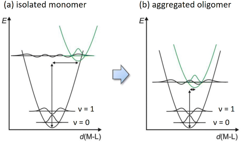 | ||
| Scheme 4 Schematic potential energy diagrams for square planar Pt(II) emitters (a) as isolated molecules and (b) after aggregation and formation of intimate Pt⋯Pt interaction. | ||
Hence, as isolated single molecules, their excited state structures are expected to be significantly different from that of the ground state (i.e., greater deviation in d(M–L)). Consequently, it causes a significant displacement of the equilibrium distance in the corresponding potential energy curve, as shown in Scheme 4a. However, upon the formation of aggregated oligomers, the excited state characteristics are now dominated by the MMLCT transition, which lowered the potential energy of the excited state in comparison to that of the monomer. The energy gap of aggregated Pt(II) complexes is thus reduced, most likely to the NIR region, depending on the chelate design. Moreover, the generated exciton will be delocalized along the aligned molecules upon excitation, where the associated vibration modes will be evenly partitioned over all effective stacked molecules, i.e., the N number involved in the exciton delocalization. Theoretically, this is equivalent to reducing the vibrational reorganization energy from λ of the monomeric complex to λ/N in the N exciton delocalization, producing a less displaced excited-state potential energy surface (PES) with respect to the PES of the ground state (see Scheme 4b).48 The delocalized exciton, therefore, results in the exciton-vibration decoupling that reduces the rate of internal conversion, which virtually bypasses the radiationless quenching imposed by the energy gap law. The net result is the generation of efficient NIR emission, leading to all Pt(II) complexes depicted in Scheme 3 exhibiting very high emission efficiencies at peak wavelengths beyond 700 nm and approaching the NIR II region starting from 1000 nm.
Finally, for further minimization of exciton–vibration coupled deactivations, we executed the H–D substitution of Pt(II) derivative DR for reducing the high-frequency C–H vibrations, where the difference in energy between C–H and C–D promoting stretch modes is ∼800 cm−1. Therefore, for the C–D substituted Pt(II) complexes, according to the energy gap law, upon electronic-vibrational (C–D stretching) coupling, the accepting vibrational modes, such as those C![[double bond, length as m-dash]](https://www.rsc.org/images/entities/char_e001.gif) C vibrations associated with ππ* transition or d(M–L) changed vibration associated with MLCT, required higher quanta to match the energy gap than that of the C–H complexes. Therefore, the C–D complexes are subject to a lower internal conversion rate than the corresponding C–H analogues, especially in the NIR region. This operation is nontrivial and requires a multi-step synthetic protocol. Worth all the effects, photoluminescence with max. at ∼1000 nm and quantum yield of 23 ± 0.3% was obtained for the fully deuterated Pt(II) derivative Per-DR.49 In addition to the improved photophysical data, the respective NIR OLED device gave a peak wavelength of 995 nm, maximum external quantum efficiency (max. EQE) of 4.31%, and radiance of 1.55 W Sr−1 m−2 at 10 mA cm−2, marking a new milestone for the studies.
C vibrations associated with ππ* transition or d(M–L) changed vibration associated with MLCT, required higher quanta to match the energy gap than that of the C–H complexes. Therefore, the C–D complexes are subject to a lower internal conversion rate than the corresponding C–H analogues, especially in the NIR region. This operation is nontrivial and requires a multi-step synthetic protocol. Worth all the effects, photoluminescence with max. at ∼1000 nm and quantum yield of 23 ± 0.3% was obtained for the fully deuterated Pt(II) derivative Per-DR.49 In addition to the improved photophysical data, the respective NIR OLED device gave a peak wavelength of 995 nm, maximum external quantum efficiency (max. EQE) of 4.31%, and radiance of 1.55 W Sr−1 m−2 at 10 mA cm−2, marking a new milestone for the studies.
Challenges and future perspectives
Several challenges need to be solved before efficient and durable true-blue and NIR-emitting OLED devices can be utilized for possible commercial applications. As to the true-blue phosphors, according to our analysis, homoleptic Ir(III) carbene complexes should outperform their N-donor counterparts in terms of operational stability, attributed to the increased ligand–metal bond strength. Moreover, Ir(III) emitters are more stable than the Au(I) and Cu(I) based blue emitters;51,52 the latter possess only the monodentate ligands, of which their ligand–metal bond strength should be less robust than the bidentate bonding in the Ir(III) complexes. Under similar criteria, the bidentate metal-chelate interaction of Ir(III) based emitters is also less stable than that of the tetradentate coordinative Pt(II) based blue emitters,53 but the latter suffers from longer radiative lifetimes due to the diminished total zero-field splitting (ΔE(ZFS)) of the emitting triplet state.1 The higher the ΔE(ZFS), the larger the MLCT character of the emitting triplet state and the more efficient the spin–orbit coupling. Hence, the fast radiative decay of Ir(III) complexes helps to retain their candidacies in the lists of useful blue emitters.Notably, the majority of these electron-deficient Ir(III) carbene complexes have already shown adequate emission peak maximum at ∼460–470 nm, high quantum yield ≥85%, a shortened radiative lifetime of ≤1 μs, and reasonably good chemical and thermal stability. The next task is to push up their chemical and photophysical stabilities to meet stringent industry standards. After that, new designs and synthetic protocols should be executed to yield only a single product in high yields out of mixed products such as f- and m-isomers and other configurational derivatives. This effort should lower the production costs of emitters and relevant OLED devices. Finally, various functional groups need to be added to the emitters for the reduction of unwanted emitter-host interactions, which could deteriorate the overall performance of OLED devices. These groups may include the inert and bulky tert-butyl substituents or other functionalities that could improve the injection and transportation of electrons and holes and the balance of charge carriers within the light-emitting layer of OLED devices.
For NIR emitters and OLED devices, one of the most accessible directions is the design and preparation of new and better emitters and the fabrication of NIR OLED devices thereof. Despite that, we have already made Pt(II) emitters and NIR OLED devices showing a peak maximum at ∼1000 nm and maximum EQE of over 4%; there is still a large plateau for NIR emitters with a peak maximum at ∼800 nm. Emissions with a peak maximum located in this specified region will be totally invisible to humans, and devices with a peak maximum of 850 nm (also at 1310 and 1550 nm) may be useful for applications involving optical fiber communications. Higher efficiency is expected for emissions with high energy (i.e., 750–850 nm) as predicted by the energy gap law. A priori option is to fabricate NIR emitters with a peak maximum at ∼800 nm and with higher efficiency, such that the emitters can be tested for industrial applications. Moreover, our NIR OLED devices are currently fabricated using thermal vacuum deposition-induced self-assembly in forming the closely stacked (or aligned) Pt(II) molecules for the non-doped EML. Therefore, both the emission wavelength and efficiency will be critically dependent on deposition parameters. Theoretically, this obstacle can be circumvented using Pt(II) based dimers or even trimers with inherently connected Pt⋯Pt interaction. If these emitters are accessible, OLED devices can then be fabricated using either doping technology or a solution process. Both methods are expected to reduce wastage and associated higher costs. Moreover, they shall be suitable for bio-imaging and sensing applications, attributed to the anticipated high solubility in organic solvents and aqueous systems.
Conflicts of interest
The authors have no conflicts to declare.Acknowledgements
This work was supported by research funds from Innovation and Technology Fund (ITS/196/20), Research Grant Council (CityU 11304221 and 11312722), and City University of Hong Kong, Hong Kong SAR.References
- H. Yersin, A. F. Rausch, R. Czerwieniec, T. Hofbeck and T. Fischer, The Triplet State of Organo-Transition Metal Compounds. Triplet Harvesting and Singlet Harvesting for Efficient OLEDs, Coord. Chem. Rev., 2011, 255, 2622–2652 CrossRef CAS.
- H. Fu, Y.-M. Cheng, P.-T. Chou and Y. Chi, Feeling blue? Blue phosphors for OLEDs, Mater. Today, 2011, 14, 472–479 CrossRef CAS.
- K. Tsuchiya, S. Yagai, A. Kitamura, K. Endo, J. Mizukami, S. Akiyama and M. Yabe, Synthesis and Photophysical Properties of Substituted Tris(phenylbenzimidazolinato) IrIII Carbene Complexes as a Blue Phosphorescent Material, Eur. J. Inorg. Chem., 2010, 2010, 926–933 CrossRef.
- M. A. Baldo, M. E. Thompson and S. R. Forrest, High-efficiency Fluorescent Organic Light-emitting Devices using a Phosphorescent Sensitizer, Nature, 2000, 403, 750–753 CrossRef CAS PubMed.
- H. Nakanotani, T. Higuchi, T. Furukawa, K. Masui, K. Morimoto, M. Numata, H. Tanaka, Y. Sagara, T. Yasuda and C. Adachi, High-efficiency organic light-emitting diodes with fluorescent emitters, Nat. Commun., 2014, 5, 4016 CrossRef CAS PubMed.
- A. Monkman, Why Do We Still Need a Stable Long Lifetime Deep Blue OLED Emitter?, ACS Appl. Mater. Interfaces, 2022, 14, 20463–20467 CrossRef CAS PubMed.
- L. Paterson, A. Mondal, P. Heimel, R. Lovrincic, F. May, C. Lennartz and D. Andrienko, Perspectives of Unicolored Phosphor-Sensitized Fluorescence, Adv. Electron. Mater., 2019, 5, 1900646 CrossRef CAS.
- Y. Kondo, K. Yoshiura, S. Kitera, H. Nishi, S. Oda, H. Gotoh, Y. Sasada, M. Yanai and T. Hatakeyama, Narrowband deep-blue organic light-emitting diode featuring an organoboron-based emitter, Nat. Photonics, 2019, 13, 678–682 CrossRef CAS.
- M. Vasilopoulou, A. Fakharuddin, F. P. García de Arquer, D. G. Georgiadou, H. Kim, A. R. bin Mohd Yusoff, F. Gao, M. K. Nazeeruddin, H. J. Bolink and E. H. Sargent, Advances in solution-processed near-infrared light-emitting diodes, Nat. Photonics, 2021, 15, 656–669 CrossRef CAS.
- Y. Zhang and J. Qiao, Near-infrared emitting iridium complexes: Molecular design, photophysical properties, and related applications, iScience, 2021, 24, 102858 CrossRef CAS PubMed.
- P. S. Chelushkin, J. R. Shakirova, I. S. Kritchenkov, V. A. Baigildin and S. P. Tunik, Phosphorescent NIR emitters for biomedicine: applications, advances and challenges, Dalton Trans., 2022, 51, 1257–1280 RSC.
- F. Zhou, M. Gu and Y. Chi, Azolate-based osmium(II) complexes with luminescence spanning visible and near infrared region, Eur. J. Inorg. Chem., 2022, 2022, e202200222 CAS.
- M. Yoshida and M. Kato, Regulation of Metal–Metal Interactions and Chromic Phenomena of Multi-Decker Platinum Complexes Having π-Systems, Coord. Chem. Rev., 2018, 355, 101–115 CrossRef CAS.
- E. V. Puttock, M. T. Walden and J. A. G. Williams, The Luminescence Properties of Multinuclear Platinum Complexes, Coord. Chem. Rev., 2018, 367, 127–162 CrossRef CAS.
- Y. Chi and P.-T. Chou, Transition Metal Phosphors with Cyclometalating Ligands; Fundamental and Applications, Chem. Soc. Rev., 2010, 39, 638–655 RSC.
- H. Xiang, J. Cheng, X. Ma, X. Zhou and J. J. Chruma, Near-infrared Phosphorescence: Materials and Applications, Chem. Soc. Rev., 2013, 42, 6128–6185 RSC.
- A. F. Henwood and E. Zysman-Colman, Lessons Learned in Tuning the Optoelectronic Properties of Phosphorescent Iridium(III) Complexes, Chem. Commun., 2017, 53, 807–826 RSC.
- R. Visbal and M. C. Gimeno, N-heterocyclic Carbene Metal Complexes: Photoluminescence and Applications, Chem. Soc. Rev., 2014, 43, 3551–3574 RSC.
- A. Bonfiglio and M. Mauro, Phosphorescent Tris-Bidentate IrIII Complexes with N-Heterocyclic Carbene Scaffolds: Structural Diversity and Optical Properties, Eur. J. Inorg. Chem., 2020, 2020, 3427–3442 CrossRef CAS.
- S. Lee and W.-S. Han, Cyclometalated Ir(iii) Complexes Towards Blue-Emissive Dopant for Organic Light-Emitting Diodes: Fundamentals of Photophysics and Designing Strategies, Inorg. Chem. Front., 2020, 7, 2396–2422 RSC.
- M. Poyatos and E. Peris, Insights into the past and future of Janus-di-N-heterocyclic carbenes, Dalton Trans., 2021, 50, 12748–12763 RSC.
- E. D. Baranoff and B. Curchod, FIrpic: archetype blue phosphorescent emitter for electroluminescence, Dalton Trans., 2015, 44, 8318–8329 RSC.
- T. Sajoto, P. I. Djurovich, A. Tamayo, M. Yousufuddin, R. Bau, M. E. Thompson, R. J. Holmes and S. R. Forrest, Blue and Near-UV Phosphorescence from Iridium Complexes with Cyclometalated Pyrazolyl or N-Heterocyclic Carbene Ligands, Inorg. Chem., 2005, 44, 7992–8003 CrossRef CAS PubMed.
- X. Zhou and B. J. Powell, Nonradiative Decay and Stability of N-Heterocyclic Carbene Iridium(III) Complexes, Inorg. Chem., 2018, 57, 8881–8889 CrossRef CAS PubMed.
- A. K. Pal, S. Krotkus, M. Fontani, C. F. R. Mackenzie, D. B. Cordes, A. M. Z. Slawin, I. D. W. Samuel and E. Zysman-Colman, High-Efficiency Deep-Blue-Emitting Organic Light-Emitting Diodes Based on Iridium(III) Carbene Complexes, Adv. Mater., 2018, 30, 1804231 CrossRef PubMed.
- R. J. Holmes, S. R. Forrest, T. Sajoto, A. Tamayo, P. I. Djurovich, M. E. Thompson, J. Brooks, Y.-J. Tung, B. W. D'Andrade, M. S. Weaver, R. C. Kwong and J. J. Brown, Saturated Deep Blue Organic Electrophosphorescence Using a Fluorine-free Emitter, Appl. Phys. Lett., 2005, 87, 243507 CrossRef.
- J. Lee, H.-F. Chen, T. Batagoda, C. Coburn, P. I. Djurovich, M. E. Thompson and S. R. Forrest, Deep Blue Phosphorescent Organic Light-Emitting Diodes with Very High Brightness and Efficiency, Nat. Mater., 2016, 15, 92–98 CrossRef CAS PubMed.
- A. Maheshwaran, V. G. Sree, H.-Y. Park, H. Kim, S. H. Han, J. Y. Lee and S.-H. Jin, High Efficiency Deep-Blue Phosphorescent Organic Light-Emitting Diodes with CIE x, y (<0.15) and Low Efficiency Roll-Off by Employing a High Triplet Energy Bipolar Host Material, Adv. Funct. Mater., 2018, 28, 1802945 CrossRef.
- M. Jung, K. H. Lee, J. Y. Lee and T. Kim, A bipolar host based high triplet energy electroplex for an over 10000 h lifetime in pure blue phosphorescent organic light-emitting diodes, Mater. Horiz., 2020, 7, 559–565 RSC.
- K. J. Kim, H. Lee, S. Kang and T. Kim, Superbly long lifetime over 13,000 h for multiple energy transfer channels in deep blue phosphorescence organic light-emitting diodes with Ir complex under CIEy of 0.17, Chem. Eng. J., 2022, 448, 137671 CrossRef.
- M. Idris, S. C. Kapper, A. C. Tadle, T. Batagoda, D. S. M. Ravinson, O. Abimbola, P. I. Djurovich, J. Kim, C. Coburn, S. R. Forrest and M. E. Thompson, Blue Emissive fac/mer-Iridium(III) NHC Carbene Complexes and their Application in OLEDs, Adv. Opt. Mater., 2021, 9, 2001994 CrossRef CAS.
- H.-Y. Park, A. Maheshwaran, C.-K. Moon, H. Lee, S. S. Reddy, V. G. Sree, J. Yoon, J. W. Kim, J. H. Kwon, J.-J. Kim and S.-H. Jin, External Quantum Efficiency Exceeding 24% with CIEy Value of 0.08 using a Novel Carbene-Based Iridium Complex in Deep-Blue Phosphorescent Organic Light-Emitting Diodes, Adv. Mater., 2020, 32, 2002120 CrossRef CAS PubMed.
- X. Yang, X. Zhou, Y.-X. Zhang, D. Li, C. Li, C. You, T.-C. Chou, S.-J. Su, P.-T. Chou and Y. Chi, Blue Phosphorescence and Hyperluminescence Generated from Imidazo[4,5-b]pyridin-2-ylidene Based Iridium(III) Phosphors, Adv. Sci., 2022, 9, 2201150 CrossRef CAS PubMed.
- J. Yan, Q. Xue, H. Yang, S.-M. Yiu, Y.-X. Zhang, G. Xie and Y. Chi, Regioselective Syntheses of Imidazo[4,5-b]pyrazin-2-ylidene Based Chelates and Blue Emissive Iridium(III) Phosphors for Solution Processed OLEDs, Inorg. Chem., 2022, 61, 8797–8805 CrossRef PubMed.
- J. Jin, Z. Zhu, J. Yan, X. Zhou, C. Cao, P.-T. Chou, Y.-X. Zhang, Z. Zheng, C.-S. Lee and Y. Chi, Iridium(III) Phosphors–Bearing Functional 9-Phenyl-7,9-dihydro-8H-purin-8-ylidene Chelates and Blue Hyperphosphorescent OLED Devices, Adv. Photonics Res., 2022, 3, 2100381 CrossRef CAS.
- Y. Qin, X. Yang, J. Jin, D. Li, X. Zhou, Z. Zheng, Y. Sun, W.-Y. Wong, Y. Chi and S.-J. Su, Facially Coordinated, Tris-bidentate Purin-8-ylidene Ir(III) Complexes for Blue Electrophosphorescence and Hyperluminescence, Adv. Opt. Mater., 2022, 10, 2201633 CrossRef CAS.
- T. Ogawa, W. M. C. Sameera, D. Saito, M. Yoshida, A. Kobayashi and M. Kato, Phosphorescence Properties of Discrete Platinum(II) Complex Anions Bearing N-Heterocyclic Carbenes in the Solid State, Inorg. Chem., 2018, 57, 14086–14096 CrossRef CAS PubMed.
- H. Sasabe, J. Takamatsu, T. Motoyama, S. Watanabe, G. Wagenblast, N. Langer, O. Molt, E. Fuchs, C. Lennartz and J. Kido, High-Efficiency Blue and White Organic Light-Emitting Devices Incorporating a Blue Iridium Carbene Complex, Adv. Mater., 2010, 22, 5003–5007 CrossRef CAS PubMed.
- A. Tronnier, A. Risler, N. Langer, G. Wagenblast, I. Muenster and T. Strassner, A Phosphorescent C^C* Cyclometalated Platinum(II) Dibenzothiophene NHC Complex, Organometallics, 2012, 31, 7447–7452 CrossRef CAS.
- B.-S. Yun, S.-Y. Kim, J.-H. Kim, H.-J. Son and S. O. Kang, Homoleptic Cyclometalated Dibenzothiophene-NHC-Iridium(III) Complexes for Efficient Blue Phosphorescent Organic Light-Emitting Diodes, J. Mater. Chem. C, 2021, 9, 4062–4069 RSC.
- B.-S. Yun, S.-Y. Kim, J.-H. Kim, S. Lee, H.-J. Son and S. O. Kang, Excited-state modulation via alteration of the heterocyclic moiety in 9,9-dimethylfluorene-based Ir(iii) phosphorescent dopants for blue PhOLEDs, J. Mater. Chem. C, 2022, 10, 4196–4207 RSC.
- B.-S. Yun, S.-Y. Kim, J.-H. Kim, S. Choi, S. Lee, H.-J. Son and S. O. Kang, Synthesis and Characterization of Blue Phosphorescent NHC-Ir(III) Complexes with Annulated Heterocyclic 1,2,4-Triazolophenanthridine Derivatives for Highly Efficient PhOLEDs, ACS Appl. Electron. Mater., 2022, 4, 2699–2710 CrossRef CAS.
- C. You, X.-Q. Wang, X. Zhou, Y. Yuan, L.-S. Liao, Y.-C. Liao, P.-T. Chou and Y. Chi, Homoleptic Ir(III) Phosphors with 2-Phenyl-1,2,4-triazol-3-ylidene Chelates for Efficient Blue Organic Light-Emitting Diodes, ACS Appl. Mater. Interfaces, 2021, 13, 59023–59034 CrossRef CAS PubMed.
- B. Sim, J. S. Kim, H. Bae, S. Nam, E. Kwon, J. W. Kim, H.-Y. Cho, S. Kim and J.-J. Kim, Comprehensive Model of the Degradation of Organic Light-Emitting Diodes and Application for Efficient, Stable Blue Phosphorescent Devices with Reduced Influence of Polarons, Phys. Rev. Appl., 2020, 14, 024002 CrossRef CAS.
- S.-Y. Chang, J. Kavitha, S.-W. Li, C.-S. Hsu, Y. Chi, Y.-S. Yeh, P.-T. Chou, G.-H. Lee, A. J. Carty, Y.-T. Tao and C.-H. Chien, Platinum(II) Complexes with Pyridyl Azolate-Based Chelates: Synthesis, Structural Characterization, and Tuning of Photo- and Electrophosphorescence, Inorg. Chem., 2006, 45, 137–146 CrossRef CAS PubMed.
- K.-H. Kim, J.-L. Liao, S. W. Lee, B. Sim, C.-K. Moon, G.-H. Lee, H. J. Kim, Y. Chi and J.-J. Kim, Crystal Organic Light-Emitting Diodes with Perfectly Oriented Non-Doped Pt-Based Emitting Layer, Adv. Mater., 2016, 28, 2526–2532 CrossRef CAS PubMed.
- K. T. Ly, R.-W. Chen-Cheng, H.-W. Lin, Y.-J. Shiau, S.-H. Liu, P.-T. Chou, C.-S. Tsao, Y.-C. Huang and Y. Chi, Near-Infrared Organic Light-Emitting Diodes with Very High External Quantum Efficiency and Radiance, Nat. Photonics, 2017, 11, 63–68 CrossRef.
- Y.-C. Wei, S. F. Wang, Y. Hu, L.-S. Liao, D.-G. Chen, K.-H. Chang, C.-W. Wang, S.-H. Liu, W.-H. Chan, J.-L. Liao, W.-Y. Hung, T.-H. Wang, P.-T. Chen, H.-F. Hsu, Y. Chi and P.-T. Chou, Overcoming the energy gap law in near-infrared OLEDs by exciton–vibration decoupling, Nat. Photonics, 2020, 14, 570–577 CrossRef CAS.
- S.-F. Wang, B.-K. Su, X.-Q. Wang, Y.-C. Wei, K.-H. Kuo, C.-H. Wang, S.-H. Liu, L.-S. Liao, W.-Y. Hung, L.-W. Fu, W.-T. Chuang, M. Qin, X. Lu, C. You, Y. Chi and P.-T. Chou, Polyatomic molecules with emission quantum yields >20% enable efficient organic light-emitting diodes in the NIR(II) window, Nat. Photonics, 2022, 16, 843–850 CrossRef CAS.
- W.-Y. Hung, C.-J. Yu, L.-W. Fu, C.-L. Ko, B.-K. Su, S.-H. Liu, Y.-C. Kong, P.-T. Chou and Y. Chi, Luminescence of Pyrazinyl Pyrazolate Pt(II) Complexes Fine-Tuned by the Solid-State Stacking Interaction, Energy Fuels, 2021, 35, 19112–19122 CrossRef CAS.
- D. Di, A. S. Romanov, L. Yang, J. M. Richter, J. P. H. Rivett, S. Jones, T. H. Thomas, M. A. Jalebi, R. H. Friend, M. Linnolahti, M. Bochmann and D. Credgington, High-performance light-emitting diodes based on carbene-metal-amides, Science, 2017, 356, 159–163 CrossRef CAS PubMed.
- R. Hamze, J. L. Peltier, D. Sylvinson, M. Jung, J. Cardenas, R. Haiges, M. Soleilhavoup, R. Jazzar, P. I. Djurovich, G. Bertrand and M. E. Thompson, Eliminating nonradiative decay in Cu(I) emitters: >99% quantum efficiency and microsecond lifetime, Science, 2019, 363, 601–606 CrossRef CAS PubMed.
- Z.-Q. Zhu, K. Klimes, S. Holloway and J. Li, Efficient Cyclometalated Platinum(II) Complex with Superior Operational Stability, Adv. Mater., 2017, 29, 1605002 CrossRef PubMed.
| This journal is © the Partner Organisations 2023 |