
Precise modulation strategies of 2D/3D perovskite heterojunctions in efficient and stable solar cells
Qian
Zhou†
a,
Baibai
Liu†
a,
Xuxia
Shai
c,
Yuelong
Li
 d,
Peng
He
*a,
Hua
Yu
a,
Cong
Chen
*e,
Zong-Xiang
Xu
*f,
Dong
Wei
*b and
Jiangzhao
Chen
*a
d,
Peng
He
*a,
Hua
Yu
a,
Cong
Chen
*e,
Zong-Xiang
Xu
*f,
Dong
Wei
*b and
Jiangzhao
Chen
*a
aKey Laboratory of Optoelectronic Technology & Systems (Ministry of Education), College of Optoelectronic Engineering, Chongqing University, Chongqing 400044, China. E-mail: penghe@cqu.edu.cn; jiangzhaochen@cqu.edu.cn
bCollege of Physics and Energy, Fujian Normal University, FuZhou, 350117, China. E-mail: q397983012@126.com
cInstitute of Physical and Engineering Science/Faculty of Science, Kunming University of Science and Technology, Kunming 650500, China
dInstitute of Photoelectronic Thin Film Devices and Technology of Nankai University, Key Laboratory of Photoelectronic Thin Film Devices and Technology of Tianjin, Solar Energy Research Center of Nankai University, Tianjin 300350, P. R. China
eState Key Laboratory of Reliability and Intelligence of Electrical Equipment, School of Materials Science and Engineering, Hebei University of Technology, Tianjin 300401, China. E-mail: chencong@hebut.edu.cn
fDepartment of Chemistry, Southern University of Science and Technology, Shenzhen, Guangdong 518055, China. E-mail: xu.zx@sustech.edu.cn
First published on 8th March 2023
Abstract
2D/3D perovskite heterojunctions exhibit promising prospects in the improvement of efficiency and stability of perovskite solar cells (PSCs). However, many challenges remain in the development of high-quality 2D/3D heterojunctions, such as a reliable pathway to control the perovskite phase and generally poor performance in inverted (p–i–n) devices, which limit their commercialization. Fortunately, many excellent works have proposed lots of strategies to solve these challenges, which have triggered a new wave of research on 2D/3D perovskite heterojunctions in recent years. In this paper, the latest research progress and the critical factors involved in the modulating mechanisms of PSCs with 2D/3D heterojunctions have been summarized and laid out systematically. The advantages of constructing 2D/3D perovskite heterojunctions in PSCs are highlighted, and the problems and related solutions of low-dimensional perovskites as passivation layers towards high-performance PSCs are also discussed in depth. Finally, the prospects of 2D/3D perovskite heterojunctions utilized in the passivation strategies to further improve the photovoltaic performance of PSCs in the future have been presented.
1. Introduction
With the exciting breakthroughs and rapid improvements in stability and efficiency, perovskite solar cells (PSCs) are regarded as promising candidates for next-generation photovoltaic devices.1–9 This amazing development of PSCs is mainly due to the appealing photoelectric characteristics of perovskite materials, such as long carrier diffusion length, superior light harvesting capability, low defect state density and tunable bandgaps.10–14 Furthermore, the advantages of PSCs such as simple-preparation processing, low-cost materials, and high-efficient performance also give perovskite materials great potential for commercial application.15,16 However, there still exist lots of challenges on the road to commercialization of PSCs,17,18 such as grain boundary and interface defects,19–21 which can lead to severe trap-assisted Shockley–Read–Hall (SRH) complexation,22–24 poor long-term operation stability due to heat-, water-, and light-induced degradation, hysteresis and phase separation problems dictated by the incidental ion migration.25–30These challenges are strongly related to the defects distributed at interfaces and grain boundaries in PSCs and the soft nature of 3D perovskite materials. To address these issues,31 many effective methods, such as composition engineering,32,33 perovskite precursor material engineering,34–36 additive engineering,37 modification38 and development of charge transport materials,39–45 interface engineering strategies,7,21,46–49 etc, have been developed. Due to the existence of insulating spacers, 2D perovskites have inherent excellent long-term stability, including hydrophobicity, inhibition of ion migration, and high formation energy.50–54 Thanks to the advantages of 2D/3D heterojunctions, the record efficiency of PSCs has exceeded 25% in recent years and the operational stability of PSCs has also been enhanced dramatically.51
Despite these impressive breakthroughs, a systematic sorting and summary focusing on the structural features and modulating mechanisms of 2D/3D perovskite heterojunctions in PSCs is still open, especially in inverted structure devices. Hence, we summarize various effective methods for 2D/3D perovskite heterojunctions to control the film thickness and structural phase in dimensionally reduced perovskites, and discuss possible solutions for mitigating the limitations of 2D layers in electron blocking and usually low current and fill factor in inverted (p–i–n) devices. This review aims to determine the working mechanism of 2D/3D perovskite heterojunctions, and outline their further development in PSCs, thus providing reliable suggestions for further improvement of the efficiency and stability of PSCs, and accelerates the large-scale commercialization.
2. The working mechanism of 2D/3D perovskite heterojunctions
The hydrophobicity of the 2D organic spacer layer gives the perovskite materials superior moisture resistance and stability.55 Therefore, the introduction of a small amount of two-dimensional perovskite as the passivation layer of 3D perovskite can reduce grain boundary defects and improve the stability of PSCs.56–59 At the same time, in a regular device, the heterostructure induced by 2D/3D perovskite stacking usually possesses a stepped energy level alignment, which can promote hole extraction and transfer.60–62 Higher and lower energy levels are obtained in the 2D and 3D counterparts, respectively, which effectively promotes charge transfer/extraction, thereby improving the photovoltaic performance of the device.Heat, light, and moisture easily deteriorate conventional 3D perovskites. Due to the organic spacer layer's shielding power, the 2D perovskite demonstrates inherent stability. The use of two-dimensional perovskite surface passivation to construct a robust covering layer has become the most widely used method. The heterostructure film exhibits a hydrophobic character in comparison to its pure 3D equivalent films due to increased spacer cation in the 2D capping layer, which prevents moisture erosion. The smaller organic cations (MA or FA) and halogens with lower activation energy in three-dimensional perovskites are also the reasons for their degradation. Under the influence of thermal, optical, and electric fields, these ions with low activation energies can move about readily, creating point defects like vacancies and defects in the crystal lattice. Ion migration may also be a factor in hysteresis issues in PSCs that can't be fully rectified. It is anticipated that the dense organic layer in the two-dimensional perovskite structure will obstruct ions and greatly slow ion migration.17
3. Importance of the precise control of 2D phases in 2D/3D perovskite heterojunctions
In 2D/3D heterojunctions, due to the similar unstable characteristics of two-dimensional and three-dimensional perovskites, these structures often lack a clear interface and exact chemical composition (such as the n value of two-dimensional perovskites). However, there are also literature reports that in inverted devices, although the use of 2D perovskites increases stability, the presence of its spatial layer also inhibits carrier transmission.52,63,64 At the device level, the 2D/3D heterojunction structure can improve the PCE and life of the device. To date, this strategy has been most successful for perovskite solar cells on the n–i–p, whereas for inverted devices (which are generally more stable and easier to manufacture scale up), this top contact passivation method (electron selective side) results in poor PCE and long-term stability. The poor application effect in p–i–n devices may be due to limitations in the 2D cover layer: the electronic barrier between 3D and 2D perovskite species. The 2D perovskite dimension (n) at the electron transport interface of the PSC of the p–i–n structure is essential to achieve effective top contact passivation through the 2D perovskite passivation layer. Bai et al.65 reported that 2D perovskites as a passivation overlay has been a great hindrance to charge transfer due to its quantum-constrained energy level structure, which drags down the device performance. A very small amount of 2D ligand (2-phenylethanamine iodide) was introduced into the antisolvent to form a 3D–2D (MAPbI3–PEA2Pb2I4) gradient perovskite interface. This dimensional gradient layer advantageously changes the interfacial energy level, thereby reducing the charge recombination at the perovskite/phenyl-C61-methyl butyrate (PCBM) interface, while promoting interfacial charge transfer. These excellent studies opened the door to future research on the width (n) and existence of low-dimensional perovskites, and various efficient methods and in-depth studies for controlling the dimension n have been illuminated to help researchers understand the growth and working mechanism of 2D/3D perovskite heterojunctions.| Perovskite | Device structure | n value | Control | 2D layer | Carrier transport layer | Other condition | |||
|---|---|---|---|---|---|---|---|---|---|
| CBM | VBM | CBM | VBM | CBM | VBM | ||||
| Cs0.05MA0.1FA0.85PbI3 | p–i–n | 2–4 | 3.93 | 5.49 | 3.79 | 5.51 | — | — | Non51 |
| Cs0.03(FA0.90MA0.10)0.97PbI3 | p–i–n | 1, 2 | 3.95 | 5.50 | 4.02 | 5.57 | 4.10 | 5.90 | Non52 |
| Cs0.05(MA0.10FA0.85)Pb(I0.90Br0.10)3 | n–i–p | 3 | 3.79 | 5.39 | 3.32 | 5.36 | 2.05 | 5.22 | Non53 |
| Cs0.05(MA0.10FA0.85)Pb(I0.90Br0.10)3 | p–i–n | 3 | 3.79 | 5.39 | 3.32 | 5.36 | 4.30 | 6.00 | Non53 |
| (FA0.95Cs0.05)0.98Rb0.02Pb(Br0.03Cl0.06I2.91) | n–i–p | — | 4.31 | 5.85 | 4.26 | 5.80 | 2.30 | 5.20 | Non54 |
| Cs0.05(FA0.85MA0.15)0.95PbI3 | n–i–p | 1 | 4.11 | 5.65 | 4.00 | 5.55 | — | 5.20 | Non62 |
| (FAPbI3)0.88(CsPbBr3)0.12 | n–i–p | — | 4.18 | 5.76 | 3.09 | 5.76 | 1.50 | 5.30 | Non66 |
| FA0.85MA0.15PbI3 | n–i–p | — | 3.99 | 5.54 | 3.75 | 5.30 | 2.28 | 5.22 | Non67 |
| — | n–i–p | — | 4.14 | 5.75 | 3.94 | 5.55 | 2.24 | 5.22 | Non68 |
| FAPbI3 | n–i–p | — | 4.28 | 5.82 | 3.07 | 5.49 | 2.80 | 5.20 | Non69 |
| (CsPbI3)x(FAPbI3)y(MAPbBr3)1−x−y (FA: HC(NH2)2, MA: CH3NH3) | n–i–p | ≥3 | 4.07 | 5.65 | 3.67 | 5.79 | — | 5.22 | Non70 |
| Cs0.05(FA0.83MA0.17)0.95Pb(I0.83Br0.17)3 | n–i–p | — | 3.76 | 5.36 | — | 5.32 | — | 5.22 | Non71 |
| MAPbI3 | n–i–p | 2–4 | 3.90 | 5.50 | 3.20 | 5.40 | — | — | Non72 |
| (FAPbI3)0.95(MAPbBr3)0.05 | n–i–p | 1 | 4.01 | 5.56 | 3.33 | 5.71 | — | — | SIG73 |
| Solid-state in-plane growth | |||||||||
4. Energy band alignment of various 3D perovskite materials in the 2D/3D heterojunction
The 2D perovskite layer that is produced during the passivation technique typically has a wider bandgap and a lower electric potential than the 3D counterpart. In order to combine the unique electrical characteristics of two-dimensional perovskites, people have invested a lot of energy in constructing two-dimensional/three-dimensional heterojunctions with precise energy level alignment. Construction of 2D/3D heterojunctions with a precise energy-level alignment has received a lot of attention in an effort to combine the unique electrical features of 2D perovskites (Table 1). The matching of energy levels at the interface will greatly affect whether electrons and holes can move smoothly at the interface. The ultimate photoelectric conversion efficiency of the device is directly impacted by how well the interface energy levels match. When a 2D/3D perovskite heterojunction forms, the valence band position of perovskite solar cells with n–i–p structures moves up, displaying a good energy level match with the hole transport material HOMO energy level, lowering the energy level barrier at the interface, and ensuring the efficient transmission of charge. The correlation between the maximum value of the valence band (VBM) and n (reduced-dimension perovskite (RDP) width) is small. However, the quantum limit increases the conduction band minimum value (CBM), which causes electrons in the device to be blocked. Electronic blocking is conducive to devices with an n–i–p structure, where the 2D-treated perovskite surface is coated with a hole transport layer (HTL). However, when used in p–i–n devices, this strategy achieves mixed results as mentioned above. Reducing the limitations of the two-dimensional layer can reduce electronic blocking, resulting in inverted PSCs with excellent performance.5. Modulation approaches of 2D phases in 2D/3D perovskite heterojunctions
The uneven distribution of n values in heterojunction structures often adversely affects device performance because they severely limit electron and hole transport, and ultimately limit the Voc of the device.74 Heterojunctions with phase pure materials (only one n value) can significantly improve the overall performance of the device.75 Ligand chemistry is of great significance to the thickness distribution and orientation of 2D perovskites, and plays a key role in charge transfer in 2D/3D heterojunctions and charge transfer/extraction in solar cells.76 The following is a diagram of several methods for controlling the two-dimensional dimensions of two-dimensional/three-dimensional heterojunction perovskites (Fig. 1).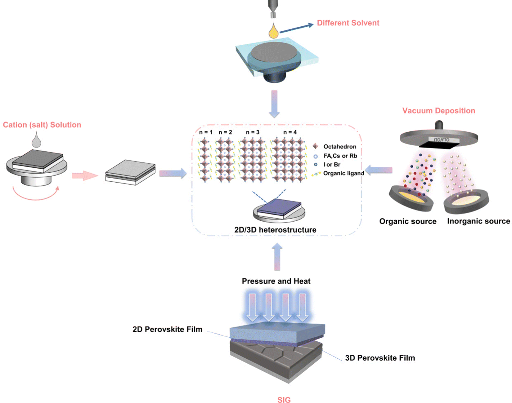 | ||
| Fig. 1 Schematic diagram of the preparation process of the 2D/3D heterostructure precisely controlled phase, including organic cationic ligand, solvent type, vacuum deposition and solid growth under pressure/heat. | ||
5.1 Organic cation engineering
The two-dimensional layer of the 2D/3D heterojunction is usually fabricated by dissolving ammonium salt in a solvent and then depositing it on the surface of three-dimensional perovskite film to form a two-dimensional perovskite layer. Therefore, the most critical element is the large amine cation at the A′ position of 2D perovskite. Fig. 2 shows the chemical structure of the large amine cation commonly used for passivation.77 The concept of 2D/3D superposition was not proposed until 2018, and large amine ions were previously used as three-dimensional defect passivators. The structure and physical properties of solution-treated quantum wells can be adjusted by chemical composition, such as the n value of the thickness of the perovskite layer. Organic cationic ligands affect the energy band structure between the two-dimensional and three-dimensional interfaces by affecting the thickness of the two-dimensional perovskite layer. In the 2D/3D heterojunction structure, a higher dimension n (>5) has not been recorded. The surface energy will change on the basis of surface modification.78,79 With the addition of the surface ligand, the dipole moment of the surface ligand and the direction and size of the bond dipole with the underlying material will lead to changes in the work function. Park et al.80 reported that the MAPbI3 membrane is exposed to the surface ligand solution for a short time, many surface ligands will penetrate MAPbI3, which may have a great impact on PV performance. Dimensional changes caused by energy changes after surface ligand treatment are one of the main reasons for PV performance differences between different ligands. The dimensional changes of 2D in the heterojunction structure affect the ionization energy (IE) and electron affinity energy (EA) of the three-dimensional perovskite, where IE and EA are equivalent to the maximum valence band and the minimum conduction band, respectively. The application of organic cations will have a significant impact on the dimensions (n) of two-dimensional and three-dimensional interfaces in heterojunction structures, and thus influence the band structure between the interfaces.81–85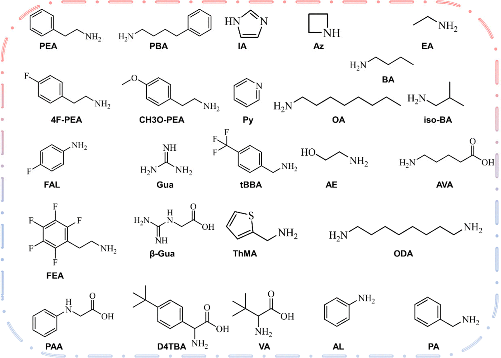 | ||
| Fig. 2 Structures, names and formulas for several types of aliphatic and aromatic amines recently reported in the 2D hybrid organic–inorganic perovskite solar cells. | ||
Lin et al.86 first revealed the 2D/3D heterojunction structure, using three-dimensional perovskite to react with n-butylamine (BA) and n-butylamine iodide (BAI) to form a two-dimensional/three-dimensional superimposed structure, as shown in Fig. 3(a). After BA treatment, the XRD result of two-dimensional perovskite (BA)2PbI4 showed that the dimension (n) was 1. For BAI-treated films, n values of 1–4 were observed, indicating the formation of two-dimensional perovskite mixtures with different n values (Fig. 3(b)). The two-dimensional perovskite layer obtained with two spacer molecules BA and BAI has different components. Due to the different chemical reaction mechanisms, the composition of the resulting two-dimensional perovskites is also different. The iodine ions in BAI react with MAPbI3 to generate MAI, resulting in the generated two-dimensional perovskite n value cannot be fixed, and BA directly reacts with MAPbI3 to generate pure phase two-dimensional perovskite. The higher the BA and BAI concentration, the lower the efficiency of the device. This is because the formed two-dimensional perovskite is too thick and the charge transport performance is poor. The heterojunction structure has better thermal stability than traditional three-dimensional perovskite solar cells. The decrease in defect density inhibits ion migration at both the surface and the grain boundary. The work of Lin and colleagues provides deep insights into the chemical reaction mechanism that forms the 2D/3D stacked structure. Different post-processing is used to adjust the two-dimensional/three-dimensional stacked structure, while improving the performance and stability of perovskite solar cells. Niu and colleagues62 studied the effects of 2D perovskites based on diammonium spacer organic cationic ligands on the structure of 2D quantum wells (QW) and the electronic properties of 2D/3D interfaces. The chemical structure and concentration of the 2D layer spacer layer have a significant impact on the properties of the two-dimensional cover layer, including phase purity and orientation. In the 1,6-diaminohexane ammonia (HDA)-based two-dimensional perovskite film, the formation of the intermediate phase affects the crystallization process of the two-dimensional cover layer, resulting in a wide distribution of QW phases on the three-dimensional perovskite film (n = 1 and n = 2 coexist), and the crystal orientation is uneven as illustrated in Fig. 3(c). The strong molecular interaction between the 2,2-(ethyl enedioxy) bis(ethyl ammonium) (EDBE) cation and the inorganic [PbI6]4− plate promotes the controlled deposition of the horizontally oriented phase pure QW structure (n = 1), which leads to better surface passivation and carrier extraction. The increase of QW disorder in the two-dimensional capping layer will increase the barrier of charge transport in the vertical direction, reducing the charge collection efficiency and corresponding device parameters. A stronger interaction between the EDBE spacer and the perovskite layer results in an enhanced electron density at the edge of the valence band and a reduced energy difference between the perovskite and HTL boundary levels (Fig. 3(d)).
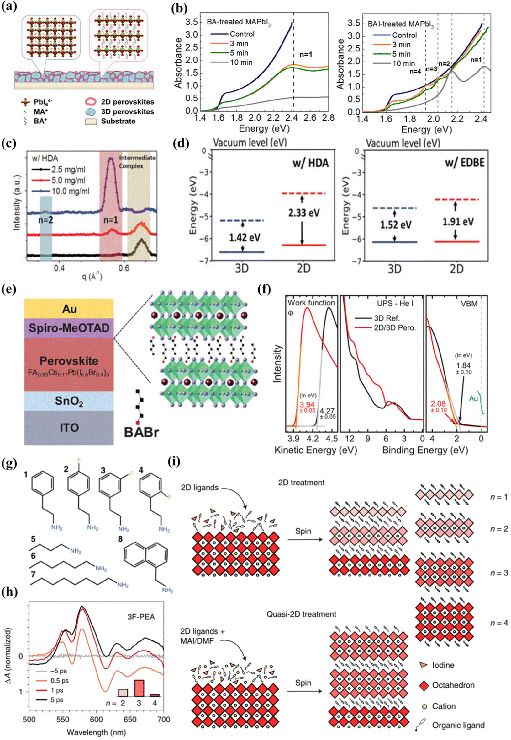 | ||
| Fig. 3 (a) Schematic of the perovskite film treated by BA to form a 2D/3D stacking structure. (b) Absorption spectra of BA-treated MAPbI3 films and BAI-treated MAPbI3 films with different reaction times. Reproduced with permission.86 Copyright 2018 American Chemical Society. (c) Corresponding line-cut profiles from GIWAXS patterns of 2D/3D films along the in-plane directions. (d) Energy-level alignments between the 2D and 3D components (in the model I- and EDBE-based 2D/3D heterostructures, as calculated at the DFT/HSE-SOC level). Reproduced with permission.62 Copyright 2022, Wiley-VCI(e) Schematic of the solar cell based on wide-bandgap Cs0.17FA0.83Pb(I0.6Br0.4)3 perovskite thin-film absorber layers with a 2D-RP interlayer processed by depositing BABr solution on top of the perovskite. (f) UPS measurements of the secondary electron cutoff, the valence band, and the VBM region of the 3D perovskite and the 2D/3D perovskite. Reproduced with permission.57 Copyright 2019, Wiley-VCH. (g) The eight ligands used in the study. (h) TA spectra of films treated with 3F-PEA using the quasi-2D treatment. (i) Schematics of the standard 2D treatment and the quasi-2D treatment producing n ≤ 2 RDPs and n ≥ 2 RDPs, respectively. Reproduced with permission.51 Copyright 2022, Nature Publishing Group. | ||
Gharibzadeh et al.57 spin-coated n-butyl ammonium bromide (BABr) on a three-dimensional perovskite layer, forming a 2D perovskite intermediate layer (n = 2) between the absorber layer and the hole transport layer (HTL), forming a thin 2D/3D perovskite heterostructure (Fig. 3(e)). When the optimal concentration is 2 mg mL−1, the relative control of FF and JSC increases slightly. When the concentration is higher, FF and JSC decrease significantly, due to the low conductivity of the 2D perovskite interface layer, and as the BABr concentration increases, the thickness of the 2D perovskite increases. The disordered 2D-RP perovskite layer has limited electrical conductivity, and only a very thin layer can passivate the 2D/3D perovskite heterostructure. When the BABr concentration is optimal, the work function drops from 4.27 eV (control) to 3.94 eV (target), and the different valence band/orbital structures of the two-dimensional/three-dimensional perovskite heterostructure change significantly in spectral shape over the entire energy range. Compared with the 3D perovskite reference, the VBM of the 2D/3D perovskite heterostructure decreased by 0.24 eV (Fig. 3(f)). The band alignment of wide bandgap perovskite solar cells has been improved by adding BABr to prepare two-dimensional pure phase QWs. The research of Gharibzadeh and colleagues also proves that in 2D/3D heterojunctions, precise control of the 2D perovskite phase is more advantageous than uneven phase distribution. Niu et al.60 reported that in 2D/3D films, regardless of fluorination or composition engineering, template growth of quantum wells is a common characteristic. In a highly parallel-oriented 2D/3D film, the diffraction arc of the quantum well has no periodic characteristics, which indicates that QWs has the characteristics of being induced to grow using a three-dimensional template. The 2D/3D film of the aliphatic spacer n-butyl ammonium- (BA-) and 4,4,4-trifluorobutyl ammonium- (FBA-) group showed phase purity (n = 2) QWs. The films of the aromatic spacers phenylethyl ammonium- (PEA-) and 4-fluorophenyle-thyl ammonium- (FPEA-) groups showed phase impurities (n = 1 and n = 2 coexist) QWs. Compared with fluorinated films, the presence of anisotropic rings in 2D/3D films based on PEA and BA is significantly reduced, which means that the randomness of the quantum well is higher when the spacer is fluorinated. Compared with fluorinated films, the presence of anisotropic rings in 2D/3D films based on PEA and BA is significantly reduced, which means that the randomness of the quantum well is higher when the spacer is fluorinated. For the non-fluorinated spacer layer, QWs obtained a better out-of-plane orientation.
Sam et al.87 proposed to use a very dilute 2D ligand solution (1 mM) and extend the exposure time, which can affect the quantum well distribution without increasing the harmful thickness of the 2D layer. The research results obtained a film with a mainly n = 1 structure. With the extension of the soaking time, the n = 2 diffraction increases with the increase of the soaking time. The perovskite lattice components are highly unstable. Cation exchange and insertion reactions can occur at room temperature, including the complete conversion of pure PbI2 to n = 1 or n = 2 by exposure to the ligand solution, so that the soaking time of the precursor body fluid has an impact on the dimension. Zhang et al.72 reported that a MAPbI3–(BA)2(MA)n−1PbnI3n+1 three-dimensional–two-dimensional perovskite planar heterojunction was realized through a simple ion exchange process between the BAI and MAPbI3 interface. 3D MAPbI3 is pre-deposited during the spin coating process, and the solvent concentration is controlled by dropping a high concentration of BAI tert-butanol solution (20–100 mg mL−1, the solvent is isopropanol) to adjust the layer width distribution. The exciton absorption peaks of 2D perovskite species can be observed at 570 (n = 2), 605 (n = 3) and 645 nm (n = 4) in the UV-visible spectrum when the concentration of tert-butanol solution is 20–100 mg mL−1, and the n value is relatively simple when the concentration is 40 mg mL−1. The maximum valence band values of 3D and 2D perovskites treated with 40 mg mL−1 BAI are −5.5 eV and −5.4 eV. A small VBM difference (0.1 eV) allows hole extraction, while the difference in the CBM between the two-dimensional and three-dimensional layers effectively prevents electron transfer. The optimal band alignment between the 3D perovskite layer and the 2D perovskite passivation layer is achieved by adjusting the BAI solution concentration. Proppe et al.88 reported that combining 2D and 3D perovskites in heterostructures has been shown to take advantage of the high efficiency of most 3D active layers and combine it with the improved stability of the thin 2D top layer. The researchers used the ligand 4-vinylbenzylammonium to form a perovskite quantum well (PQW) on a 3D perovskite layer. It has a highly similar structure to phenethyl ammonium, and the para position of the aromatic benzene ring has an additional terminal vinyl. This extended conjugation helps absorb ultraviolet light (∼250 nm), allowing direct photoexcitation to trigger photochemical crosslinking.89 After the vinyl in the ligand is activated by ultraviolet light, a new covalent bond is formed between the PQW. Orderly n = 1 and n = 2 PQW are formed on top of the 3D active layer in the 2D/3D heterostructure. The heterojunction top layer is exposed to UV light to activate the vinyl in the ligand to form new covalent bonds between the 2D layers. The researchers used ultraviolet photoelectronic spectroscopy (UPS) to estimate the valence band edges of 3D and 2D/3D films, and found that the edge of the 2D perovskite band increased by about 0.3 eV relative to the 3D perovskite. Chen et al.51 reported that in bulk halide perovskite films, the average layer thickness is adjusted by changing the ratio of 2D ligands to 3D perovskite precursors in the solution. Quasi-2D perovskite films made of fluorinated and non-fluorinated PEA ligands will form different QW structures. The researchers tested the PEA-based ligand with fluorine in Fig. 3(g) and found that it had a significant impact on the QW distribution. 3-Fluoro-phenethylammonium (3F-PEA) produces most 2D/3D heterojunctions with n = 3 (Fig. 3h). As shown in Fig. 3(i), this strategy can increase the layer width of the two-dimensional perovskite in the two-dimensional/three-dimensional heterostructure, and can generate n ≥ 3 two-dimensional perovskite overlays. This study also found that π–π stacked ligands form a wider two-dimensional perovskite cover layer due to the slower crystallization rate, which inhibits the formation of a narrower two-dimensional passivation layer.76 This is confirmed by films treated with hexamine (HA) and octamine (OTA) ligands, which indicate that the presence of n ≥ 3 RDP increases with the increase of ligand length. Phenethyl ammonium (PEA) forms a 2D cover layer with dimensions (n) of 2 and 3, while 3F-PEA forms dimensions (n) of 3. Compared with PEA, the specific orientation and arrangement of ligands caused by fluorine atoms in 3F-PEA introduces greater strain, which manifests as greater distortion, so larger perovskite flakes are required to completely release the additional strain. Therefore, the optimal point of n = 3 is formed in the formation energy of 3F-PEA. The 2D passivation layer with a covering layer of n ≥ 3 will be beneficial to the performance of p–i–n solar cells by reducing the carrier transmission resistance. Compared with standard 2D processing equipment, the performance improvement of quasi-2D (n > 1) processing equipment mainly comes from FF and JSC improvements.
From a thermodynamic basis, the difficulty of growing phase pure high-n-element compounds is increased. Calorimetry measurements show that high-n-value compounds have an unfavorable enthalpy of generation (ΔHf). The pure high-n-value RP phase is thermodynamically unstable. As n increases, the Gibbs free energy (ΔG) stabilizes sharply, which limits the possibility of product formation. Therefore, systems that can explain larger n values may not be synthesized in pure phase form.75,90 It is not difficult to understand why in 2D/3D heterojunctions, the high n-value 2D phase usually exists in the form of mixed phase. The n-value of the thickness of the two-dimensional perovskite layer in the heterojunction often also affects the work function and energy band structure between the two-dimensional and three-dimensional interfaces.76,91–93 When a heterojunction is applied to device equipment, the transfer of energy from the CBM is greater than the transfer from the VBM. This increase in CBM will introduce an energy barrier for electron transfer to the ETL. Therefore, although the increase in VBM is expected to have a positive impact on the hole extraction and hole blocking properties of the HTL and ETL interfaces, respectively, the corresponding increase in CBM energy should have a negative impact on the electron extraction of the ETL interface. Changing the width (n) of the two-dimensional passivation layer film will change the energy distribution of the resulting material. When 2D/3D heterojunction structures are used in trans devices, it can also be found that the CBM mismatch between the interfaces leads to large electron blocking, which affects the photovoltaic parameters.
5.2 Solvent engineering
Solution spin coating is the most common method to structure the 2D/3D perovskite heterojunction in which two-dimensional perovskites could be used as the passivation layer. Usually, the precursor solution of ammonium salt or amine molecule is directly spin-coated on the three-dimensional perovskite film, and the two-dimensional passivation layer is obtained by in situ growth. Achieving solution treatment of heterogeneous structures is a long-term challenge for halide perovskites because solvent incompatibility can destroy the underlying layer and result in the formation of mixed phases. Therefore, it is necessary to summarize in detail the types of two-dimensional perovskite passivation layer solvents that have been reported.Most of the organic cations that form 2D perovskites use isopropyl alcohol (IPA) as their precursor solvent. Due to its polarity and ability to form hydrogen bonds, IPA can effectively dissolve organic cations such as MA+ or FA+ on the surface of three-dimensional perovskite.94 This results in mixing (different n values) of two-dimensional passivating layers on 2D/3D heterojunction surfaces. Due to the small gap in formation energy between different layer structures, when the surface is treated with halogen ammonium salt, the number of layers of perovskite will be uncontrollable, so there will be a variety of low-dimensional perovskites with different layers in the film. After the solution is post-treated, dimension-reducing perovskites with n = 1/2 are almost universally formed in 2D/3D structures.63,86,88,95,96
It is well known that the various properties of the solvent, such as the dielectric constant and the solubility of the precursor, will affect the reactivity of the material. In the deposition process of the two-dimensional perovskite passivation layer, improper use of its precursor solution will have an adverse effect on the underlying three-dimensional perovskite, so that a two-dimensional/three-dimensional heterostructure cannot give full play to its maximum advantages. IPA is a common solvent for surface passivation of perovskite films.26,97 However, conventional deposition methods using protic polar solvents (mainly IPA) can lead to instability of the underlying perovskite layer and adverse degradation of device properties. The properties of two-dimensional perovskite synthesized in situ are very important to the selection of solvent. Currently, IPA is not suitable for all materials.94,98,99 Researchers need to make specific analyses for different materials to choose the most suitable solvent.
Jason et al.100 experimentally proved that the commonly used isopropanol has a negative effect on the treatment of the upper layer of three-dimensional perovskite, and reported a selective precursor dissolution strategy using linear alkyl ammonium bromide and chloroform (CF) as the precursor solvent and solute of the 2D perovskite cover layer. As shown in Fig. 4(a), IPA can effectively dissolve formamidine iodide due to its high polarity and ability to form hydrogen bonds, while CF has very limited solubility in FAI. The solubility of n-hexyl ammonium bromide (C6Br) used for in situ synthesis of the two-dimensional passivation layer in the two solvents shows the opposite trend, of which the solubility of C6Br in CF is higher than that of IPA. Through performance and other related tests, it can be proved that the experiment transfers the high-quality two-dimensional cover layer to the three-dimensional perovskite without negatively affecting the underlying three-dimensional perovskite layer (Fig. 4(b and c)). This literature lays the foundation for subsequent research on the solvent selection of two-dimensional perovskite as the passivation layer, so as to avoid the destruction of the solvent on three-dimensional perovskite and the formation of an inferior phase. Randi et al.52 applied ammonium iodide oleate (OLAI) molecules to form a Ruddlesden Popper phase 2D perovskite layer with chloroform as the solvent. The surface defects of 3D perovskite are post-treated, and the dimension n of 2D perovskite fragments is adjusted by adjusting the annealing conditions from a lower temperature to a higher temperature. Because the higher n layer has a lower formation energy. Therefore, the dimension n = 1 of the D perovskite passivation layers prepared by thermal annealing (TA).101 However, after post-treatment with OLAI molecules at room temperature (RT), the high-dimensional 2D perovskite layer dominates (n ≥ 2), as shown in Fig. 4(d and e). The energy difference between EF and VBM of the samples prepared at room temperature was wider, indicating that the N-type characteristics of 3D perovskite films after treatment were enhanced. The valence band value of the target is closer to the CBM of the electron transport layer (C60) at the n-type contact, allowing more efficient charge transfer between the perovskite and the C60 electron selection layer. The energy distribution of RDP can be adjusted by adjusting its layer width (n).
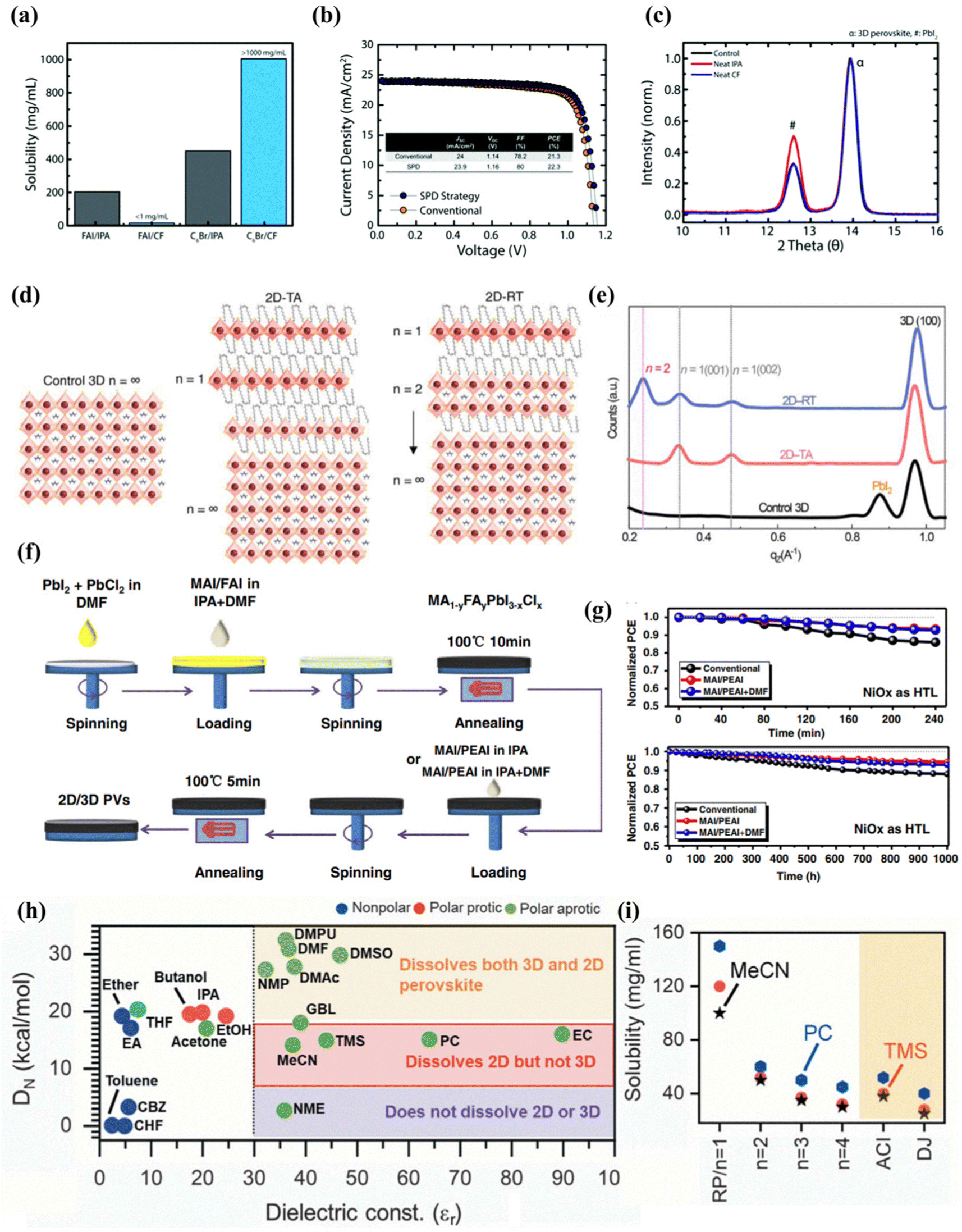 | ||
| Fig. 4 (a) Solubility of FAI and C6Br in CF and IPA illustrating the appropriateness of using CF for the LP treatment. (b) J–V curve of 3D/LP (conventional) and 3D/LP (SPD strategy) PSCs. (c) Grazing incident XRD (GIXRD) of 3D perovskite treated without any solvent (control), with neat IPA, or with neat CF. ‘a’ corresponds to the 3D perovskite diffraction peak and ‘#’ corresponds to the PbI2 diffraction peak. Reproduced with permission.100 Copyright 2019, Royal Society of Chemistry. (d) Schematic illustration of 2D perovskite passivation with different n layers under thermal annealing at 100 °C and a room-temperature process. (e) Integrated intensity of GIWAXS data along qz. Reproduced with permission.52 Copyright 2022, American Association for the Advancement of Science. (f) Schematic procedure for the preparation of mixed 2D/3D perovskite thin films by a three-step spin-coating method. (g) Illumination stability of devices under constant AM 1.5G light, without excluding ultraviolet light and moisture stability of devices under ambient air with RH% 50% for 1000 h without excluding room light. Reproduced with permission.102 Copyright 2019, Wiley-VCH. (h) Plot showing different solvents based on the dielectric constant (εr) and the Gutmann number (DN) to identify the differences in the solubility of the 3D and 2D perovskite powders for making a 3D/2D bilayer stack. (i) Solubility of RP BA2MAn−1PbnI3n+1 (n = 1 to 4), DJ, (4AMP) MAPb2I7, and ACI, (GA)MA2Pb2I7-based 2D perovskites in the solvents MeCN, TMS, and PC as shown. Reproduced with permission.53 Copyright 2022, American Association for the Advancement of Science. | ||
In addition, adding a small amount of N,N-dimethylformamide (DMF) to the traditional solvent isopropanol has also been shown to be effective in constructing 2D/3D heterojunction structures. This may be because the two solvents in the solvent mixture can dissolve different parts of the molecule, so that the solubility of the mixed solvent is better than that of any single solvent, thereby avoiding the formation of inferior phases.
Zhou et al.102 reported a new strategy for dissolving 2-phenylethanamine iodide (PEAI) and DMF in isopropanol as additives to improve the efficiency and stability of two-dimensional/three-dimensional perovskite films. A schematic diagram of this is shown in Fig. 4(f). Adding DMF as a polar solvent to the MAI/PEAI solution, DMF can dissolve the top of the three-dimensional perovskite, which can promote PEAI to penetrate the perovskite to form the best 2D/3D perovskite heterostructure, which is conducive to passivation of the trap state and enhanced charge transport. MAI to reduce the ratio of 2D ligand ions to a-position cations. The research results show that the PCE of the equipment prepared by the new strategy exceeds 22%, and the filling factor (FF) is as high as 83.6%. In the absence of any packaging, after the device is exposed to air for 1000 h, the PCE is still as high as 91% (Fig. 4(g)).
As mentioned earlier, the suitable solvents for different two-dimensional cover layer materials should be specifically analyzed according to the properties of the materials. There are many organic cations for constructing low-dimensional perovskites in 2D/3D heterojunctions, and it is difficult to formulate a standard to measure the suitability of the solvent. However, for the method of directly synthesizing high purity 2D perovskite powder, dissolving it in solvent and then spin coating to construct a 2D/3D heterojunction, without using organic cations to consume excess PbI2 to form 2D perovskites, a suitable solvent becomes relatively easy to screen.
Although the dielectric constant and the Gutman donor number are two different properties, they are related to each other. The dielectric constant refers to the ability of a substance to maintain an electric charge, and for a solvent, it refers to its ability to solvate solute molecules and separate ions. Generally speaking, solvents with a large dielectric constant have a greater ability to separate ions, and they also have a strong solvation ability. In short, it determines the ability of the solvent to dissolve any ionic compound by screening the Coulomb attraction between ions.103,104 The Gutmann donor number essentially measures the alkalinity of the Lewis base of the solvent molecule, and measures the degree to which coordination compounds are formed between the solvent and the cation (high donor number) or between the precursor itself (low donor number). Solvents with high Gutmann numbers will strongly coordinate with divalent metals, thereby inhibiting the formation of molecular clusters.
Siraj et al.53 recently reported in detail the selection requirements of low-dimensional perovskites in two-dimensional/three-dimensional heterojunction. The solvent selection of the two-dimensional cover layer takes advantage of the two basic characteristics of the treated solvent, namely the dielectric constant (εr) and the Gutman donor number (DN), which controls the coordination between the precursor ions and the solvent. A solvent that satisfies both the dielectric constant >30 and the Gutman donor number, 5 < DN < 18 kcal mol−1, can effectively dissolve the 2D perovskite powder during processing such as spin coating, scraping coating or groove mold coating, and will not dissolve or degrade the underlying 3D perovskite film (Fig. 4(h)). According to the two basic characteristics of the selection of four solvents, respectively acetonitrile (MeCN), tetramethyl sulfone (TMS), propylene carbonate (PC), and ethylene carbonate (EC), which can dissolve 2D halide perovskite powder well without causing damage to the lower three-dimensional perovskite (Fig. 4(i)).
After more than ten years of perovskite photovoltaic research, spin coating and general solution treatment are still the most extensive methods for manufacturing PSCs. However, spin coating is very wasteful, the solvent has corrosion problems and is toxic and harmful to the environment and human body, and is not suitable for upgrading commercial applications. This means that other methods must be developed to achieve industrial-scale manufacturing of perovskite photovoltaic devices.
5.3 Mechanical pressing method
Mechanical pressing is expected to contribute to the combination of 2D and 3D perovskites. The SIG process provides a highly crystallized 2D (BA)2PbI4 layer with controllable thickness deposition on top of the 3D film without any quasi-2D phase (n > 1). Jang et al.73 reported a strategy for growth in the solvent-free solid phase plane, growing a highly crystallized 2D (C4H9NH3)2PbI4 film on a 3D perovskite, which may make the constructed heterojunction structure highly complete. They used a SIG process to grow the two-dimensional cover layer by applying pressure and heat to ensure the complete characteristics of the interface contact between the two layers in the entire device. The SIG process avoids the formation of inferior phases to a certain extent.5.4 Vacuum deposition method
Vacuum deposition is another solvent-free technology suitable for assembling multilayer films by using integrated 2D perovskites.105 The vacuum processing of perovskite eliminates problems such as the solubility limit of the deposited 2D perovskite precursor solution or the need for orthogonal solvents to process multilayer devices.106,107 It can well control the thickness of the film and the deposition of a high-purity semiconductor.108,109 Lin et al.110 reported that through the surface evaporation molecular exchange between BAI and MAPbI3 films, a full steam preparation of 3D–2D planar perovskite heterojunction for solar cells was provided. First, the 150 nm PbI2 film is evaporated on the FTO/TiO2 substrate, and then exposed to the MAI vapor environment at 180 °C for 30 min. Finally, the formation of the 2D cover layer is completed by exposing the prepared MAPbI3 film to the BAI vapor (Fig. 5(a)). The transformation of the available form of SEM proceeds over time, and a surface with a smaller layer structure is observed after 60 min of reaction Fig. 5(b–d). X-Ray diffraction is obtained after BAI steam treatment, the diffraction peak does not change until the processing time is increased to 20 min, corresponding to the two-dimensional perovskite diffraction peaks of n = 1 and n = 2 (Fig. 5(e)). UV-Vis spectra also confirmed the presence of 2D (n = 1–3) perovskites in 3D MAPbI3 perovskites (Fig. 5(f)). Studies have shown that large alkylammonium BA has been inserted into the 3D-MAPbI3 structure, and the distance between the inorganic [PbI6] layers is expanded by replacing MA to form a 2D perovskite in the film. Experiments have confirmed that vacuum deposition can regulate the n-value distribution of two-dimensional perovskites in a heterojunction through stem treatment time. As the time exposed to steam increases, the VBM of the device becomes deeper. This means that the holes flowing to the Au back contact will encounter an increasing barrier. This VBM offset will cause holes to accumulate at the interface, resulting in a decrease in JSC (Fig. 5(g)). La-Placa et al.111 reported 2D/3D/2D perovskite heterostructures prepared by a dual-source vacuum deposition process, as shown in Fig. 5(h). The interaction between the 3D and 2D phases and the charge transport characteristics of the 2D passivation layer in the complete 2D/3D interface are investigated. It allows fine control of film thickness and deposition of high-purity semiconductor. The 2D/MAPbI3/2D perovskite heterostructure was prepared by using pure MAPbI3 (3D) and pure phenethyl ammonium iodide (PEA2PbI4, 2D). Unlike the case where 2D is formed after precursor body fluid treatment, vacuum deposition has observed that although there is a large open circuit voltage, the charge transmission is reduced and the evidence for surface passivation is insufficient. No transfer of charge and energy from the two-dimensional film to the 3D film was observed in the MAPI active layer. This may be due to the irreversible orientation of the 2D perovskite passivation layer relative to lead methylammonium iodide (growth parallel to the substrate and hinders charge transmission) and the low dimension of the formation of the 2D passivation layer (n is generally 1). Using 2D perovskite as the passivation layer in p–i–n devices, the decrease in PCE is mainly due to the decrease in current and filling factor.112 The ionization energy (IE) shown in Fig. 5(i) can be used to estimate the maximum value of the valence band (VBM) in the intrinsic semiconductor. The IE of MAPI is 5.0 eV, while the IE of PEA2PbI4 film is 5.5 eV. This means that there is a hole extraction energy barrier of about 0.5 eV, which supports the serious decline in FF observed when PEA2PbI4 is deposited between HTL and MAPI, as illustrated in Fig. 5(j).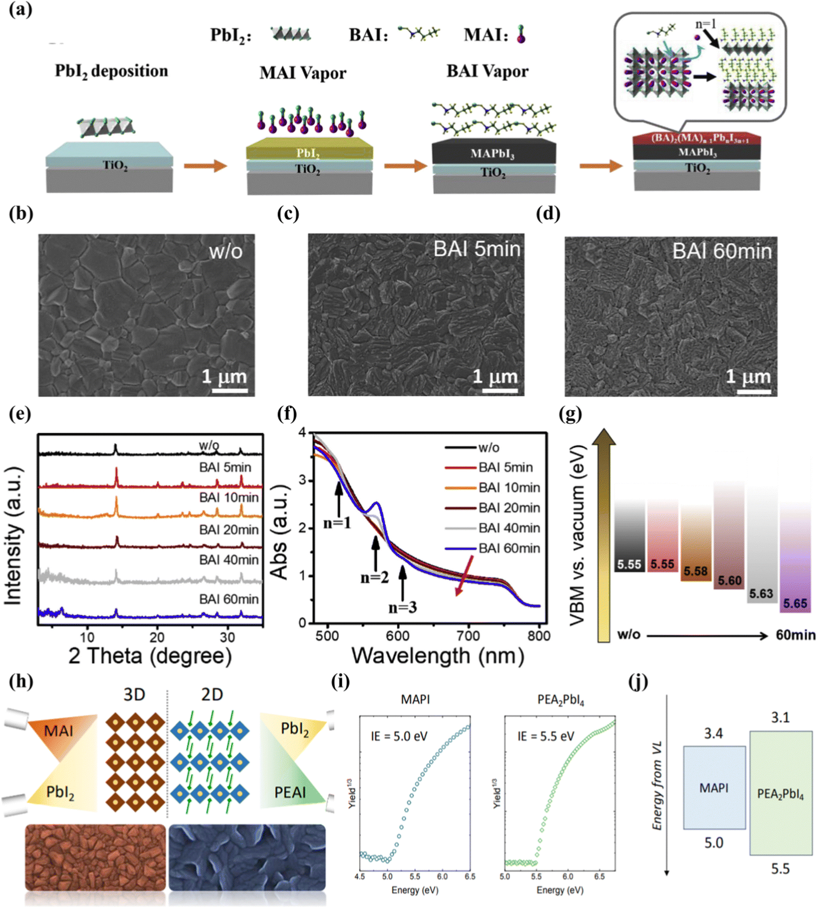 | ||
| Fig. 5 (a) Schematic diagram of the growth of MAPbI3–(BA)2(MA)n−1PbnI3n+1 hybrid structures. The n value describes the perovskite layer numbers between two layers of BA molecules. (b–d) SEM images of the perovskite thin films without (b) and with 5 min (c) and 60 min (d) BAI vapor treatment. (e) XRD patterns and (f) UV-Vis spectra of perovskite films with different times for BAI vapor treatment. (g) Calculated VBM. As the charging effect cannot be fully excluded from the current data, absolute values cannot be taken seriously. Reproduced with permission.110 Copyright 2019, Elsevier Ltd. (h) Schematic diagram of the vacuum deposition 2D/3D perovskite heterojunction strategy. (i) Air Photoelectron spectroscopy (APS) for vacuum deposited MAPI and PEA2PbI4 thin films. (j) Flat band energy diagram with measured ionization energies (IE) and estimated electron affinity taking into account the bandgap of the two materials. Reproduced with permission.111 Copyright 2019, American Chemical Society. | ||
The vacuum deposition method can also be used for large area and high throughput treatment of perovskite. Feng et al.113 prepared large area uniform and high-quality perovskite films on rigid (400 cm2) and flexible (300 cm2) substrates. In addition, a low temperature vacuum annealing process was developed to produce high density formamidine perovskite films. The study found that the performance of perovskite solar cells is seriously affected by the vacuum annealing temperature. When the annealing temperature is optimized to 60 °C, the efficiency of the resulting perovskite solar cell will be increased to 21.32%, which is the highest efficiency of perovskite solar cells manufactured using a vacuum deposition process. Thanks to the solvent-free and air-free environment, perovskite solar cells prepared using a vacuum deposition process exhibit excellent long-term stability.
Both mechanical pressing and vacuum deposition methods can prepare a high-purity phase 2D cover layer for passivation of 3D perovskites to form a complete interface. However, the dimension (n) formed by the two strategies is very low, usually approximately equal to 1, and its preparation process takes several hours, which increases manufacturing costs. In addition, long-term deposition has an adverse effect on the oxide buried layer, which is not conducive to device performance.
6. Summary and outlook
In this review, we summarized the latest progress of 2D/3D heterojunctions in PSCs, including the filter rules of precursors, the mechanisms of defect passivation, the adjusting methods of dimensional (n) distribution and the fabrication process of 2D/3D heterojunctions. In addition, some emerging challenges in the efficient utilization of 2D/3D perovskite heterojunctions in PSCs, such as controlling the regulation of film thickness, and the low current and filling factor caused by electronic blocking in the 2D layer of inverted (p–i–n) devices, have been elaborated and the potential solutions for these challenges have also been discussed in depth.The selection of the precursor solvent of two-dimensional perovskite for a 2D/3D heterojunction has a great influence on the characteristics of carrier transport and energy band arrangement at the crystal surface of the grain boundary. By changing the precursor solvent, the two-dimensional perovskites in the heterojunction can form different n-value distributions. Improper solvent selection will lead to the formation of inferior phases at the heterojunction interface. Therefore, researchers should not only consider whether the solvent dissolves the two-dimensional ligand, but also whether the solvent has an adverse effect on the three-dimensional perovskites. The composition of three-dimensional perovskites is different, and the suitable two-dimensional perovskite ligand solution may also be changed. For constructing heterojunction structures, solution characteristics such as the dielectric constant and Gutman donor number could be considered to screen suitable organic ligand solutions for forming two-dimensional perovskite layers according to different three-dimensional perovskite systems. Hence, the solubility of the solution to organic cations should also be one of the options for screening suitable solvents.
In addition, the 2D perovskite size (n) at the electron transport interface in the pin structure is critical for effective top contact passivation. The uneven distribution of the n value of the 2d perovskite layer in the heterojunction structure will limit the transmission of electrons and holes. When two-dimensional perovskites are formed, different ligands produce different n distributions. The organic matters with larger volume possess a slower embedding speed, which leads to a larger n value, thus making the film thicker with the increase of the layer width. 2D perovskite films prepared by fluorine-containing organic cations may be of greater value in p–i–n devices because they can form different quantum well structures. At present, organic cation engineering and solvent type adjustment only play a role in regulating the n value but cannot accurately control the dimension of the two-dimensional perovskite. Fortunately, the SIG process can regulate the crystal orientation of the 2D phase on 3D perovskite films, and the n-phase distribution can be strictly controlled. Using pre-synthesized pure two-dimensional perovskites with different n values, the target two-dimensional perovskite can be combined on the three-dimensional perovskite without loss through the high temperature and high-pressure process of SIG.
Recently, a study on constructing 2D/3D heterojunction structures through the fabrication of a 2D perovskite layer on the 3D perovskite surface has made remarkable achievements in terms of higher efficiency and better stability. And the 2D/3D heterojunction structure of metal halide perovskites is widely used in various photoelectric devices, including solar cells, photodetectors, light-emitting diodes (LEDs) and lasers. These plentiful application scenarios have confirmed that the 2D/3D heterojunction possesses attractive potential for overcoming the inherent disadvantages of perovskite materials and improving the performance of perovskite devices. For perovskite solar cells, the current device efficiency (PCE) based on the 2D/3D heterojunction structure exceeded 25% with outstanding stability even under long-term continuous illumination.51 Accordingly, we believe that this 2D/3D perovskite layered heterojunction will lay a solid foundation for the commercial application of perovskite solar cells in the foreseeable future.
Conflicts of interest
There are no conflicts to declare.Acknowledgements
This work was financially supported by the National Natural Science Foundation of China (62274018, 61904072 and 52002070), and the Fundamental Research Projects of Yunnan Province, China (202001AU070025 and 202101BE070001-049).References
- J. Chen and N. G. Park, Adv. Mater., 2019, 31, 1803019 CrossRef CAS PubMed.
- A. Mei, X. Li, L. F. Liu, Z. L. Ku, T. F. Liu, Y. G. Rong, M. Xu, M. Hu, J. Z. Chen, Y. Yang, M. Grätzel and H. W. Han, Science, 2014, 345, 295–298 CrossRef CAS PubMed.
- N. G. Park, Mater. Today, 2015, 18, 65–72 CrossRef CAS.
- F. Z. Liu, Q. Dong, M. K. Wong, A. B. Djurišic, A. Ng, Z. W. Ren, Q. Shen, C. Surya, W. K. Chan, J. Wang, A. M. Ng, C. Z. Liao, H. K. Li, K. Shih, C. R. Wei, H. M. Su and J. F. Dai, Adv. Energy Mater., 2016, 6, 1502206 CrossRef.
- R. Meng, G. B. Wu, J. Y. Zhou, H. Q. Zhou, H. H. Fang, M. A. Loi and Y. Zhang, Chem. – Eur. J., 2019, 25, 5480–5488 CrossRef CAS PubMed.
- G. B. Wu, J. Y. Zhou, R. Meng, B. D. Xue, H. Q. Zhou, Z. Y. Tang and Y. Zhang, Phys. Chem. Chem. Phys., 2019, 21, 3106–3113 RSC.
- Q. Zhou, D. M. He, Q. X. Zhuang, B. B. Liu, R. Li, H. X. Li, Z. Y. Zhang, H. Yang, P. J. Zhao, Y. He, Z. G. Zang and J. Z. Chen, Adv. Funct. Mater., 2022, 32, 2205507 CrossRef CAS.
- W. Li, Z. M. Wang, F. Deschler, S. Gao, H. F. Richard and K. C. Anthony, Nat. Rev. Mater., 2017, 2, 1–18 Search PubMed.
- J. S. Huang, Y. B. Yuan, Y. C. Shao and Y. F. Yan, Nat. Rev. Mater., 2017, 2, 1–19 Search PubMed.
- T. M. Brenner, D. A. Egger, L. Kronik, G. Hodes and D. Cahen, Nat. Rev. Mater., 2016, 1, 1–16 Search PubMed.
- M. A. Green, E. D. Dunlop, G. Siefer, M. Yoshita, N. Kopidakis, K. Bothe and X. J. Hao, Prog. Photovolt., 2021, 29, 3–15 CrossRef.
- C. Z. Li, R. L. Zhu, Z. Yang, J. Lai, J. J. Tan, Y. Luo and S. J. Ye, Angew. Chem., Int. Ed., 2022, e202214208 Search PubMed.
- L. X. Zhang, X. Y. Pan, L. Liu and L. M. Ding, J. Semicond., 2022, 43, 030203 CrossRef.
- H. X. Wang, L. X. Zhang, M. Cheng and L. M. Ding, J. Semicond., 2022, 43, 080202 CrossRef.
- Y. H. Cheng and L. M. Ding, Energy Environ. Sci., 2021, 14, 3233–3255 RSC.
- X. X. Ren, L. X. Zhang, Y. B. Yuan and L. M. Ding, J. Semicond., 2021, 42, 010201 CrossRef CAS.
- G. B. Wu, R. Liang, M. Z. Ge, G. X. Sun, Y. Zhang and G. C. Xing, Adv. Mater., 2022, 34, 2105635 CrossRef CAS PubMed.
- M. J. Li, L. X. Zhang, C. Chen, J. Z. Chen and L. M. Ding, J. Semicond., 2023, 44, 010201 CrossRef.
- D. M. He, T. W. Zhou, B. B. Liu, L. Bai, W. Q. Wang, H. K. Yuan, C. Y. Xu, Q. L. Song, D. Lee, Z. G. Zang, L. M. Ding and J. Z. Chen, EcoMat, 2022, 4, e12158 CrossRef CAS.
- D. Y. Gao, L. Q. Yang, X. H. Ma, X. N. Shang, C. Wang, M. J. Li, X. M. Zhuang, B. X. Zhang, H. W. Song, J. Z. Chen and C. Chen, J. Energy Chem., 2022, 69, 659–666 CrossRef CAS.
- B. B. Liu, H. Bi, D. M. He, L. Bai, W. Q. Wang, H. K. Yuan, Q. L. Song, P. Y. Su, Z. G. Zang, T. W. Zhou and J. Z. Chen, ACS Energy Lett., 2021, 6, 2526–2538 CrossRef CAS.
- Q. Z. An, F. Paulus, D. Becker-Koch, C. Cho, Q. Sun, A. Weu, S. Bitton, N. Tessler and Y. Vaynzof, Matter, 2021, 4, 1683–1701 CrossRef CAS.
- T. Leijtens, G. E. Eperon, A. J. Barker, G. Grancini, W. Zhang, J. M. Ball, A. R. S. Kandada, H. J. Snaith and A. Petrozza, Energy Environ. Sci., 2016, 9, 3472–3481 RSC.
- W. E. I. Sha, H. Zhang, Z. S. Wang, H. L. Zhu, X. G. Ren, F. Lin, A. K. Y. Jen and W. C. H. Choy, Adv. Energy Mater., 2018, 8, 1701586 CrossRef.
- S.-H. Turren-Cruz, A. Hagfeldt and M. Saliba, Science, 2018, 362, 449–453 CrossRef CAS PubMed.
- Q. Jiang, Y. Zhao, X. W. Zhang, X. L. Yang, Y. Chen, Z. Chu, Q. F. Ye, X. X. Li, Z. G. Yin and J. B. You, Nat. Photonics, 2019, 13, 460–466 CrossRef CAS.
- M. J. Kim, G.-H. Kim, T. K. Lee, I. W. Choi, H. W. Choi, Y. Jo, Y. J. Yoon, J. W. Kim, J. Lee, D. H. Huh, H. Lee, S. K. Kwak, J. Y. Kim and D. S. Kim, Joule, 2019, 3, 2179–2192 CrossRef CAS.
- H. Min, M. Kim, S.-U. Lee, H. Kim, G. Kim, K. Choi, J. H. Lee and S. Seok, Science, 2019, 366, 749–753 CrossRef CAS PubMed.
- X. P. Zheng, Y. Hou, C. X. Bao, J. Yin, F. L. Yuan, Z. Huang, K. P. Song, J. K. Liu, J. Troughton, N. Gasparini, C. Zhou, Y. B. Lin, D.-J. Xue, B. Chen, A. K. Johnston, N. Wei, M. N. Hedhili, M. Y. Wei, A. Y. Alsalloum, P. Maity, B. Turedi, C. Yang, D. Baran, T. D. Anthopoulos, Y. Han, Z. H. Lu, O. F. Mohammed, F. Gao, E. H. Sargent and O. M. Bakr, Nat. Energy, 2020, 5, 131–140 CrossRef CAS.
- M. Cheng, C. T. Zuo, Y. Z. Wu, Z. G. Li, B. M. Xu, Y. Hua and L. M. Ding, Sci. Bull., 2020, 65, 1237–1241 CrossRef CAS PubMed.
- H. Zhang, X. G. Ren, X. W. Chen, J. Mao, J. Q. Cheng, Y. Zhao, Y. H. Liu, J. Milic, W. J. Yin, M. Grätzel and W. C. H. Choy, Energy Environ. Sci., 2018, 11, 2253–2262 RSC.
- M. Saliba, Adv. Energy Mater., 2019, 9, 1803754 CrossRef.
- E. Aydin, M. D. Bastiani and S. D. Wolf, Adv. Mater., 2019, 31, 1900428 CrossRef PubMed.
- N. X. Li, S. X. Tao, Y. H. Chen, X. X. Niu, C. K. Onwudinanti, C. Hu, Z. W. Qiu, Z. Q. Xu, G. H. J. Zheng, L. G. Wang, Y. Zhang, L. Li, H. F. Liu, Y. Z. Lun, J. W. Hong, X. Y. Wang, Y. Q. Liu, H. P. Xie, Y. L. Gao, Y. Bai, S. H. Yang, G. Brocks, Q. Chen and H. P. Zhou, Nat. Energy, 2019, 4, 408–415 CrossRef CAS.
- M. Abdi-Jalebi, Z. Andaji-Garmaroudi, S. Cacovich, C. Stavrakas, B. Philippe, J. M. Richter, M. Alsari, E. P. Booker, E. M. Hutter, A. J. Pearson, S. Lilliu, T. J. Savenije, H. Rensmo, G. Divitini, C. Ducati, R. H. Friend and S. D. Stranks, Nature, 2018, 555, 497–501 CrossRef CAS PubMed.
- M. Saliba, T. Matsui, K. Domanski, J. Y. Seo, A. Ummadisingu, S. M. Zakeeruddin, J. P. Correa-Baena, W. R. Tress, A. Abate, A. Hagfeldt and M. Grätzel, Science, 2016, 354, 206–209 CrossRef CAS PubMed.
- M. J. Li, H. Y. Li, Q. X. Zhuang, D. M. He, B. B. Liu, C. Chen, B. X. Zhang, T. Pauporté, Z. G. Zang and J. Z. Chen, Angew. Chem., Int. Ed., 2022, 61, e202206914 CAS.
- L. Bai, F. Yao, R. Wang, B. B. Liu, D. M. He, Q. Zhou, W. Q. Wang, C. Y. Xu, X. B. Hu, S. Q. Chen, Q. L. Song, T. W. Zhou, D. Lee, P. J. Zhao, C. Chen, H. Yang, Q. Q. Lin, Z. G. Zang and J. Z. Chen, Sci. China Mater., 2022, 65, 1–14 Search PubMed.
- H. Tan, A. Jain, O. Voznyy, X. Z. Lan, F. P. G. Arquer, J. Z. Fan, R. Quintero-Bermudez, M. J. Yuan, B. Zhang, Y. C. Zhao, F. J. Fan, P. C. Li, L. N. Quan, Y. B. Zhao, Z. H. Lu, Z. Y. Yang, S. Hoogland and E. H. Sargent, Science, 2017, 355, 722–726 CrossRef CAS PubMed.
- X. Q. Shi, Y. Ding, S. J. Zhou, B. Zhang, M. L. Cai, J. X. Yao, L. H. Hu, J. H. Wu, S. Y. Dai and M. K. Nazeeruddin, Adv. Sci., 2019, 6, 1901213 CrossRef CAS PubMed.
- D. Yang, R. X. Yang, K. Wang, C. C. Wu, X. J. Zhu, J. S. Feng, X. D. Ren, G. J. Fang, S. Priya and S. Z. Liu, Nat. Commun., 2018, 9, 1–11 CrossRef PubMed.
- W. Hui, Y. G. Yang, Q. Xu, H. Gu, S. L. Feng, Z. H. Su, M. Zhang, J. Wang, X. D. Li, J. F. Fang, F. Xia, Y. D. Xia, Y. H. Chen, X. Y. Gao and W. Huang, Adv. Mater., 2020, 32, 1906374 CrossRef CAS PubMed.
- T. L. Bu, J. Li, F. Zheng, W. J. Chen, X. M. Wen, Z. L. Ku, Y. Peng, J. Zhong, Y. B. Cheng and F. Z. Huang, Nat. Commun., 2018, 9, 1–10 CrossRef CAS PubMed.
- W. Chen, L. M. Xu, X. Y. Feng, J. S. Jie and Z. B. He, Adv. Mater., 2017, 29, 1603923 CrossRef PubMed.
- K. A. Bush, C. D. Bailie, Y. Chen, A. R. Bowring, W. Wang, W. Ma, T. Leijtens, F. Moghadam and M. D. McGehee, Adv. Mater., 2016, 28, 3937–3943 CrossRef CAS PubMed.
- X. Zuo, B. Kim, B. B. Liu, D. M. He, L. Bai, W. Q. Wang, C. Y. Xu, Q. L. Song, C. Y. Jia, Z. G. Zang, D. Lee, X. Li and J. Z. Chen, Chem. Eng. J., 2022, 431, 133209 CrossRef CAS.
- C. Zhang, H. X. Wang, H. Y. Li, Q. X. Zhuang, C. Gong, X. F. Hu, W. S. Cai, S. Y. Zhao, J. Z. Chen and Z. G. Zang, J. Energy Chem., 2021, 63, 452–460 CrossRef CAS.
- H. Bi, B. B. Liu, D. M. He, L. Bai, W. Q. Wang, Z. G. Zang and J. Z. Chen, Chem. Eng. J., 2021, 418, 129375 CrossRef CAS.
- Q. X. Zhuang, C. Zhang, C. Gong, H. Y. Li, H. X. Li, Z. Y. Zhang, H. Yang, J. Z. Chen and Z. G. Zang, Nano Energy, 2022, 102, 107747 CrossRef CAS.
- J. L. Yan, W. M. Qiu, G. Wu, P. Heremans and H. Z. Chen, J. Mater. Chem. A, 2018, 6, 11063–11077 RSC.
- H. Chen, S. Teale, B. Chen, Y. H. L. Grater, T. Zhu, K. Bertens, S. M. Park, H. R. Atapattu, Y. J. Gao, M. Y. Wei, A. K. Johnston, Q. L. Zhou, K. M. Xu, D. N. Yu, C. C. Han, T. Cui, E. H. Jung, C. Zhou, W. J. Zhou, A. H. Proppe, S. Hoogland, F. Laquai, T. Filleter, K. R. Graham, Z. J. Ning and E. H. Sargent, Nat. Photonics, 2022, 16, 352–358 CrossRef CAS.
- R. Azmi, E. Ugur, A. Seitkhan, F. Aljamaan, A. S. Subbiah, J. Liu, G. T. Harrison, M. I. Nugraha, M. K. Eswaran, M. Babics, Y. Chen, F. Z. Xu, T. G. Allen, A. Rehman, C. L. Wang, T. D. Anthopoulos, U. Schwingenschlögl, M. D. Bastiani, E. Aydin and S. D. Wolf, Science, 2022, 376, 73–77 CrossRef CAS PubMed.
- S. Sidhik, Y. F. Wang, M. D. Siena, R. Asadpour, A. J. Torma, T. Terlier, K. Ho, W. B. Li, A. B. Puthirath, X. T. Shuai, A. Agrawal, B. Traore, M. Jones, R. Giridharagopal, P. M. Ajayan, J. Strzalka, D. S. Ginger, C. Katan, M. A. Alam, J. Even, M. G. Kanatzidis and A. D. Mohite, Science, 2022, 377, 1425–1430 CrossRef CAS PubMed.
- B. B. Liu, J. Hu, D. M. He, L. Bai, Q. Zhou, W. Q. Wang, C. Y. Xu, Q. L. Song, D. Lee, P. J. Zhao, F. Hao, X. B. Niu, Z. G. Zang and J. Z. Chen, ACS Appl. Mater. Inter., 2022, 14, 21079–21088 CrossRef CAS PubMed.
- Y. Lin, Y. Bai, Y. J. Fang, Q. Wang, Y. H. Deng and J. S. Huang, ACS Energy Lett., 2017, 2, 1571–1572 CrossRef CAS.
- T. Ye, A. Bruno, G. F. Han, T. M. Koh, J. Li, N. F. Jamaludin, C. Soci, S. G. Mhaisalkar and W. L. Leong, Adv. Funct. Mater., 2018, 28, 1801654 CrossRef.
- S. Gharibzadeh, B. A. Nejand, M. Jakoby, T. Abzieher, D. Hauschild, S. Moghadamzadeh, J. A. Schwenzer, P. Brenner, R. Schmager, A. A. Haghighirad, L. Weinhardt, U. Lemmer, B. S. Richards, I. A. Howard and U. W. Paetzold, Adv. Energy Mater., 2019, 9, 1803699 CrossRef.
- Q. Q. He, M. Worku, L. J. Xu, C. K. Zhou, H. R. Lin, A. J. Robb, K. Hanson, Y. Xin and B. W. Ma, ACS Appl. Mater. Inter., 2019, 12, 1159–1168 CrossRef PubMed.
- L. Iagher and L. Etgar, ACS Energy Lett., 2018, 3, 366–372 CrossRef CAS.
- T. Q. Niu, J. Lu, X. G. Jia, Z. Xu, M. C. Tang, D. Y. Barrit, N. Y. Yuan, J. N. Ding, X. Zhang, Y. Y. Fan, T. Luo, Y. L. Zhang, D. M. Smilgies, Z. K. Liu, A. Amassian, S. Y. Jin, K. Zhao and S. Z. Liu, Nano Lett., 2019, 19, 7181–7190 CrossRef CAS PubMed.
- P. Y. Su, L. Bai, H. Bi, B. B. Liu, D. M. He, W. Q. Wang, X. B. Cao, S. Chen, D. Lee, H. Yang, Z. G. Zang and J. Z. Chen, ACS Appl. Mater. Inter., 2021, 13, 29567–29575 CrossRef CAS PubMed.
- T. Q. Niu, Y. M. Xie, Q. F. Xue, S. N. Xun, Q. Yao, F. C. Zhen, W. B. Yan, H. Li, J. L. Brédas, H. L. Yip and Y. Cao, Adv. Energy Mater., 2022, 12, 2102973 CrossRef CAS.
- D. H. Cao, C. C. Stoumpos, O. K. Farha, J. T. Hupp and M. G. Kanatzidis, J. Am. Chem. Soc., 2015, 137, 7843–7850 CrossRef CAS PubMed.
- J. M. Yang, S. B. Xiong, J. N. Song, H. B. Wu, Y. H. Zeng, L. Y. Lu, K. C. Shen, T. Y. Hao, Z. F. Ma, F. Liu, C. G. Duan, M. Fahlman and Q. Y. Bao, Adv. Energy Mater., 2020, 10, 2000687 CrossRef CAS.
- Y. Bai, S. Xiao, C. Hu, T. Zhang, X. Y. Meng, H. Lin, Y. L. Yang and S. H. Yang, Adv. Energy Mater., 2017, 7, 1701038 CrossRef.
- J. Z. Chen, J. Y. Seo and N. G. Park, Adv. Energy Mater., 2018, 8, 1702714 CrossRef.
- Y. Cai, J. L. Wen, Z. K. Liu, F. Qian, C. Y. Duan, K. He, W. J. Zhao, S. Zhan, S. M. Yang, J. Cui and S. Z. Liu, J. Energy Chem., 2022, 65, 480–489 CrossRef CAS.
- C. Y. Deng, J. H. Wu, Y. T. Du, Q. Chen, Z. Y. Song, G. D. Li, X. B. Wang, J. M. Lin, W. H. Sun, M. L. Huang, Y. F. Huang, P. Gao and Z. Lan, Small Methods, 2021, 5, 2101000 CrossRef CAS PubMed.
- S. Jeong, S. Seo, H. Yang, H. Park, S. Shin, H. Ahn, D. Lee, J. H. Park, N. G. Park and H. Shin, Adv. Energy Mater., 2021, 11, 2102236 CrossRef CAS.
- M. S. He, J. H. Liang, Z. F. Zhang, Y. K. Qiu, Z. H. Deng, H. Xu, J. L. Wang, Y. J. Yang, Z. H. Chen and C. C. Chen, J. Mater. Chem. A, 2020, 8, 25831–25841 RSC.
- Z. He, Y. Zhou, C. Xu, Y. J. Su, A. Liu, Y. Q. Li, L. G. Gao and T. L. Ma, J. Phys. Chem. C, 2021, 125, 16428–16434 CrossRef CAS.
- T. K. Zhang, M. Z. Long, M. C. Qin, X. H. Lu, S. Chen, F. Y. Xie, L. Gong, J. Chen, M. Chu, Q. Miao, Z. F. Chen, W. Y. Xu, P. Y. Liu, W. G. Xie and J. B. Xu, Joule, 2018, 2, 2706–2721 CrossRef CAS.
- Y. W. Jang, S. Lee, K. M. Yeom, K. Jeong, K. Choi, M. Choi and J. H. Noh, Nat. Energy, 2021, 6, 63–71 CrossRef CAS.
- A. H. Proppe, R. Q. Bermudez, H. R. Tan, O. Voznyy, S. O. Kelley and E. H. Sargent, J. Am. Chem. Soc., 2018, 140, 2890–2896 CrossRef CAS PubMed.
- C. O. Cervantes, P. C. Monroy and D. S. Ibarra, ChemSusChem, 2019, 12, 1560–1575 CrossRef PubMed.
- R. Q. Bermudez, A. G. Parker, A. H. Proppe, R. Munir, Z. Y. Yang, S. O. Kelley, A. Amassian, M. F. Toney and E. H. Sargent, Nat. Mater., 2018, 17, 900–907 CrossRef PubMed.
- S. Ahmad and X. Guo, Chin. Chem. Lett., 2018, 29, 657–663 CrossRef CAS.
- B. Boer, A. Hadipour, M. M. Mandoc, T. V. Woudenbergh and P. W. M. Blom, Adv. Mater., 2005, 17, 621–625 CrossRef.
- X. Crispin, Sol. Energy Mater. Sol. Cells, 2004, 83, 147–168 CrossRef CAS.
- S. M. Park, A. Abtahi, A. M. Boehm and K. R. Graham, ACS Energy Lett., 2020, 5, 799–806 CrossRef CAS.
- M. Stolterfoht, P. Caprioglio, C. M. Wolff, J. A. Márquez, J. Nordmann, S. S. Zhang, D. Rothhardt, U. Hörmann, Y. Amir, A. Redinger, L. Kegelmann, F. S. Zu, S. Albrecht, N. Koch, T. Kirchartz, M. Saliba, T. Unold and D. Neher, Energy Environ. Sci., 2019, 12, 2778–2788 RSC.
- P. Schulz, D. Cahen and A. Kahn, Chem. Rev., 2019, 119, 3349–3417 CrossRef CAS PubMed.
- S. M. Park, S. M. Mazza, Z. M. Liang, A. Abtahi, A. M. Boehm, S. R. Parkin, J. E. Anthony and K. R. Graham, ACS Appl. Mater. Inter., 2018, 10, 15548–15557 CrossRef CAS PubMed.
- R. Q. Bermudez, A. H. Proppe, A. Mahata, P. Todorović, S. O. Kelley, F. D. Angelis and E. H. Sargent, J. Am. Chem. Soc., 2019, 141, 13459–13467 CrossRef PubMed.
- J. Emara, T. Schnier, N. Pourdavoud, T. Riedl, K. Meerholz and S. Olthof, Adv. Mater., 2016, 28, 553–559 CrossRef CAS PubMed.
- Y. Lin, Y. Bai, Y. J. Fang, Z. L. Chen, S. Yang, X. P. Zheng, S. Tang, Y. Liu, J. J. Zhao and J. S. Huang, J. Phys. Chem. Lett., 2018, 9, 654–658 CrossRef CAS PubMed.
- S. Teale, A. H. Proppe, E. H. Jung, A. Johnston, D. H. Parmar, B. Chen, Y. Hou, S. O. Kelley and E. H. Sargent, J. Phys. Chem. Lett., 2020, 11, 5115–5119 CrossRef CAS PubMed.
- A. H. Proppe, M. Y. Wei, B. Chen, R. Q. Bermudez, S. O. Kelley and E. H. Sargent, J. Am. Chem. Soc., 2019, 141, 14180–14189 CrossRef CAS PubMed.
- W. Rodebush and I. Feldman, J. Am. Chem. Soc., 1946, 68, 896–899 CrossRef CAS PubMed.
- C. M. M. Soea, G. P. Nagabhushanac, R. Shivaramaiahc, H. Tsaie, W. Y. Nie, J. C. Blancone, F. Melkonyan, D. H. Cao, B. Traoréf, L. Pedesseaug, M. Kepenekianf, C. Katan, J. Even, T. J. Marks, A. Navrotsky, A. D. Mohitee, C. C. Stoumpos and M. G. Kanatzidis, Proc. Natl. Acad. Sci. U. S. A., 2019, 116, 58–66 CrossRef PubMed.
- J. X. Liu, J. Leng, K. F. Wu, J. Zhang and S. Y. Jin, J. Am. Chem. Soc., 2017, 139, 1432–1435 CrossRef CAS PubMed.
- H. H. Tsai, W. Y. Nie, J. C. Blancon, C. C. Stoumpos, R. Asadpour, B. Harutyunyan, A. J. Neukirch, R. Verduzco, J. J. Crochet, S. Tretiak, L. Pedesseau, J. Even, M. A. Alam, G. Gupta, J. Lou, P. M. Ajayan, M. J. Bedzyk, M. G. Kanatzidis and A. D. Mohite, Nature, 2016, 536, 312–316 CrossRef CAS PubMed.
- X. Zhang, R. Munir, Z. Xu, Y. C. Liu, H. Tsai, W. Y. Nie, J. B. Li, T. Q. Niu, D. M. Smilgies, M. G. Kanatzidis, A. D. Mohite, K. Zhao, A. Amassian and S. Z. Liu, Adv. Mater., 2018, 30, 1707166 CrossRef PubMed.
- J. K. Sun, S. Huang, X. Z. Liu, Q. Xu, Q. H. Zhang, W. J. Jiang, D. J. Xue, J. C. Xu, J. Y. Ma, J. Ding, Q. Q. Ge, L. Gu, X. H. Fang, H. Z. Zhong, J. S. Hu and L. J. Wan, J. Am. Chem. Soc., 2018, 140, 11705–11715 CrossRef CAS PubMed.
- A. A. Sutanto, R. Szostak, N. Drigo, V. I. E. Queloz, P. E. Marchezi, J. C. Germino, H. C. N. Tolentino, M. K. Nazeeruddin, A. F. Nogueira and G. Grancini, Nano Lett., 2020, 20, 3992–3998 CrossRef CAS PubMed.
- K. T. Cho, G. Grancini, Y. H. Lee, E. Oveisi, J. Ryu, O. Almora, M. Tschumi, P. A. Schouwink, G. Seo, S. Heo, J. Park, J. Jang, S. Paek, G. G. Belmonte and M. K. Nazeeruddin, Energy Environ. Sci., 2018, 11, 952–959 RSC.
- N. Sun, W. Y. Gao, H. Dong, Y. H. Liu, X. Liu, Z. B. Wu, L. Song, C. X. Ran and Y. H. Chen, ACS Energy Lett., 2021, 6, 2863–2875 CrossRef CAS.
- A. Swarnkar, A. R. Marshall, E. M. Sanehira, B. D. Chernomordik, D. T. Moore, J. A. Christians, T. Chakrabarti and J. M. Luther, Science, 2016, 354, 92–95 CrossRef CAS PubMed.
- K. B. Lin, J. Xing, L. N. Quan, F. P. G. Arquer, X. W. Gong, J. X. Lu, L. Q. Xie, W. J. Zhao, D. Zhang, C. Z. Yan, W. Q. Li, X. Y. Liu, Y. Lu, J. Kirman, E. H. Sargent, Q. H. Xiong and Z. H. Wei, Nature, 2018, 562, 245–248 CrossRef CAS PubMed.
- J. J. Yoo, S. Wieghold, M. C. Sponseller, M. R. Chua, S. N. Bertram, N. T. P. Hartono, J. S. Tresback, E. C. Hansen, J. P. C. Baena, V. Bulovic, T. Buonassisi, S. S. Shin and M. G. Bawend, Energy Environ. Sci., 2019, 12, 2192–2199 RSC.
- L. Zhang, X. Q. Chen, S. Liu, Q. Zhang, J. Zhao, J. Y. Dai, G. D. Bai, X. Wan, Q. Cheng, G. Castaldi, V. Galdi and T. J. Cui, Nat. Commun., 2018, 9, 1–8 CrossRef PubMed.
- L. Zhou, Z. H. Lin, Z. J. Ning, T. Li, X. Guo, J. Ma, J. Su, C. F. Zhang, J. C. Zhang, S. Z. Liu, J. J. Chang and Y. Hao, Sol. RRL, 2019, 3, 1900293 CrossRef CAS.
- J. Hamill, J. Schwartz and Y. Loo, ACS Energy Lett., 2017, 3, 92–97 CrossRef.
- J. C. Hamill, O. Romiluyi, S. A. Thomas, J. Cetola, J. Schwartz, M. F. Toney, P. Clancy and Y. L. Loo, J. Phys. Chem. C, 2020, 124, 14496–14502 CrossRef CAS.
- J. A. Vila, C. Momblona, P. P. Boix, M. Sessolo and H. J. Bolink, Joule, 2017, 1, 431–442 CrossRef.
- D. Forgács, L. G. Escrig, D. P. D. Rey, C. Momblona, J. Werner, B. Niesen, C. Ballif, M. Sessolo and H. J. Bolink, Adv. Energy Mater., 2017, 7, 1602121 CrossRef.
- J. Avila, C. Momblona, P. Boix, M. Sessolo, M. Anaya, G. Lozano, K. Vandewal, H. Miguez and H. J. Bolink, Energy Environ. Sci., 2018, 11, 3292–3297 RSC.
- J. Borchert, R. L. Milot, J. B. Patel, C. L. Davies, A. D. Wright, L. M. Maestro, H. J. Snaith, L. M. Herz and M. B. Johnston, ACS Energy Lett., 2017, 2, 2799–2804 CrossRef CAS.
- P. Fan, D. Gu, G. X. Liang, J. T. Luo, J. L. Chen, Z. H. Zheng and D. P. Zhang, Sci. Rep., 2016, 6, 1–9 CrossRef PubMed.
- D. X. Lin, T. K. Zhang, J. M. Wang, M. Z. Long, F. Y. Xie, J. Chen, B. J. Wu, T. T. Shi, K. Y. Yan, W. G. Xie, P. Y. Liu and J. B. Xu, Nano Energy, 2019, 59, 619–625 CrossRef CAS.
- M. G. La-Placa, L. Gil-Escrig, D. Y. Guo, F. Palazon, T. J. Savenije, M. Sessolo and H. J. Bolink, ACS Energy Lett., 2019, 4, 2893–2901 CrossRef CAS.
- T. Zhao, C. C. Chueh, Q. Chen, A. Rajagopal and A. K. Y. Jen, ACS Energy Lett., 2016, 1, 757–763 CrossRef CAS.
- J. S. Feng, Y. X. Jiao, H. Wang, X. J. Zhu, Y. M. Sun, M. Y. Du, Y. X. Cao, D. Yang and S. Z. Liu, Energy Environ. Sci., 2021, 14, 3035–3043 RSC.
Footnote |
| † These authors contributed equally to this work. |
| This journal is © The Royal Society of Chemistry 2023 |