
 Open Access Article
 This Open Access Article is licensed under a Creative Commons Attribution-Non Commercial 3.0 Unported Licence
Determining the role of oxygen vacancies in the photoelectrocatalytic performance of WO3 for water oxidation†
Sacha
Corby
 ab,
Laia
Francàs
a,
Andreas
Kafizas
ab and
James R.
Durrant
*a
ab,
Laia
Francàs
a,
Andreas
Kafizas
ab and
James R.
Durrant
*a
aDepartment of Chemistry, Centre for Plastic Electronics, Imperial College London, White City Campus, London, W12 0BZ, UK. E-mail: j.durrant@imperial.ac.uk
bGrantham Institute for Climate Change, Imperial College London, South Kensington, London, SW7 2AZ, UK
First published on 12th February 2020
Abstract
Oxygen vacancies are common to most metal oxides, whether intentionally incorporated or otherwise, and the study of these defects is of increasing interest for solar water splitting. In this work, we examine nanostructured WO3 photoanodes of varying oxygen content to determine how the concentration of bulk oxygen-vacancy states affects the photocatalytic performance for water oxidation. Using transient optical spectroscopy, we follow the charge carrier recombination kinetics in these samples, from picoseconds to seconds, and examine how differing oxygen vacancy concentrations impact upon these kinetics. We find that samples with an intermediate concentration of vacancies (∼2% of oxygen atoms) afford the greatest photoinduced charge carrier densities, and the slowest recombination kinetics across all timescales studied. This increased yield of photogenerated charges correlates with improved photocurrent densities under simulated sunlight, with both greater and lesser oxygen vacancy concentrations resulting in enhanced recombination losses and poorer J–V performances. Our conclusion, that an optimal – neither too high nor too low – concentration of oxygen vacancies is required for optimum photoelectrochemical performance, is discussed in terms of the competing beneficial and detrimental impact these defects have on charge separation and transport, as well as the implications held for other highly doped materials for photoelectrochemical water oxidation.
Introduction
Transition metal oxides are the class of materials most frequently employed as photoanodes for photocatalytic water oxidation.1 In general, this is because transition metal oxides show relatively high activity and stability, are easy to synthesise and characterise, and can be made from Earth-abundant and low-cost materials.2–6 The chemical robustness of metal oxides allows them to withstand the harsh oxidising conditions of water oxidation catalysis, but also means these materials are generally harder to functionalise and lack the adaptive freedom of molecular and polymer based systems.7–9 However, chemical and physical alterations can be made that result in improved photocurrents, such as nanostructuring to increase the active surface area and minimise minority carrier transport, impurity doping to narrow the band-gap and increase solar light absorption, or surface modification to improve catalysis.10–16 Potentially the simplest, though heavily debated, means of altering metal oxides is to modulate the primary intrinsic dopant concentration: oxygen vacancies. In this work, we investigate how modulation of the oxygen vacancy concentration affects photocurrent generation in nanostructured tungsten oxide (WO3) – a promising photoanode material that is widely acknowledged to harbour many such defects.17–21 We then analyse transient optical spectroscopy data collected on timescales from picoseconds to seconds to elucidate the impact of oxygen vacancy concentration on the underlying charge generation and recombination processes.Sub-stoichiometric oxygen concentrations are common to most metal oxides, with the resultant oxygen vacancy states (VO) considered to be responsible for the n-type doping of these materials, with two electrons remaining in the lattice for every absent oxygen atom.19,22,23 In reports of TiO2, BiVO4, α-Fe2O3 and WO3, the exact nature of the electronic states associated with these defects is still debated, although there is some consensus that they reside within the band-gap, below the conduction band.23–28 WO3 is renowned for its high intrinsic doping density, with its widely reported photo- and electrochromic behaviour recognised to be directly correlated with intrinsic VO defects and, more specifically, the reduced W5+ states neighbouring these lattice sites.23,29 However, the significance of oxygen vacancies on the photoelectrochemical performance, particularly at the high concentrations frequently reported for WO3, is not well understood, and is an area of increasing interest for many similar materials. Several reports claim that oxygen vacancies increase the charge carrier density to give improved conductivity, though there are few direct studies of this correlation.30–32 Studies conducted by Wang et al. have shown an order of magnitude increase in photocurrent for tungsten oxide films annealed under a hydrogen atmosphere to create oxygen vacancies, with the resultant films almost black compared to the yellow, oxidised material.33 Zhao et al. reported that the supplementary oxygen vacancies generated in hematite films by N2 annealing improve charge separation efficiencies.25 On the other hand, defect states in the band-gap have been reported to trap charges, resulting in increased recombination pathways and therefore a poorer performance.34–37 For example, Leshuk et al. demonstrated that bulk vacancy defects generated by hydrogenation of titania resulted in a lower photocatalytic activity for water remediation by increasing trap-mediated recombination.38 Similarly, poorer performances in nitrogen and aluminium doped TiO2 have been attributed to increased recombination through the unintentional creation of oxygen vacancies.39,40 The importance of such oxygen vacancy induced intra-band defects, particularly in charge separation and transport, is thus still largely debated.41
Herein, we examine the performance of nanostructured WO3 films with different concentrations of bulk oxygen vacancies (‘low’, ‘medium’, ‘high’ and ‘very high’) and find that the ‘medium’ concentration, equating to ∼2% oxygen vacancies, gives the maximum photocurrent. Using transient optical spectroscopy, we determine that an intermediate number of defect states significantly reduces bulk recombination and improves electron transport when compared to a poorly doped sample, which shows poorer charge separation. On the other hand, high or very high defect concentrations result in a greater probability of trap-mediated recombination, thus lowering performance, with highly doped films giving rise to no photocurrent at all. Between the extremes lies a “Goldilocks” oxygen vacancy density, found for the photoelectrodes studied herein to be approximately 2% of oxygen atoms, which is able to balance the doping density required for adequate charge separation and transport while minimising bulk recombination through the defect states generated. We are thereby able to partially resolve the ongoing dispute in literature as to the role of these chemical defects and stress an important factor for synthetic design of new photoanodes.
Results
Tungsten oxide (WO3) thin films were deposited on FTO-coated glass by aerosol-assisted chemical vapour deposition (AA-CVD), as outlined in the ESI† and adapted from a procedure by Kafizas et al.16 The synthesis requires inert atmosphere, resulting in the deposition of oxygen deficient nanoneedles with a strong blue colouration (Fig. S1†). This colouration stems from the reduced W5+ centres neighbouring vacant oxygen sites, which give rise to the widely reported properties of WO3−x, including photo- and electrochromism.23 Annealing in air at elevated temperature replenishes, to some degree, the oxygen content in the sample and returns the sample to the characteristic yellow hue of WO3, as we have reported previously.22,42 All samples were monoclinic WO3 with no observable phase impurities and show a strong preferred growth in the (002) plane, resulting in a needle structure (Fig. S1 and S2,† needle lengths ∼ 4 μm and ∼150 nm diameter).In order to study the effect of oxygen vacancies on WO3 photoanodes, the films were subjected to different post-deposition treatments, mostly involving changes to annealing conditions, all of which are detailed in the ESI† (see also Fig. 1 legend). Four sample types with differing oxygen vacancy concentrations were obtained: ‘low’, ‘medium’, ‘high’ and ‘very high’. As the films were highly nanostructured, it was not possible to accurately determine the electronic doping densities by impedance spectroscopy. The chemical doping density [VO] could, however, be approximated for each sample from UV-visible spectroscopy (Fig. 1) and by examining the tungsten peaks in the XPS spectra (Fig. 2 and S2†), assuming that each oxygen vacancy results in the generation of two W5+ species.22,23 It is evident in Fig. 1 that, while the band-edge is comparable between samples, the absorption at longer wavelengths differs substantially. This absorption is the result of W5+ centres associated with oxygen vacancies and therefore a larger percentage absorption equates to a higher [VO]. Effects from any potential changes in back-scattering between samples are reduced by use of an integrating sphere setup. Furthermore, this analysis is substantiated by a closer view of the W 4f envelope in the XPS spectrum for each sample type, which affords a better approximation of [VO] by examination of the W5+![[thin space (1/6-em)]](https://www.rsc.org/images/entities/char_2009.gif) :W6+ ratio (Fig. 2). This ratio was found to be ∼0.35 in the most heavily doped, as-deposited samples (herein named ‘very high’) and was reduced to ∼0.03 through prolonged annealing in the ‘low’ [VO] samples (summarised for each type in Table 1). It is clear from the analogous band-edge absorption between samples (Fig. 1), X-ray diffraction patterns (Fig. S2†) and from the high degree of similarity between the XPS survey spectra of each sample (Fig. S3†) – with only carbon and trace sulphur impurities detected – that the band-gap and crystal structure of the core material, WO3, is not affected by the post-deposition treatments carried out herein. For convenience, the XPS data was used to provide the VO concentrations in this study (Table 1), however, the close agreement of these data with the UV-visible absorption data in determining the W5+ concentration is highlighted in Fig. S4.† Thus, we can confirm that the four WO3 film types differ only in intrinsic oxygen defect concentration.
:W6+ ratio (Fig. 2). This ratio was found to be ∼0.35 in the most heavily doped, as-deposited samples (herein named ‘very high’) and was reduced to ∼0.03 through prolonged annealing in the ‘low’ [VO] samples (summarised for each type in Table 1). It is clear from the analogous band-edge absorption between samples (Fig. 1), X-ray diffraction patterns (Fig. S2†) and from the high degree of similarity between the XPS survey spectra of each sample (Fig. S3†) – with only carbon and trace sulphur impurities detected – that the band-gap and crystal structure of the core material, WO3, is not affected by the post-deposition treatments carried out herein. For convenience, the XPS data was used to provide the VO concentrations in this study (Table 1), however, the close agreement of these data with the UV-visible absorption data in determining the W5+ concentration is highlighted in Fig. S4.† Thus, we can confirm that the four WO3 film types differ only in intrinsic oxygen defect concentration.
 | ||
| Fig. 1 UV-visible absorption spectra, determined from integrating sphere measurements of transmission and reflectance, for WO3 films without annealing (‘very high’ [VO], blue), after acid treatment (‘high’ [VO], green), after 2 hour annealing (‘medium’ [VO], yellow) and after 12 hour annealing (‘low’ [VO], red). | ||
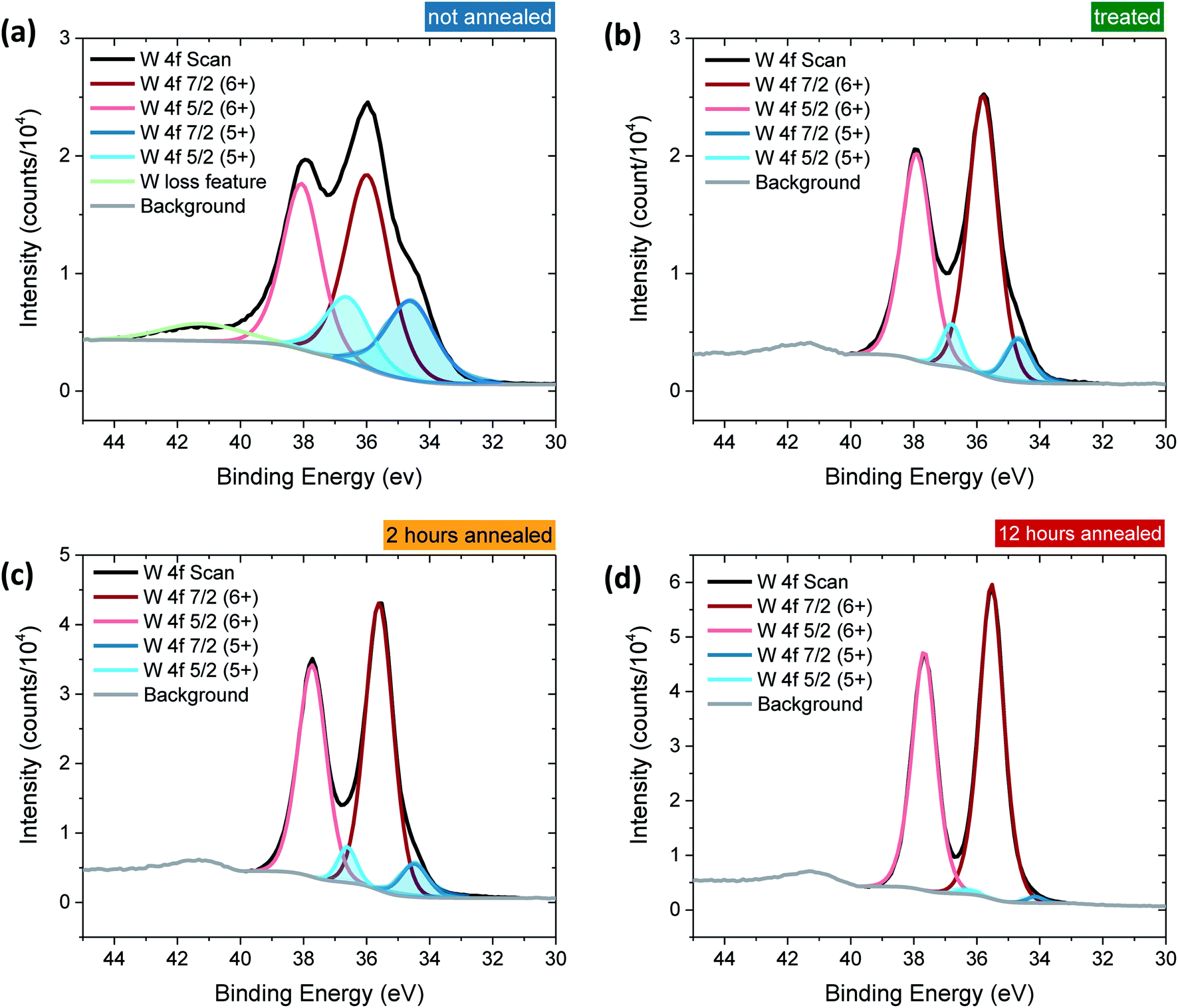 | ||
| Fig. 2 Close up of the W 4f binding region. The 4f doublet is evident in each case from the two spin states (7/2 and 5/2). The main peaks (red) stem from W6+ absorption whereas the smaller shoulders in blue are due to W5+ formed from neighbouring oxygen vacancies (VO). (a) Not annealed (very high [VO], blue), (b) treated (high [VO], green), (c) 2 hours annealed (medium [VO], yellow), and (d) 12 hours annealed (low [VO], red). The ratio of W5+:W6+ (blue:red peaks) clearly decreases from (a) to (d), indicating that fewer oxygen vacancies are present, where W5+:W6+ = (a) 0.35, (b) 0.14, (c) 0.12, (d) 0.03. | ||
| WO3 sample | W5+:W6+ ratio from XPS |
[VO] as % stoichiometric O |
|---|---|---|
| Very high | 0.35 | 5.8% |
| High | 0.14 | 2.3% |
| Medium | 0.12 | 2.0% |
| Low | 0.03 | 0.5% |
The photocurrent performance of each of the films was tested, as shown in Fig. 3, using a 3-electrode cell (see ESI† for details). Strikingly, the photocurrent onset is similar for each [VO] type at ∼0.5 VRHE, but the current plateau is markedly different. The film with ‘very high’ [VO] gives no photocurrent (blue trace), demonstrating metal-like behaviour, but the current progressively increases as the defect concentration is reduced, with the highest photocurrent of 0.45 mA cm−2 at 1.23 VRHE for the ‘medium’ [VO] WO3 (yellow trace). However, as the defect concentration is decreased further still, the current drops again (red trace), thereby indicating that an intermediate doping density results in the best performance. The same ‘pyramidal’ trend can be seen in maximum photocurrent plateaus in Fig. S5† for an alternative sample set, as well as in incident photon-to-current efficiency (IPCE) data at 1.23 VRHE (Fig. S6†). When FTO absorption is accounted for, back-side illumination results in a higher external quantum efficiency than front-side illumination for each sample type, though the difference is more extreme for the sample with ‘low’ [VO]. This pyramidal trend in performance with altered oxygen vacancy concentration has been observed previously in ZnFe2O4 but not in the most common oxides for water oxidation.43 The poor performance of ‘low’ [VO] samples indicates that electron transport is more limiting than hole transport in these nanostructured films, as observed previously,42 and is particularly poor in the ‘low’ [VO] films, indicative of electron conductivity issues as a result of low donor density.
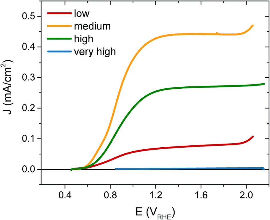 | ||
| Fig. 3 Photocurrent responses for each WO3 sample under simulated 1 sun illumination from the front side in 0.1 M H2SO4, scan rate 10 mV s−1. Data given for ‘very high’ [VO] (blue), ‘high’ [VO] (green), ‘medium’ [VO] (yellow) and ‘low’ [VO] (red). | ||
To further confirm that the trends in performance observed were due to variations only in oxygen vacancy content, we annealed the ‘low’ and ‘medium’ [VO] samples in a reducing atmosphere (10% H2) to add oxygen vacancies back into the samples. Fig. S7† shows that the performance of the poorly doped sample increased after this treatment while the best performing sample gave less photocurrent following H2 annealing as the concentration of oxygen vacancies then surpassed the optimum.
In previous transient optical studies of WO3 needles, we have shown that photogenerated electrons (W5+ species) may be monitored optically by their absorption at 800 nm, in agreement with the W5+ absorption shown in Fig. 1.42 Using transient optical spectroscopy, we monitored the decay of this electron signal for each sample, held at 1.23 VRHE, following pulsed laser excitation across the band-gap, as presented in Fig. 4. Data for the ‘very high’ [VO] sample is not of interest as there is no photocurrent for water oxidation and the film self-oxidises under applied bias, and as such was not studied further herein. We simultaneously measured the transient charge produced at the FTO back contact as a result of electron extraction, which is given by the dashed lines. It is apparent that the highest initial absorption was seen for films with ‘medium’ [VO] – the films that produced the highest photocurrent (Fig. 2). It is equally evident that the rate of decay of this signal matches the rise in the transient charge measured externally, confirming the assignment of the transient absorption signal to photogenerated electrons and indicating that predominantly electron extraction, rather than recombination, is monitored at these times (∼μs to s) and under these conditions. By comparison, both the ‘high’ [VO] sample (green) and the ‘low’ [VO] sample (red) give a smaller initial optical amplitude and less accumulated charge over the same time-window, in agreement with the trend in photocurrent shown in Fig. 3. The smaller initial amplitude of the optical signals for the high and low doped samples suggests that the differences in photocurrent performance are, in part, determined by processes occurring before 10 microseconds. However, the drop in final charge extracted in these samples is quantitatively larger than the variation in initial optical signal, indicating enhanced carrier losses during electron extraction in both the ‘high’ and ‘low’ [VO] samples.
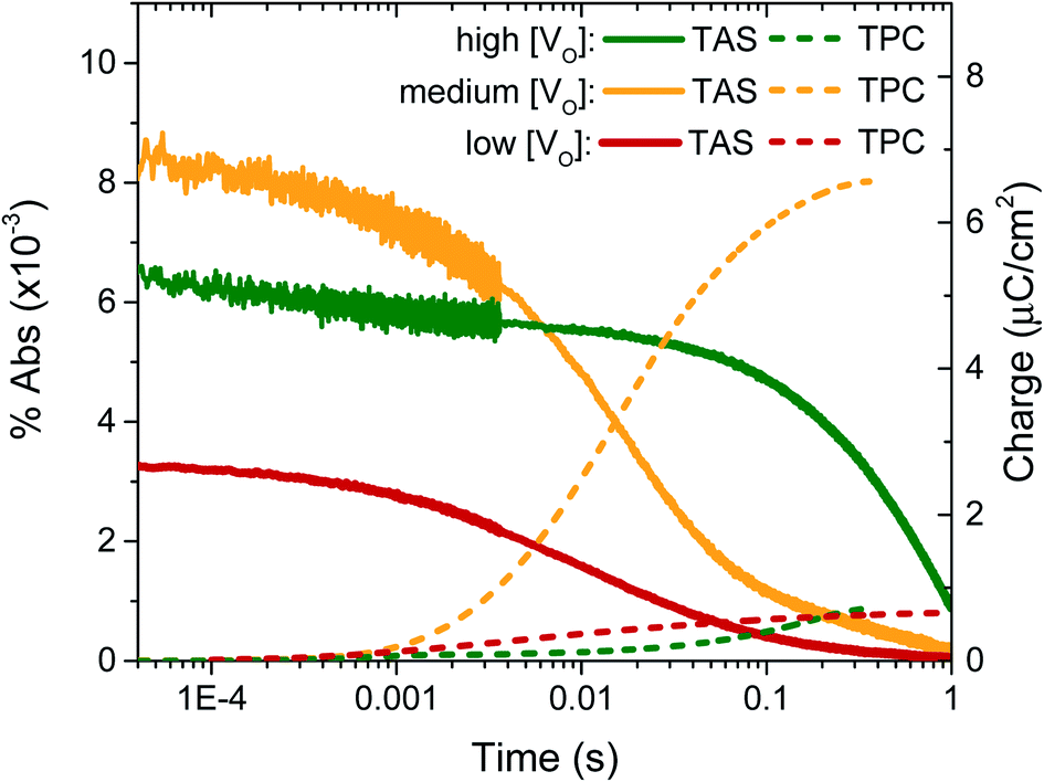 | ||
| Fig. 4 Electron decays (solid lines, 800 nm) under bias (1.23 VRHE) from transient diffuse reflectance spectroscopy measurements in 0.1 M H2SO4, exciting at 355 nm with 0.25 mJ cm−2. The transient photocurrent was measured simultaneously and then integrated to give the transient charge collected (dashed lines). The high performing sample with ‘medium’ doping (yellow) is compared to samples of ‘high’ (green) and ‘low’ doping (red). | ||
The kinetic data in Fig. 4 also indicate that the kinetics of electron extraction are dependent on oxygen vacancy density. The ‘high’ [VO] sample shows a much slower electron decay with a concomitantly slower charge extraction (optical t50% ∼ 0.340 s) compared to the medium [VO] sample (t50% ∼ 0.014 s), whereas the ‘low’ [VO] sample exhibits the fastest kinetics (t50% ∼ 0.009 s) (see also normalised in Fig. S8† and summary in Table 2). This not only confirms that states associated with oxygen vacancies are directly involved in charge transport, as indicated previously,42 but also reveals a direct correlation of VO density with effective electron mobility, with a greater number of vacancies resulting in slower electron extraction, attributed to reversible electron trapping on ionised oxygen vacancy sites. We note this trend is in contrast to the increase in conductivity expected from a greater doping density, as we discuss in more detail below.
| WO3 sample | Optical t50% | TPC t50% |
|---|---|---|
| High | 0.340 s | ∼0.1 s |
| Medium | 0.014 s | 0.016 s |
| Low | 0.009 s | 0.007 s |
To determine the origin of the variation in photogenerated electron yields observed in Fig. 4 at 10 μs, we monitored the electron kinetics on faster timescales (ps to ns timescale) under otherwise comparable conditions, as shown, normalised, in Fig. 5. In previous work, we have shown that two extremes in oxygen vacancy concentration result in very different ultrafast electron kinetics in inert atmosphere,22 but how these kinetics manifest in active samples examined under operando water oxidation conditions was not examined. Once again, herein, significant differences can be observed between the ‘high’, ‘medium’ and ‘low’ VO doped samples. Most notably, the ‘medium’ [VO] sample shows the slowest electron decay, with a greater number of charges remaining at 6 ns, consistent with initial signal amplitudes in Fig. 4 above. Both ‘high’ and ‘low’ concentrations of VO states result in signals that decay faster, indicating that both excessively high and low oxygen vacancy densities can result in greater charge recombination losses on ultrafast timescales, which correlate directly with the yields of long lived charge carriers and photocurrent densities measured under anodic bias.
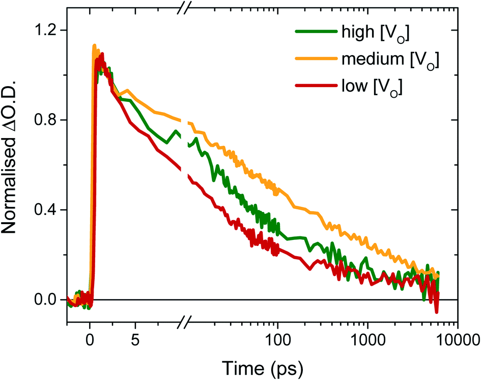 | ||
| Fig. 5 Normalised ultrafast transient absorption kinetics in 0.1 M H2SO4, probing the electron decay at 700 nm from ∼200 femtoseconds to 6 ns after excitation with 355 nm (0.2 mJ cm−2, no bias) for ‘high’ to ‘medium’ and ‘low’ [VO] doping concentrations. | ||
Discussion
As interest in the modulation of intrinsic defects, such as oxygen vacancy states, to enhance photoelectrochemical water splitting performance has heightened,41,44 the need to understand their role in photocurrent generation has become increasingly apparent. Notably, from our J–V data presented in Fig. 3, we find that the maximum photocurrent in our nanostructured WO3 does not correlate with either the highest or lowest concentration of oxygen vacancies studied herein ([VO] ∼ 5.8% and 0.5% respectively) but with an intermediate value, equating to an oxygen vacancy density of ca. 2% of stoichiometric oxygen content. This indicates that these intrinsic defects can enhance performance, but that there is a limit to this enhancement beyond which additional oxygen vacancy states are detrimental. This result affords a bridge between the seemingly contradictive results found at present in the literature on the influence of oxygen vacancies in such metal oxide photoanodes, with both positive17,31,33,43,45–47 and negative34,36,48,49 trends with increasing defects now plausible in different defect density regimes.Front and back IPCE data shown in Fig. S6† also follows the same pyramidal trend in photocurrent generation with increasing oxygen vacancy concentration, as the ‘medium’ [VO] films show the greatest external quantum yields. This can, to some extent, be rationalised as an effect of improved conductivity from increased doping, as proposed by others.31,32,43 In particularly, this provides a plausible explanation for the disparity between front and back illumination currents in the ‘low’ [VO] sample, for which the iR loss resultant from low conductivity may have become a significant factor. However, conductivity arguments cannot be used to rationalise the drop in IPCE with further increases in doping. In earlier work, we demonstrated that oxygen vacancies have a role in electron transport through the WO3 nanostructure,42 and the decay kinetics shown herein (Fig. 4 and 5) further emphasize that these chemical defects have a strong influence on carrier mobility and recombination kinetics. Interestingly, two different effects of oxygen vacancies of the electron dynamics can be discerned, with each dominating on a different timescale. In Fig. 4, we find the initial optical amplitude of the electron signal for each sample correlates with the trend in photocurrent (Fig. 3). As the optical amplitude is proportional to the number of species, the smaller amplitude in samples with ‘high’ or ‘low’ defect state concentrations indicates the presence of fewer photogenerated electrons on these timescales, thereby suggesting an effect of oxygen vacancies on electron loss (recombination) at early times. We discuss this effect further below. The other effect of these vacancy states is apparent at later times in Fig. 4, and in the normalised data in Fig. S8.† As the concentration of defects is increased from ‘low’ to ‘high’, we observe a 100-fold decrease in the electron decay rate and, in accordance, a slower extraction of charge (Fig. S8,† dashed lines). This trend clearly exemplifies the trap-mediated electron transport mechanism proposed previously,42 with increasing numbers of vacancy states limiting the electron mobility due to electron trapping on ionised vacancy sites. Similar changes to transport time have been shown to result from applied bias, with higher anodic bias increasing the number of available trap-sites by modulating oxygen-vacancy state occupancy, thereby slowing electron extraction.42 The low mobility in highly doped samples also incurs a penalty on the performance, with both the quantum yield (determined from IPCE data) and the extracted charge (determined from integrated photocurrent transients) dropping relative to the ‘medium’ doped sample by significantly more than the variation in photogenerated electron density (optical signal) measured at 10 μs (Table S1†). In other words, not all of the electrons observed on slow timescales in ‘high’ [VO] samples are contributing to current, with the large number of defects likely invoking trap-mediated recombination during electron extraction, as suggested by others.34,37,43 Considering the nanoneedle nature of these films, electron transport will proceed in close proximity to holes accumulating at the WO3 surface, such that recombination losses during extraction are plausible, as depicted in Scheme 1.
 | ||
| Scheme 1 (Upper) Illustration of a single nanoneedle of WO3 (yellow) on FTO (grey), indicating electron (black) transport (black arrows) and possible recombination pathways with holes (white) on route to extraction. (Lower) Indication of the dominant kinetic pathways immediately following charge separation in each of the samples examined; ‘very high’ [VO] (left, blue), ‘high’ [VO] (centre left, green), ‘medium’ [VO] (centre right, yellow) and ‘low’ [VO] (right, red). Arrow weight depicts likelihood of event. Filled VO states are given in colour, empty states able to trap electrons are given in yellow. ‘Very high’ [VO] shows hole trapping faster than instrument detection (heavy arrow). The ‘high’ doped sample has the greatest bulk trap recombination, particularly from hole trapping, so later carrier collection is limited. With too few defect states (‘low’, red), charge separation is hindered and the probability of geminate and bimolecular recombination increases. The best performing sample has the optimal amount of defects to aid charge separation without losing carriers to trap-mediated recombination. | ||
In contrast to the highly doped sample, the ‘low’ [VO] sample presents a faster electron decay on μs to s timescales and earlier charge extraction (Fig. 4). Once again, this can be rationalised by considering electron transport through the WO3 nanoneedle: with fewer oxygen vacancy sites in the sample (and the atomic distance between those remaining likely larger), electrons will go through fewer trapping and de-trapping steps before reaching the back contact and are therefore extracted faster. Furthermore, the ‘low’ [VO] sample is expected to exhibit a wider space-charge layer as a result of its lower doping density, which may also contribute to faster extraction as a greater proportion of photogenerated electrons can be expected to experience drift fields, driving more of them to the centre of the rod where they may shield one-another. However, the extraction efficiency remains low for this film, as indicated by the quantum yield, which could be due to increased ‘free carrier’ recombination as a result of inadequate trapping and localisation. This positive contribution of electron trapping to performance has seldom been considered in previous studies examining variations in oxygen vacancy concentration.43
As discussed above, the initial electron population observed in Fig. 4 is determined by loss processes occurring on earlier timescales. The ultrafast carrier dynamics for these samples, normalised for ease of comparison, are shown in Fig. 5. Strikingly, we observe significant differences in electron decay kinetics between the samples from just a couple of picoseconds after excitation. As predicted from the optical signal in the slow data (Fig. 4), the ‘low’ [VO] sample shows the fastest decay on ultrafast timescales, indicating greater bulk recombination losses, which eventually result in the poor photocurrent observed for this sample (Fig. 3). Similarly, the ‘high’ [VO] sample also shows faster recombination kinetics than the best performing sample. Since charge separation and geminate and non-geminate recombination processes dominate the kinetics at these timescales, it can be concluded that oxygen vacancy states are affecting these processes. Moreover, it can be determined that the nature of their effect on charge longevity must be both beneficial and detrimental, as an intermediate number of vacancies still produces the best performance. Firstly, a detrimental effect of increasing defect concentration is observed going from ‘medium’ to ‘high’ [VO], which we largely assign to the trapping of photogenerated valence-band holes into filled oxygen vacancy states, in excess in this sample. This assignment stems from our previous observations that a very high population of occupied defect states (those below the Fermi level) results in bulk hole trapping within 300 femtoseconds, leading to a loss in the W5+ absorption from electrons in these states.22,28 Indeed, the non-normalised data reveals a smaller initial amplitude for the higher doped sample, indicative of electron loss from rapid hole trapping (Fig. S10†). This assignment is also supported by Fig. S9,† which reveals that ultrafast kinetics of the highest doped sample, ‘very high’ [VO], show only a negative signal (bleach) at the same examined wavelength, due to a transient loss, rather than gain, of trapped electrons, corroborating previous ultrafast results performed in inert atmosphere.22 Holes that trap deeply or recombine with electrons are unable to contribute to water oxidation, and thus higher incidences of trap-assisted recombination result in lower photocurrents. In the extreme case of the very highly doped sample, the overwhelming degree of hole trapping from early times results in no photocurrent at all for water oxidation (Fig. 3).
The beneficial effect of intermediate oxygen vacancy densities on early timescale processes is arguably more surprising. When comparing the electron kinetics of the ‘low’ [VO] sample with ‘medium’ [VO], we observe a retardation of bulk recombination in the latter, which cannot easily be rationalised as a reduction in charge trapping, considering the ‘medium’ [VO] sample is more doped. It appears more likely that the retarded recombination losses of this ‘medium’ doped sample over the ‘low’ doped sample arises from improved charge separation as a result of enhanced electron localisation on ionised oxygen vacancy sites. In other words, the relative absence of oxygen vacancy states in the ‘low’ [VO] sample could be expected to increase the proportion of mobile electrons in the conduction band, accelerating their recombination with valence band holes. This free-electron–hole recombination could account for the lower electron amplitude at 0.2 ps in the ‘low’ [VO] sample (Fig. S10†) and also reconcile the faster electron decay across the entire ultrafast window, as electrons will spend proportionally more time moving between trap states due to there being fewer of them. This stands in contrast to the oxygen vacancy study on ZnFe2O4, which attributes the poor performance of lower [VO] solely to reduced conductivity.43 The idea of improved charge separation through carrier trapping has been proposed previously in other materials,50,51 but has not been observed directly, to the best of our knowledge, in the most common oxide photoanodes for water oxidation. For example, in their examination of Zr–Bi2WO6 for organic photodegradation reactions, Zhang et al. determine that ‘an appropriate’ oxygen vacancy leads to the temporary trapping of photogenerated electrons, thereby enhancing charge separation.52 This reversible electron trapping that we observe herein, even from pre-picosecond timescales, may thus be applicable to many similar photoanodes for a multitude of applications. As such, the vital role of these intrinsic defect states in early-time processes such as charge separation in these materials cannot be overstated, and cannot be adequately described by comparison of two extremes.22,53,54 The role of oxygen vacancies in charge separation and electrons transport in WO3, from femtoseconds to seconds, is summarised in Scheme 1.
Whether the trends with varied oxygen vacancy concentration reported herein are specific to WO3 as a product of this material's infamously high doping densities, or are general to all metal oxides cannot be concluded from this study alone. For example, Forster et al. have shown there to be a fine balance between enhanced electrical properties and trap-mediated losses in α-Fe2O3 films with high oxygen vacancy densities. However, they concluded that there was no significant enhancement in initial charge separation with the addition of VO, (comparing only two doping densities) and focused solely on slow timescales, so the complete effects of oxygen vacancies on the initial charge separation in hematite remain unclear.53 Further studies are required to elucidate whether the optimum oxygen vacancy concentration is similar between different metal oxides, and whether all equally benefit from enhanced carrier trapping (rather than simply increased conductivity). Likewise, the nanostructured nature of these samples, while known to be key to enhanced performance, may also play a negative role in enabling recombination with surface holes at later times during electron extraction parallel to the nanorod surface; in a dense film such losses would be less important due to electron extraction proceeding perpendicular to film surface (Scheme 1, upper). Nonetheless, nanostructuring and doping are commonly employed tools for the betterment of many photoanode materials, and as such, balancing the positive and negative attributes of VO states highlighted herein may be paramount to achieving maximum quantum yields in a large number of current and still-to-be-developed materials for solar fuels applications.
Contributions
Conceptualisation, S. C., L. F., J. D.; resources, S. C., A. K.; investigation, S. C.; writing, S. C.; visualisation, S. C.; supervision, L. F., J. D.; funding acquisition, J. D.Conflicts of interest
The authors declare no competing interests.Acknowledgements
J. R. D. acknowledges financial support from the European Research Council (project Intersolar 291482). This project has received funding from the European Union's Horizon 2020 research and innovation program under grant agreement 732840-A-LEAF. S. C. would like to thank Imperial College for a Schrödinger Scholarship. L. F. thanks the EU for a Marie Curie fellowship (658270) and A. K. thanks Imperial College for a Junior Research Fellowship and the Royal Society for a Research Grant (RSG\R1\180434).References
- F. E. Osterloh, Chem. Mater., 2008, 20, 35–54 CrossRef CAS.
- I. Roger, M. A. Shipman and M. D. Symes, Nat. Rev. Chem., 2017, 1, 1–14 CrossRef.
- Z. F. Huang, J. Song, L. Pan, X. Zhang, L. Wang and J. J. Zou, Adv. Mater., 2015, 27, 5309–5327 CrossRef CAS PubMed.
- Z.-F. Huang, L. Pan, J.-J. Zou, X. Zhang and L. Wang, Nanoscale, 2014, 6, 14044–14063 RSC.
- B. D. Alexander, P. J. Kulesza, I. Rutkowska, R. Solarska and J. Augustynski, J. Mater. Chem., 2008, 18, 2298–2303 RSC.
- J. K. Hurst, Science, 2010, 328, 315–316 CrossRef CAS PubMed.
- X. Wang, K. Maeda, A. Thomas, K. Takanabe, G. Xin, J. M. Carlsson, K. Domen and M. Antonietti, Nat. Mater., 2008, 8, 76 CrossRef PubMed.
- S. Ghosh, N. A. Kouamé, L. Ramos, S. Remita, A. Dazzi, A. Deniset-Besseau, P. Beaunier, F. Goubard, P.-H. Aubert and H. Remita, Nat. Mater., 2015, 14, 505 CrossRef CAS PubMed.
- P. Bornoz, M. S. Prévot, X. Yu, N. Guijarro and K. Sivula, J. Am. Chem. Soc., 2015, 137, 15338–15341 CrossRef CAS PubMed.
- J. Tao, T. Luttrell and M. Batzill, Nat. Chem., 2011, 3, 296 CrossRef CAS PubMed.
- M. Grzelczak, J. Zhang, J. Pfrommer, J. Hartmann, M. Driess, M. Antonietti and X. Wang, ACS Catal., 2013, 3, 383–388 CrossRef CAS.
- R. P. Forslund, W. G. Hardin, X. Rong, A. M. Abakumov, D. Filimonov, C. T. Alexander, J. T. Mefford, H. Iyer, A. M. Kolpak, K. P. Johnston and K. J. Stevenson, Nat. Commun., 2018, 9, 3150 CrossRef PubMed.
- K. Song, Z. Ma, W. Yang, H. Hou and F. Gao, J. Mater. Sci.: Mater. Electron., 2018, 29, 8338–8346 CrossRef CAS.
- M. D. L. Balela, R. A. Acedera, C. L. I. Flores and C. M. O. Pelicano, Surf. Coat. Technol., 2018, 340, 199–209 CrossRef CAS.
- X. Li, J. Wei, Q. Li, S. Zheng, Y. Xu, P. Du, C. Chen, J. Zhao, H. Xue, Q. Xu and H. Pang, Adv. Funct. Mater., 2018, 28, 1800886 CrossRef.
- A. Kafizas, L. Francàs, C. Sotelo-Vazquez, M. Ling, Y. Li, E. Glover, L. McCafferty, C. Blackman, J. Darr and I. Parkin, J. Phys. Chem. C, 2017, 11, 5983–5993 CrossRef.
- R. Zhang, F. Ning, S. Xu, L. Zhou, M. Shao and M. Wei, Electrochim. Acta, 2018, 274, 217–223 CrossRef CAS.
- C. Di Valentin and G. Pacchioni, Acc. Chem. Res., 2014, 47, 3233–3241 CrossRef CAS PubMed.
- M. T. Greiner, L. Chai, M. G. Helander, W.-M. Tang and Z.-H. Lu, Adv. Funct. Mater., 2012, 22, 4557–4568 CrossRef CAS.
- F. Mehmood, R. Pachter, N. R. Murphy, W. E. Johnson and C. V. Ramana, J. Appl. Phys., 2016, 120, 233105 CrossRef.
- D. B. Migas, V. L. Shaposhnikov, V. N. Rodin and V. E. Borisenko, J. Appl. Phys., 2010, 108, 093713 CrossRef.
- M. Sachs, J.-S. Park, E. Pastor, A. Kafizas, A. A. Wilson, L. Francàs, S. Gul, M. Ling, C. Blackman, J. Yano, A. Walsh and J. R. Durrant, Chem. Sci., 2019, 10, 5667–5677 RSC.
- S. K. Deb, Sol. Energy Mater. Sol. Cells, 2008, 92, 245–258 CrossRef CAS.
- A. Naldoni, M. Allieta, S. Santangelo, M. Marelli, F. Fabbri, S. Cappelli, C. L. Bianchi, R. Psaro and V. Dal Santo, J. Am. Chem. Soc., 2012, 134, 7600–7603 CrossRef CAS PubMed.
- X. Zhao, J. Feng, S. Chen, Y. Huang, T. C. Sum and Z. Chen, Phys. Chem. Chem. Phys., 2017, 19, 1074–1082 RSC.
- F. M. Pesci, G. Wang, D. R. Klug, Y. Li and A. J. Cowan, J. Phys. Chem. C, 2013, 117, 25837–25844 CrossRef CAS PubMed.
- F. Wang, C. Di Valentin and G. Pacchioni, Phys. Rev. B: Condens. Matter Mater. Phys., 2011, 84, 073103 CrossRef.
- S. Corby, E. Pastor, Y. Dong, X. Zheng, L. Francàs, M. Sachs, S. Selim, A. Kafizas, A. A. Bakulin and J. R. Durrant, J. Phys. Chem. Lett., 2019, 5395–5401, DOI:10.1021/acs.jpclett.9b01935.
- A. M. Smith, M. G. Kast, B. A. Nail, S. Aloni and S. W. Boettcher, J. Mater. Chem. A, 2014, 2, 6121–6129 RSC.
- G. Wang, H. Wang, Y. Ling, Y. Tang, X. Yang, R. C. Fitzmorris, C. Wang, J. Z. Zhang and Y. Li, Nano Lett., 2011, 11, 3026–3033 CrossRef CAS PubMed.
- G. Wang, Y. Ling and Y. Li, Nanoscale, 2012, 4, 6682–6691 RSC.
- G. Liu, J. Han, X. Zhou, L. Huang, F. Zhang, X. Wang, C. Ding, X. Zheng, H. Han and C. Li, J. Catal., 2013, 307, 148–152 CrossRef CAS.
- G. Wang, Y. Ling, H. Wang, X. Yang, C. Wang, J. Z. Zhang and Y. Li, Energy Environ. Sci., 2012, 5, 6180–6187 RSC.
- M. B. Johansson, A. Mattsson, S.-E. Lindquist, G. A. Niklasson and L. Österlund, J. Phys. Chem. C, 2017, 121, 7412–7420 CrossRef CAS.
- M. B. Johansson, P. T. Kristiansen, L. Duda, G. A. Niklasson and L. Österlund, J. Phys.: Condens. Matter, 2016, 28, 475802 CrossRef CAS PubMed.
- H. Wang, T. Lindgren, J. He, A. Hagfeldt and S.-E. Lindquist, J. Phys. Chem. B, 2000, 104, 5686–5696 CrossRef CAS.
- M. Kong, Y. Li, X. Chen, T. Tian, P. Fang, F. Zheng and X. Zhao, J. Am. Chem. Soc., 2011, 133, 16414–16417 CrossRef CAS PubMed.
- T. Leshuk, R. Parviz, P. Everett, H. Krishnakumar, R. A. Varin and F. Gu, ACS Appl. Mater. Interfaces, 2013, 5, 1892–1895 CrossRef CAS PubMed.
- T.-H. Xie and J. Lin, J. Phys. Chem. C, 2007, 111, 9968–9974 CrossRef CAS.
- J. Wang, D. N. Tafen, J. P. Lewis, Z. Hong, A. Manivannan, M. Zhi, M. Li and N. Wu, J. Am. Chem. Soc., 2009, 131, 12290–12297 CrossRef CAS PubMed.
- X. Pan, M.-Q. Yang, X. Fu, N. Zhang and Y.-J. Xu, Nanoscale, 2013, 5, 3601–3614 RSC.
- S. Corby, L. Francàs, S. Selim, M. Sachs, C. Blackman, A. Kafizas and J. R. Durrant, J. Am. Chem. Soc., 2018, 140, 16168–16177 CrossRef CAS PubMed.
- J. H. Kim, Y. J. Jang, J. H. Kim, J.-W. Jang, S. H. Choi and J. S. Lee, Nanoscale, 2015, 7, 19144–19151 RSC.
- J. Wang, R. Chen, L. Xiang and S. Komarneni, Ceram. Int., 2018, 44, 7357–7377 CrossRef CAS.
- Y. Li, Z. Tang, J. Zhang and Z. Zhang, J. Alloys Compd., 2017, 708, 358–366 CrossRef CAS.
- Y. Ling, G. Wang, H. Wang, Y. Yang and Y. Li, ChemSusChem, 2014, 7, 848–853 CrossRef CAS PubMed.
- T.-Y. Yang, H.-Y. Kang, U. Sim, Y.-J. Lee, J.-H. Lee, B. Koo, K. T. Nam and Y.-C. Joo, Phys. Chem. Chem. Phys., 2013, 15, 2117–2124 RSC.
- R. Katoh, A. Furube, K.-i. Yamanaka and T. Morikawa, J. Phys. Chem. Lett., 2010, 1, 3261–3265 CrossRef CAS.
- M. Barroso, S. R. Pendlebury, A. J. Cowan and J. R. Durrant, Chem. Sci., 2013, 4, 2724–2734 RSC.
- H. Yu, J. Li, Y. Zhang, S. Yang, K. Han, F. Dong, T. Ma and H. Huang, Angew. Chem., Int. Ed., 2019, 58, 3880–3884 CrossRef CAS PubMed.
- S. A. Ansari, M. M. Khan, S. Kalathil, A. Nisar, J. Lee and M. H. Cho, Nanoscale, 2013, 5, 9238–9246 RSC.
- Z. Zhang, W. Wang, E. Gao, M. Shang and J. Xu, J. Hazard. Mater., 2011, 196, 255–262 CrossRef CAS PubMed.
- M. Forster, R. J. Potter, Y. Ling, Y. Yang, D. R. Klug, Y. Li and A. J. Cowan, Chem. Sci., 2015, 6, 4009–4016 RSC.
- J. J. M. Vequizo, S. Nishioka, J. Hyodo, Y. Yamazaki, K. Maeda and A. Yamakata, J. Mater. Chem. A, 2019, 7, 26139–26146 RSC.
Footnote |
| † Electronic supplementary information (ESI) available. See DOI: 10.1039/c9sc06325k |
| This journal is © The Royal Society of Chemistry 2020 |