
 Open Access Article
 This Open Access Article is licensed under a
 Creative Commons Attribution 3.0 Unported Licence
A sensitive, uniform, reproducible and stable SERS substrate has been presented based on MoS2@Ag nanoparticles@pyramidal silicon
Shouzhen Jiang†
*a,
Jia Guo† a,
Chao Zhanga,
Chonghui Lia,
Minghong Wanga,
Zhen Lia,
Saisai Gaoa,
Peixi Chena,
Haipeng Sib and
Shicai Xuc
a,
Chao Zhanga,
Chonghui Lia,
Minghong Wanga,
Zhen Lia,
Saisai Gaoa,
Peixi Chena,
Haipeng Sib and
Shicai Xuc
aSchool of Physics and Electronics, Shandong Normal University, Jinan 250014, China. E-mail: jiang_sz@126.com
bDepartment of Orthopaedics, Qilu Hospital, Shandong University, 107 Wenhuaxilu Street, Jinan 250012, China
cShandong Provincial Key Laboratory of Biophysics, College of Physics and Electronic Information, Dezhou University, Dezhou 253023, PR China
First published on 18th January 2017
Abstract
By combining the excellent surface-enhanced Raman scattering (SERS) activity of Ag nanoparticles (AgNPs), the well-separated pyramid arrays of the pyramidal silicon (PSi) and unique physical/chemical properties of molybdenum disulfide (MoS2), the MoS2@AgNPs@PSi substrate shows high performance in terms of sensitivity, uniformity, reproducibility and stability. By using rhodamine 6G (R6G) as probe molecule, the SERS results indicate that the MoS2@AgNPs@PSi substrate is superior to the AgNPs@PSi, AgA@PSi (the second annealing of the AgNPs@PSi) and the MoS2@AgNPs@flat-Si substrate. The MoS2@AgNPs@PSi substrate also shows the reasonable linear response between the Raman intensity and R6G concentration. The maximum deviations of SERS intensities from 20 positions on a same MoS2@AgNPs@PSi substrate and 10 MoS2@AgNPs@PSi substrates in different batches are less than 7.6% and 9%, respectively, revealing the excellent uniformity and reproducibility of the substrate. Besides, the SERS substrate has a good stability, the Raman intensity of the MoS2@AgNPs@PSi substrate only drop by 15% in a month. The corresponding experimental and theoretical results suggest that our proposed MoS2@AgNPs@PSi substrate is expected to offer a new and practical way to accelerate the development of label-free SERS detection.
1. Introduction
In recent decades, surface-enhanced Raman scattering (SERS) as a very important analytical technique for molecular detection has received increasing attention.1–3 About SERS, it is now well accepted that the plasmonic coupling effect at the nanometre gap junction between metal particles induces enormous electromagnetic enhancement that allows SERS signal to be detected with high sensitivity.4–8 However, the non homogeneous structure and instability of SERS substrate based on metal nanoparticles restricts the practical application and commercialization of SERS technology.9 An ideal SERS nanostructure for practical applications should induce a high signal enhancement, generate a uniform and reproducible response, and have a long-term stability.10Layered transition metal dichalcogenides (LTMDs) have received much attention due to their remarkable optoelectronic properties.11–13 Molybdenum disulfide (MoS2) belongs to the family of LTMDs. The layered MoS2 has unique physical, optical and electrical properties, making it very interesting for applying as a promising supporting material to stabilize metal nanoparticles, forming hierarchical composites.14–17 The composites (MoS2/metal nanoparticles) sometimes offer synergistic effects to the intrinsic properties of the metal nanoparticles, making the composites much more attractive in applications of surface-enhanced Raman scattering (SERS) than the metal nanoparticles alone.18,19 Compared with graphene, MoS2 can be get in a low temperature that can effectively reduce energy consumption and makes it easily combine with a traditional metallic substrate,20–24 which allows us to take advantage of both electromagnetic mechanism (EM) and a chemical mechanism (CM). In our work, we directly grew MoS2 on Ag nanoparticles (AgNPs) by thermally decomposing the precursor of (NH4)2MoS4. The MoS2 films exhibits three advantages in our work: first, the MoS2 films can provide the chemical enhancement and efficient adsorption for various target molecules, so the sensitivity of the substrate is enhanced; second, the MoS2 layer reduces the additional signal by isolating the metal nanoparticles from the R6G molecules. This characteristic of MoS2 will enhance the uniformity of SERS signals; third, the MoS2 films can isolate AgNPs from surrounding environment, effectively protect AgNPs from oxidation and endow the hybrid system a good stability and long lifetime. Thus a sensitive, uniform and stable SERS substrate is to be formed.
In order to further enhance the sensitivity of the detection of Raman signals, porous Si has been intensively chosen to serve as SERS active substrate in recent years.25–29 It has been demonstrated that porous Si possessing large specific area and governable nanoporous structure can effective increase the number of hot spots and further enhance the sensitivity of the SERS signals. So all kinds of methods including laser interference lithography,30 chemical method,31 metal-assisted chemical etching,32 reactive ion etching33 have been carried out to fabricate the porous Si. The method of laser interference lithography or reactive ion etching can produce well-defined Si nanopattern. However these methods are time-consuming and expensive. Uniform porous Si with small structure can be produced with the chemical method or metal-assisted chemical etching. Although these methods relatively lost-cost, but they require multiple steps and multifarious strong acids in the preparation process. In our work, a relatively simple and lost-cost method was used to obtain the pyramidal Si (PSi) SERS substrate. PSi possessing well-separated pyramid arrays different from the traditional pillar arrays. The scattering area of PSi is very large and the incident laser is able to produce an effective oscillation among the valleys of PSi, which can further enhance the sensitivity of SERS substrate.34,35 Besides, the PSi possessing well-separated pyramid arrays, which can make contribution to the uniformity of the substrate.
Herein, we combine MoS2, AgNPs and PSi forming the MoS2@AgNPs@PSi substrate. By using rhodamine 6G (R6G) as a probe molecule, we experimentally realize and prove the high sensitivity, excellent uniformity and reproducibility and long-term stability of the MoS2@AgNPs@PSi substrate.
2. Experimental
2.1. The preparation of the MoS2@AgNPs@PSi substrate
The preparation processes of the MoS2@AgNPs@PSi substrate are summarized in Fig. 1. We fabricate PSi substrates through wet texturing boron-doped single crystal silicon wafer with the assist of the NaOH solution. Subsequently, all the PSi substrates were cleaned by acetone, alcohol and deionized water in ultrasonic cleaner for 30 min, respectively. By thermal-evaporation system, continuous Ag films was deposited on PSi substrate. In order to obtain appropriate AgNPs, the PSi with Ag films was placed in the quartz tube and the pressure was pumped to 10−3 Pa. Then 40 sccm Ar was introduced into the quartz tube and the temperature has been raised to 500 °C for annealing 30 min. Finally, the temperature of the quartz tube was fast cooled down to room temperature by opening the lid of furnace. Through these steps, the AgNPs@PSi substrate was obtained. The 10 mL dimethylformamide was added into the high purity of (NH4)2MoS4 (purity of 99.99%; 1 g) powder to form a 1 wt% solution. Next, the (NH4)2MoS4 solution was treated by sonication in ultrasonic cleaner for 20 min with the power of 80 W to break down the undissolved particles. The (NH4)2MoS4 solution was immediately deposited on the AgNPs@PSi substrate by using a spin-coating method. In order to get the MoS2@AgNPs@PSi substrate, the thermally decomposing process was performed through the second annealing. First, the (NH4)2MoS4 membrane was placed in the quartz tube and the pressure was pumped to 10−3 Pa. Second, 80 sccm Ar was introduced into the tube and the temperature reached 500 °C for annealing 90 min. Third, the tube was fast cooled down to room temperature by opening the furnace. In order to demonstrate the effect of the MoS2 layer, we also prepared AgA@PSi (the second annealing of the AgNPs@PSi). The AgNPs@PSi substrate without coating (NH4)2MoS4 solution was directly placed in the quartz tube for the second annealing. The AgA@PSi substrate was fabricated with the same method as preparing the MoS2@AgNPs@PSi substrate. Besides, we prepared the MoS2@AgNPs@flat-Si substrate in the same way, to evaluate the role of PSi.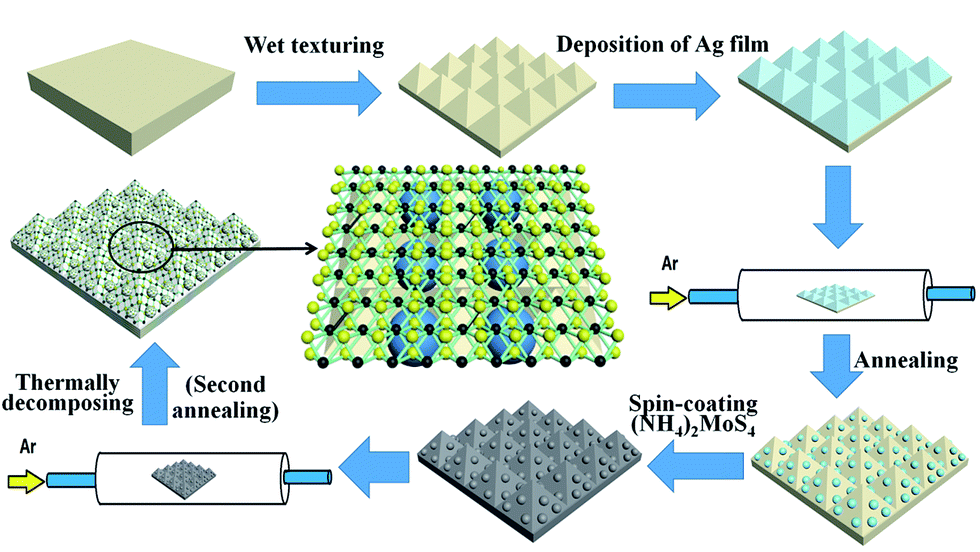 | ||
| Fig. 1 The preparation processes of the MoS2@AgNPs@PSi substrate. | ||
2.2. Apparatus and characterization
Surface morphologies of the MoS2@AgNPs@PSi substrate were observed using scanning electron microscopy (SEM, Zeiss Gemini Ultra-55). The Raman spectroscopy was performed using a Raman spectrometer (Horiba HR Evolution 800) with laser excitation at 532 nm. The crystalline quality and the single-crystalline structure of MoS2 thin films were characterized by XRD (Bruker D8).3. Results and discussion
As shown in Fig. 2(a), (c) and (e), after the texturing process, the samples shows clearly a typical surface morphology of PSi, which is composed of abundant well-separated pyramid arrays. The well-separated pyramid arrays can make contribution to the uniformity of the substrate. As illustrated in Fig. 2(a), well-ordered AgNPs are observed on the PSi substrate, which enables the AgNPs@PSi substrate to have high sensitivity and excellent uniformity. In order to observe more clearly, SEM image under a high magnification was obtained (the red circle in Fig. 2(a) is amplified), the distribution of the AgNPs is much homogeneous on both valley bottom and surface, as shown in Fig. 2(b). From the inset in Fig. 2(b), the average size of the AgNPs is about 35 nm. Fig. 2(c) shows the SEM image of the MoS2@AgNPs@PSi substrate, with the virtue of the direct growth method, the MoS2@AgNPs structure still maintains the well-ordered structure. The red circle in Fig. 2(c) is amplified in order to clearly observe, the size and interparticle distance of MoS2@AgNPs hybrid structure are similar to that of AgNPs in Fig. 2(b), as shown in Fig. 2(d). Fig. 2(e) and (f) are SEM images of the AgA@PSi substrate in different magnification. Obviously, there are many large size of the AgNPs in the valley bottom and surface of PSi. This phenomenon is attributed to the Ostwald ripening effect generated by the second annealing,36 which leads to the occurrence of AgNPs clusters. These particles will greatly weaken the Raman enhancement effect. But for the MoS2@AgNPs@PSi substrate, the persistent high temperature did not make the MoS2@AgNPs hybrid structure produced clusters, probably because the AgNPs were wrapped up by the thin layer of MoS2, and the AgNPs can not fusion. SEM image of the AgNPs@flat-Si substrate is shown in Fig. 2(g). Similar with that of the AgNPs@PSi substrate, the AgNPs on the AgNPs@flat-Si substrate are also well-ordered. The MoS2 layers are also grown on the AgNPs@flat-Si forming the MoS2@AgNPs@flat-Si substrate, as shown in Fig. 2(h). | ||
| Fig. 2 (a) and (b) are SEM images of the AgNPs@PSi substrate in different magnification. (c) and (d) are SEM image of the MoS2@AgNPs@PSi substrate in different magnification. (e) and (f) are SEM images of the AgA@PSi substrate in different magnification. (g) SEM image of the AgNPs@flat-Si substrate. (h) SEM image of the MoS2@AgNPs@flat-Si substrate. | ||
In order to further investigate the distribution of the MoS2 layers, Raman spectra were obtained from the randomly selected twenty points on the MoS2@AgNPs@PSi substrate, as shown in Fig. 3(a). The profile of Raman spectra of MoS2 from different positions is very similar, neither a shift in the characteristic Raman peaks nor a significant change in the Raman intensity occurs, indicating the uniformity of the MoS2 films in the whole substrate. Two Raman characteristic peaks of in-plane vibrational mode E12g and out-of-plane vibrational mode A1g are all clearly seen.37 The full-width-half maximum (FWHM) values of E12g and A1g band respectively are 3–4 and 5–7 cm−1. The peak frequency difference (Δ) between E12g and A1g Raman modes can be used to identify the layer number of MoS2.37 The value of Δ is obtained from the Raman spectra of MoS2 in Fig. 3(a). As shown in Fig. 3(b), the values of Δ are in the range of 20–22 cm−1, which indicate that the as-grown MoS2 are 2–3 layers. In order to further demonstrate the uniformity of the MoS2 film, the 10 × 10 μm2 Raman mappings are obtained as shown in Fig. 3(c) and (d). The small color variations show favorable stability of the E12g and A1g Raman modes, indicating that the substrate is almost covered with MoS2 layers. Fig. 3(e) shows EDS spectra from the MoS2@AgNPs@PSi substrate. The peaks associated with silicon, silver, sulfur and molybdenum are clearly observed. This shows that the MoS2@AgNPs@PSi substrate is successfully prepared. Fig. 3(f) shows in-plane X-ray diffraction (XRD) pattern of the MoS2@AgNPs@PSi substrate. The three strikingly peaks at 31.910, 69.016 and 69.158° assigned as (100), (200) and (108) of the MoS2 crystals separately (powder diffraction fille (PDF) no. 751539). The diffraction peaks at 38.116 and 44.277 degree is attributed to the (111) and (200) crystal planes of AgNPs (powder diffraction fille (PDF) no. 04-0783). Based on the above mentioned images, we preliminary draw a conclusion that the MoS2 layers have successfully wrap the AgNPs and PSi.
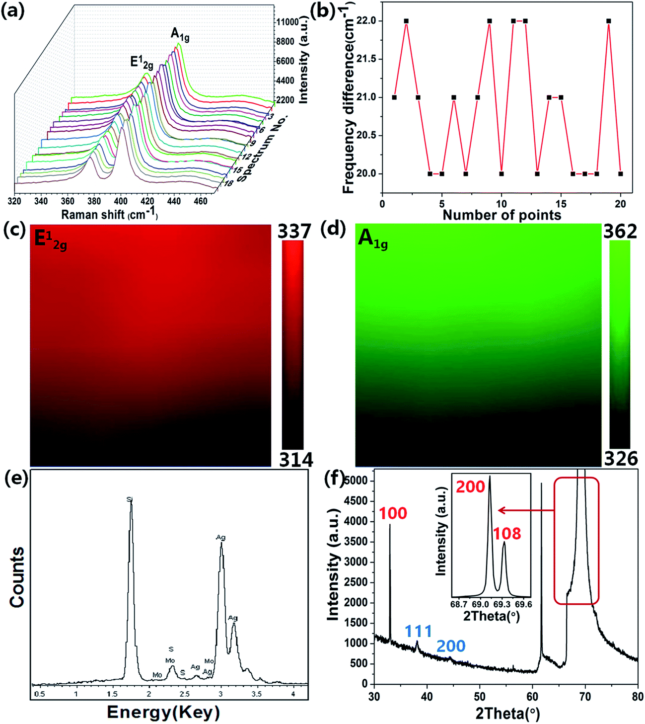 | ||
| Fig. 3 (a) Raman spectra of the MoS2 layers from the MoS2@AgNPs@PSi substrate. (b) The calculated peak frequency difference (Δ) between E12g and A1g Raman modes according to the Raman spectra in (a). (c) and (d) are Raman mapping of E12g and A1g peaks of MoS2, respectively. (e) EDS spectra of the MoS2@AgNPs@PSi substrate. (f) XRD pattern of the MoS2@AgNPs@PSi substrate. | ||
Fig. 4(a) shows the TEM image of the MoS2@AgNPs structure, we can see that the size of the MoS2@AgNPs structure is uniform. In order to clearly observe the MoS2 layers on the surface of the AgNPs, TEM image under a high magnification was obtained. As shown in Fig. 4(b), with the virtue of the direct growth method, the MoS2 layers tightly wrap the AgNPs, minimizing the loss of electromagnetic enhancement activity and endow the MoS2@AgNPs@PSi substrate a high sensitivity. From the red circles in Fig. 4(b), the AgNPs were covered with two layer (above) or three layer (below) MoS2 can be clearly observed.
 | ||
| Fig. 4 (a) TEM image of the MoS2@AgNPs structure. (b) TEM image of the MoS2@AgNPs structure in high magnification. | ||
To estimate the SERS activity of the MoS2@AgNPs@PSi substrate, we compared the behaviors of MoS2@AgNPs@PSi substrate with that of AgNPs@PSi, AgA@PSi and MoS2@AgNPs@flat-Si substrate. The R6G molecules with varied concentrations were chosen as the probe molecule and all the SERS spectra were implemented on the same conditions. The main Raman enhancement peaks of R6G are 612, 773, 1185, 1311, 1362, 1506, 1570 and 1647 cm−1.38,39 The measured SERS intensity decay with the decrease of the R6G concentration for all prepared substrates. Through comparison of Fig. 5(a) and (b) we can see that the minimum detected concentration of R6G from the MoS2@AgNPs@PSi substrate is one order of magnitude lower than that from the AgNPs@PSi substrate, which can be as low as 10−11 M. The reason for this phenomenon is the CM enhancement effect from MoS2. Besides the MoS2 film also acts as the excellent adsorbent towards organic molecules. From Fig. 5(b) we can also clearly see the E12g and A1g two peaks, which proved the existence of MoS2. As shown in Fig. 5(c), the minimum detected concentration of R6G from the AgA@PSi substrate is only 10−9 M. Because of Ostwald ripening effect, the AgNPs with small diameter agglomerate into larger particles leads to the enhancement effect decreased. The minimum detected concentration of R6G from the MoS2@AgNPs@PSi substrate is one order of magnitude lower than that from the MoS2@AgNPs@flat-Si substrate, as shown in Fig. 5(d). The reason for this phenomenon is the well-separated pyramid arrays of PSi. Between the valley of PSi, the incident laser can produce effective oscillate. Futhermore, the scattering cross-section of the MoS2@AgNPs@PSi substrate is relatively larger than the MoS2@AgNPs@flat-Si system. All of these factors will lead to the enhancement of SERS signals. In order to be more aware of the Raman enhancement effect of all substrates, the Raman spectra of R6G on the MoS2@AgNPs@PSi, AgNPs@PSi, MoS2@AgNPs@flat-Si and AgA@PSi substrates with concentration of 10−6 M are put in Fig. 5(e). From Fig. 5(e), we can clearly see that the SERS signal of the MoS2@AgNPs@PSi substrate is the most powerful. The SERS enhancement factor (EF) for R6G were calculated according to the standard equation:40
 | (1) |
 | ||
| Fig. 5 (a) The Raman spectra of R6G on the AgNPs@PSi substrate from 10−6 to 10−10 M. (b) The Raman spectra of R6G on the MoS2@AgNPs@PSi substrate from 10−6 to 10−11 M. (c) The Raman spectra of R6G on the AgA@PSi substrate from 10−6 to 10−9 M. (d) The Raman spectra of R6G on the MoS2@AgNPs@flat-Si substrate from 10−6 to 10−10 M. (e) The Raman spectra of R6G on the MoS2@AgNPs@PSi, AgNPs@PSi, MoS2@AgNPs@flat-Si and AgA@PSi substrates with concentration of 10−6 M. (f) Raman intensity of R6G at 612 and 773 cm−1 as a function of the molecular concentration on the MoS2@AgNPs@PSi substrate, in log scale. | ||
With the purpose of further identify and better understand the SERS behaviors of the MoS2@AgNPs@PSi substrate, we modeled the local electric field properties of the substrate by using commercial COMSOL software. We set the length and width of the PSi is 3 μm and the height is 4 μm according to the actual sample. Fig. 6(a) shown the electric field distribution of the AgNPs@PSi substrate that the diameter of AgNPs is 35 nm and the interparticle distance is 20 nm. The EM for the substrate is calculated to be 1.06 × 10³, and the EF calculated by this consequence is 1.26 × 10¹². The result of this simulation is higher than the experiment. There are two reasons for this phenomenon: first, the strong electric field mainly distributed in the place of AgNPs and PSi contact touching, but the probe molecule can not reach the place; second, the energy loss is also one of the important reasons. We also simulate and calculate the electric field of the MoS2@AgNPs@PSi substrate. As shown in Fig. 6(b), the diameter and interparticle distance of AgNPs are the same as that of the AgNPs@PSi substrate, the thickness of MoS2 is 1.3 nm. According to the simulative results, the EM for MoS2@AgNPs@PSi is 0.385 × 10² and the EF is 0.22 × 10⁷. The consequence is lower than the AgNPs@PSi, duo to the extra layer of MoS2 weakens the EM. But for the actual measurement, the CM provided by MoS2 is much larger than the EM weakened by MoS2. According to these theoretical results, a high sensitive SERS activity based on the MoS2@AgNPs@PSi substrate can be accomplished.
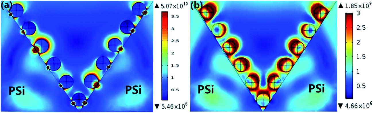 | ||
| Fig. 6 (a) The electric field distribution of the AgNPs@PSi substrate. (b) The electric field distribution of the MoS2@AgNPs@PSi substrate. | ||
In order to investigate the effect of different annealing temperatures on the AgNPs, we also prepared AgNPs@PSi at 400 °C, 600 °C and 700 °C, respectively. As shown in Fig. 7(a), some of the larger particles are distributed in the surface and valleys of PSi for an annealing temperature at 400 °C. The inset histograms shows the average size of AgNPs is about 47 nm. As illustrated in Fig. 7(c), compare with the AgNPs@PSi substrate for an annealing temperature at 500 °C, we can clearly see that the interparticle distance of AgNPs becomes larger and the density of AgNPs becomes smaller at 600 °C. The reason for this phenomenon may be that the high temperature to speed up the mobility of silver molecules, a part of the silver molecules with argon left the PSi surface. From the inset in Fig. 7(c), the average size of AgNPs is about 34 nm. When the temperature rises to 700 °C, most of the silver is evaporated and the interparticle distance becomes much larger, as shown in Fig. 7(d). We can see some bubbles around the particles. Which may be the PSi can not resistant to high temperature resulting in a slight melting of the PSi. The average size of AgNPs is about 24 nm according to the inset in Fig. 7(d). Raman spectra of 10−6 M R6G molecules on the AgNPs@PSi substrate for an annealing temperature at 400 °C, 500 °C, 600 °C and 700 °C was measured, respectively. As shown in Fig. 7(e), when the annealing temperature is 500 °C, the Raman enhancement effect of the AgNPs@PSi substrate is the best. The electric field of the AgNPs@PSi substrate at 400 °C, 600 °C and 700 °C were also simulated. According to Fig. 7(f)–(h), the EF of annealing temperature at 400 °C, 600 °C and 700 °C calculated is 4.49 × 10¹¹, 4.51 × 10¹⁰ and 2.11 × 10¹⁰, respectively. The results of these simulations also prove that the Raman enhancement effect of the AgNPs@PSi substrate is the best when the annealing temperature at 500 °C.
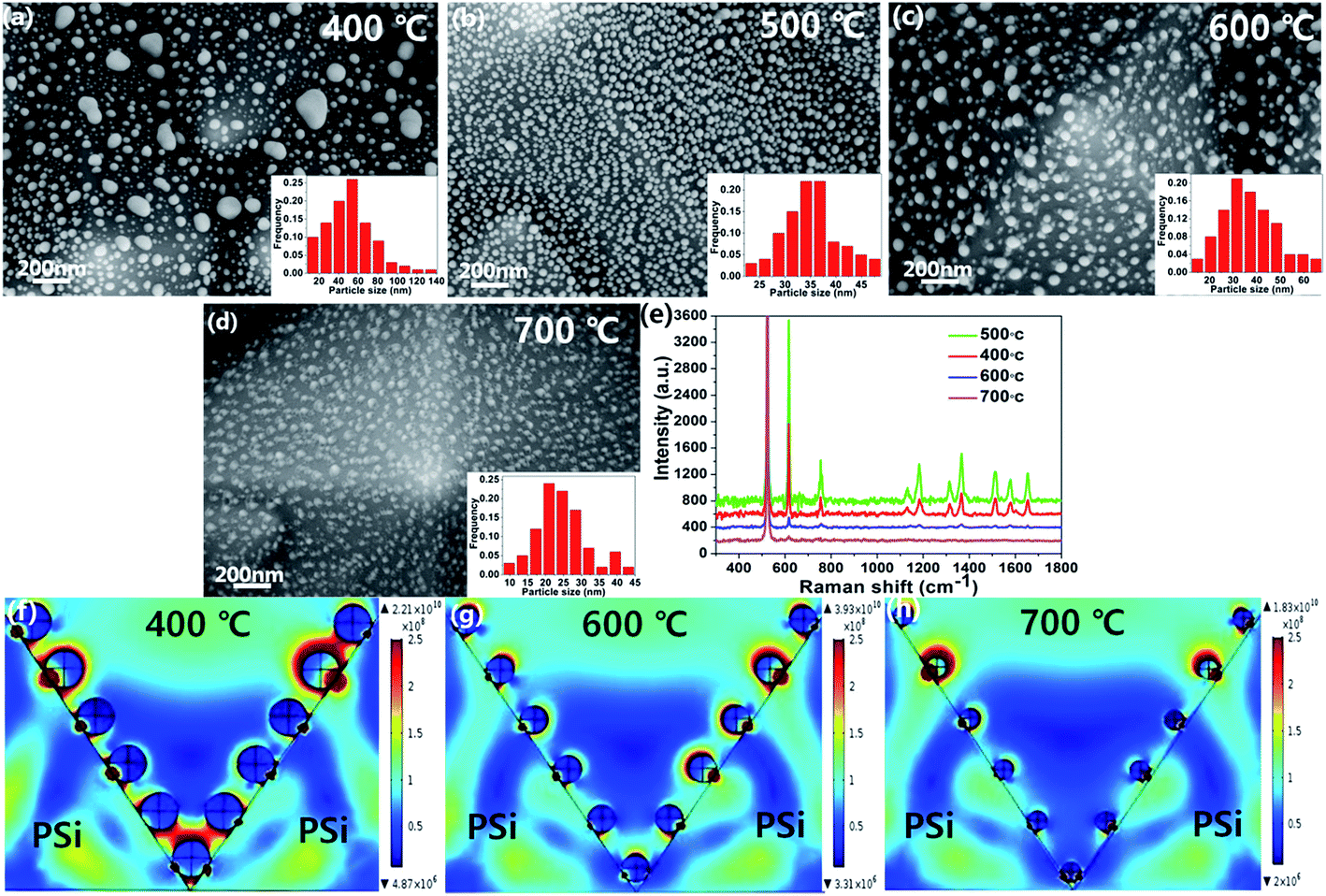 | ||
| Fig. 7 (a), (b), (c) and (d) are SEM image and histograms of particle size distribution of the AgNPs for an annealing temperature at 400 °C, 500 °C, 600 °C and 700 °C, respectively. (e) Raman spectra of R6G molecules that the concentration is 10−6 M on the AgNPs@PSi substrate with different annealing temperature from 400 °C to 700 °C. (f), (g) and (h) are the electric field distribution of the AgNPs@PSi substrate at 400 °C, 600 °C and 700 °C, respectively. | ||
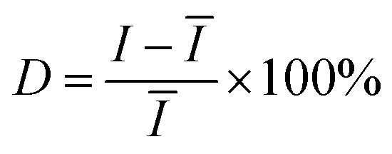
In addition to the high enhancement activity of SERS signals from the MoS2@AgNPs@PSi substrate, the hybrid system also shows many other excellent properties. Fig. 8(a) shows the SERS spectra of R6G molecules with concentration of 10−6 M from 20 positions on a same MoS2@AgNPs@PSi substrate. These SERS spectrum overlap to form a green shaded area. The black curve in the green shaded area is the average spectrum of the 20 SERS spectra. The perfect overlap of Raman spectra from these positions leads to a quite narrow green shaded area, which indicates the excellent similarity of the 20 SERS spectra. Fig. 8(b) shows the intensity distribution for the peak at 612 cm−1 of the R6G molecules with 10−6 M from 20 spectra on a same MoS2@AgNPs@PSi substrate. The shadow area represents the vibration range of the peak at 612 cm−1. The black line in the shaded area is the average intensity. The maximum intensity deviation of the SERS spectra is given by the formula:41
 | (2) |
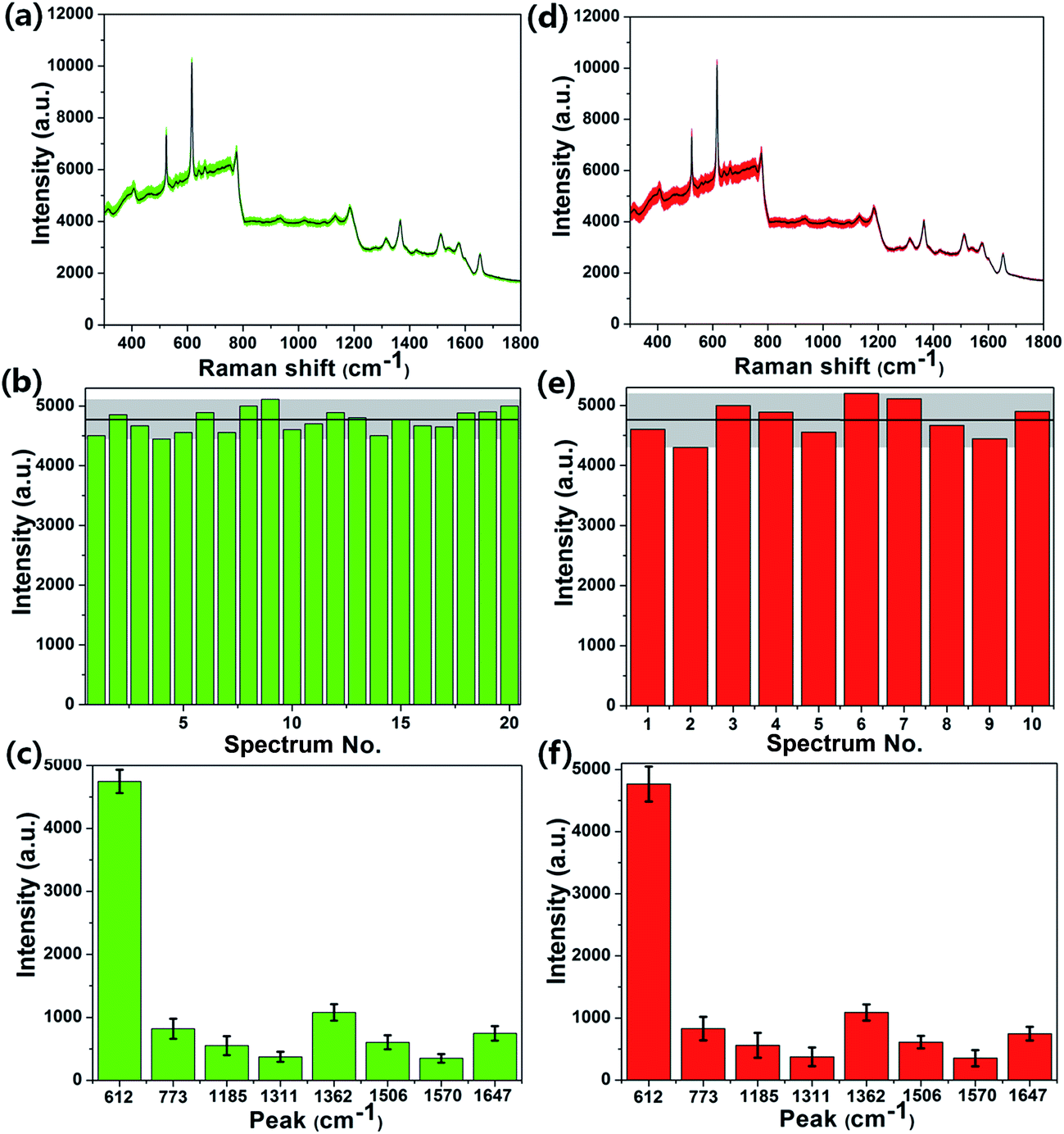 | ||
| Fig. 8 (a) Average Raman spectra (black line) of the R6G molecules with concentration of 10−6 M from 20 positions on a same MoS2@AgNPs@PSi substrate. (b) Intensity distribution for the peak at 612 cm−1 of the 20 Raman spectra. (c) Average intensity of characteristic peaks of the R6G molecules from the 20 Raman spectra. Error bars show the standard deviations. (d) Average Raman spectrum (black line) of the R6G molecules with concentration of 10−6 M from 10 MoS2@AgNPs@PSi substrates in different batches. (e) Intensity distribution for the peak at 612 cm−1 of the 10 spectra from 10 MoS2@AgNPs@PSi substrates in different batches. (f) Average intensity of characteristic peaks of the R6G molecules from the 10 spectra. Error bars show the standard deviations. | ||
As shown in Fig. 9(a), original SERS spectra of R6G molecules that the concentration is 10−6 M were collected from five randomly selected spots on the AgNPs@PSi substrate and the MoS2@AgNPs@PSi substrate, respectively. Obviously, background fluorescence of the MoS2@AgNPs@PSi substrate was significantly decreased compare with the AgNPs@PSi substrate, this phenomenon can be explained by the fluorescence quenching effect of MoS2. The characteristic of MoS2 can contribute to the uniformity of SERS signals from the MoS2@AgNPs@PSi substrate. In order to further investigate the stability of the MoS2@AgNPs@PSi substrate, the R6G concentration of 10−6 M was selected to compare the stability of the AgNPs@PSi and the MoS2@AgNPs@PSi substrates. The Raman intensity was measured every five days under the room temperature. As shown in Fig. 9(b), the measured SERS intensity attenuation of the AgNPs@PSi substrate is very obvious with the increase of the number of days. But for the MoS2@AgNPs@PSi substrate, the attenuation of the Raman intensity is very weak, as shown in Fig. 9(c). We made a line chart to make the contrast even more clear (Fig. 9(d)). One month later, the average intensity of peak at 612 cm−1 obtained from the AgNPs@PSi substrate is decreased 53%. Uplifting, the average intensity of the MoS2@AgNPs@PSi substrate is dropped only 15%. Through this comparison we draw a preliminary conclusion that the MoS2 film can tightly wrap the AgNPs and isolate it from the outside environment, effectively protect AgNPs from oxidation and endow the MoS2@AgNPs@PSi substrate long-term stability.
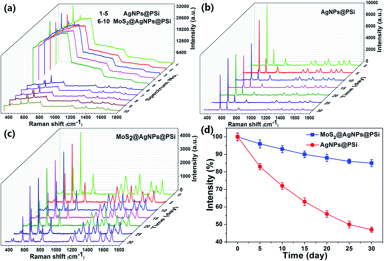 | ||
| Fig. 9 (a) Original Raman spectra of R6G molecules that the concentration is 10−6 M were collected from the AgNPs@PSi and MoS2@AgNPs@PSi substrates. (b) The Raman spectra of the AgNPs@PSi substrate was measured every five days under the room temperature. (c) The Raman spectra of the MoS2@AgNPs@PSi substrate was measured every five days under the room temperature. (d) The Raman intensity changes with time obtained from the AgNPs@PSi and MoS2@AgNPs@PSi substrates. | ||
4. Conclusions
In conclusion, by combining AgNPs, PSi and MoS2, a new SERS substrate has been presented based on MoS2@AgNPs@PSi. We using R6G as probe molecule, the SERS results indicate that the MoS2@AgNPs@PSi substrate has excellent sensitivity, uniformity, reproducibility and stability. The SERS behaviors of the AgNPs@PSi and MoS2@AgNPs@PSi substrates obtained in experiment were confirmed by theoretical calculations with the assist of a commercial COMSOL software. These experimental and theoretical results imply that the MoS2@AgNPs@PSi is expected to be an effective substrate for label-free SERS detections.Acknowledgements
The authors are grateful for financial support from the National Natural Science Foundation of China (11674199, 11604040, 11474187 and 11404193), Shandong Province Natural Science Foundation (ZR2014FQ032 and ZR2013HQ064), Excellent Young Scholars Research Fund of Shandong Normal University.References
- A. Barhoumi and J. N. Halas, J. Am. Chem. Soc., 2010, 132, 12792–12793 CrossRef CAS PubMed.
- K. Lee, V. P. Drachev and J. Irudayaraj, ACS Nano, 2011, 5, 2109–2117 CrossRef CAS PubMed.
- G. B. Jung, Y. M. Bae, Y. J. Lee, S. H. Ryu and H. K. Park, Appl. Surf. Sci., 2013, 282, 161–164 CrossRef CAS.
- X. M. Qian and S. M. Nie, Chem. Soc. Rev., 2008, 37, 912–920 RSC.
- J. Jiang, K. Bosnick, M. Maillard and L. Brus, J. Phys. Chem. B, 2003, 107, 9964–9972 CrossRef CAS.
- W. Li, P. H. C. Camargo, X. Lu and Y. Xia, Nano Lett., 2009, 9, 485–490 CrossRef CAS PubMed.
- D. Graham, D. G. Thompson, W. E. Smith and K. Faulds, Nat. Nanotechnol., 2008, 3, 548–551 CrossRef CAS PubMed.
- S. J. Lee, A. R. Morrill and M. Moskovits, J. Am. Chem. Soc., 2006, 128, 2200–2201 CrossRef CAS PubMed.
- X. Liu, J. Wang, Y. Wu, T. Fan, Y. Xu, L. Tang and Y. Ying, Sci. Rep., 2015, 5, 17167 CrossRef CAS PubMed.
- R. A. Tripp, R. A. Dluhy and Y. Zhao, Nanotoday, 2008, 3, 31–37 CrossRef CAS.
- Y. Sun, K. Liu, X. Hong, M. Chen, J. Kim, S. Shi, J. Wu, A. Zett and F. Wang, Nano Lett., 2014, 14, 5329–5334 CrossRef CAS PubMed.
- D. Zhang, Y. C. Wu, M. Yang, X. Liu, C. Ó. Coileáin, H. Xu, M. Abid, M. Abid, J. J. Wang, I. V. Shvets, H. Liu, Z. Wang, H. Yin, H. Liu, B. S. Chun, X. Zhang and H. C. Wu, RSC Adv., 2016, 6, 99053–99059 RSC.
- D. Zhang, Y. C. Wu, M. Yang, X. Liu, C. Ó. Coileáin, M. Abid, M. Abid, J. J. Wang, I. Shvets, H. Xu, B. S. Chun, H. Liu and H. C. Wu, Sci. Rep., 2016, 6, 30320 CrossRef CAS PubMed.
- Y. Deng, M. Chen, J. Zhang, Z. Wang, W. Huang, Y. Zhao, J. P. Nshimiyimana, X. Hu, X. Chi, G. Hou, X. Zhang, Y. Guo and L. Sun, Nano Res., 2016, 9, 1682–1688 CrossRef CAS.
- S. Su, H. Sun, W. Cao, J. Chao, H. Peng, X. Zuo, L. Yuwen, C. Fan and L. Wang, ACS Appl. Mater. Interfaces, 2016, 8, 6826–6833 CAS.
- J. Zhao, Z. Zhang, S. Yang, H. Zheng and Y. Li, J. Alloys Compd., 2013, 559, 87–91 CrossRef CAS.
- S. S. Singha, D. Nandi and A. Singha, RSC Adv., 2015, 5, 24188–24193 RSC.
- Z. Li, S. Jiang, Y. Huo, M. Liu, C. Yang, C. Zhang, X. Liu, Y. Sheng, C. Li and B. Man, Opt. Express, 2016, 24, 26097–26108 CrossRef PubMed.
- P. X. Chen, H. W. Qiu, S. C. Xu, X. Y. Liu, Z. Li, L. T. Hu, C. H. Li, J. Guo, S. Z. Jiang and Y. Y. Huo, Appl. Surf. Sci., 2016, 375, 207–214 CrossRef CAS.
- S. Xu, B. Man, S. Jiang, J. Wang, J. Wei, S. Xu, H. Liu, S. Gao, H. Liu, Z. Li, H. Li and H. Qiu, ACS Appl. Mater. Interfaces, 2015, 7, 10977–10987 CAS.
- C. Zhang, M. Liu, B. Y. Man, S. Z. Jiang, C. Yang, C. S. Chen, D. J. Feng, D. Bi, F. Y. Liu, H. W. Qiu and J. X. Zhang, CrystEngComm, 2014, 16, 8941–8945 RSC.
- H. W. Qiu, S. C. Xu, P. X. Chen, S. S. Gao, Z. Li, C. Zhang, S. Z. Jiang, M. Liu, H. S. Li and D. J. Feng, Appl. Surf. Sci., 2015, 332, 614–619 CrossRef CAS.
- C. Zhang, B. Y. Man, C. Yang, S. Z. Jiang, M. Liu, C. S. Chen, S. C. Xu, X. G. Gao and Z. C. Sun, Sci. Adv. Mater., 2014, 6, 399–404 CrossRef CAS.
- S. Xu, S. Jiang, J. Wang, J. Wei, W. Yue and Y. Ma, Sens. Actuators, B, 2016, 222, 1175–1183 CrossRef CAS.
- F. Giorgis, E. Descrovi, A. Chiodoni, E. Froner, M. Scarpa, A. Venturello and F. Geobaldo, Appl. Surf. Sci., 2008, 254, 7494–7497 CrossRef CAS.
- A. Chiolerio, A. Virga, P. Pandolfi, P. Martino, P. Rivolo, F. Geobaldo and F. Giorgis, Nanoscale Res. Lett., 2012, 7, 1–7 CrossRef PubMed.
- Y. Q. Wang, S. Ma, Q. Q. Yang and X. J. Li, Appl. Surf. Sci., 2012, 258, 5881–5885 CrossRef CAS.
- B. Kiraly, S. Yang and T. J. Huang, Nanotechnology, 2013, 24, 245704 CrossRef PubMed.
- L. M. Chen and Y. N. Liu, CrystEngComm, 2011, 13, 6481–6487 RSC.
- J. Yang, J. B. Li, Q. H. Gong, J. H. Teng and M. H. Hong, Nanotechnology, 2014, 25, 465707 CrossRef CAS PubMed.
- K. Q. Peng, Y. J. Yan, S. P. Gao and J. Zhu, Adv. Mater., 2002, 14, 1164 CrossRef CAS.
- X. Sun, N. Wang and H. Li, Appl. Surf. Sci., 2013, 284, 549–555 CrossRef CAS.
- G. Seniutinas, G. Gervinskas, R. Verma, B. D. Gupta, F. Lapierre, P. R. Stoddart, F. Clark, S. L. McArthur and S. Juodkazis, Opt. Express, 2015, 23, 6763–6772 Search PubMed.
- C. Zhang, B. Y. Man, S. Z. Jiang, C. Yang, M. Liu, C. S. Chen, S. C. Xu, H. W. Qiu and Z. Li, Appl. Surf. Sci., 2015, 347, 668–672 CrossRef CAS.
- C. Zhang, S. Z. Jiang, Y. Y. Huo, A. H. Liu, S. C. Xu, X. Y. Liu, Z. C. Sun, Y. Y. Xu, Z. Li and B. Y. Man, Opt. Express, 2015, 23, 24811–24821 CrossRef CAS PubMed.
- G. Madras and B. J. Mccoy, J. Chem. Phys., 2003, 119, 1683–1693 CrossRef CAS.
- C. Lee, H. Yan, L. E. Brus, T. F. Heinz, J. Hone and S. Ryu, ACS Nano, 2010, 4, 2695–2700 CrossRef CAS PubMed.
- Y. Chen, G. Tian, K. Pan, C. Tian, J. Zhou, W. Zhou, Z. Ren and H. Fu, Dalton Trans., 2012, 41, 1020–1026 RSC.
- Y. K. Kim, S. W. Han and D. H. Min, ACS Appl. Mater. Interfaces, 2012, 4, 6545–6551 CAS.
- S. Xu, J. Wang, Y. Zou, H. Liu, G. Wang, X. Zhang, S. Jiang, Z. Li, D. Cao and R. Tang, RSC Adv., 2015, 5, 90457–90465 RSC.
- S. Xu, S. Jiang, G. Hu, J. Wei, L. Wang, J. Zhang and Q. Li, Laser Phys., 2015, 25, 115601 CrossRef.
Footnote |
| † Both authors contributed equally to this work. |
| This journal is © The Royal Society of Chemistry 2017 |