
In situ epitaxial growth of GdF3 on NaGdF4:Yb,Er nanoparticles†
Jiangfeng
Li
ab,
Yunling
Jia
b,
Yuejiao
Xu
b,
Hui
Yang
c,
Ling-dong
Sun
b,
Chun-hua
Yan
 b,
Li-jian
Bie
*a and
Jing
Ju
*b
b,
Li-jian
Bie
*a and
Jing
Ju
*b
aSchool of Materials Science and Engineering, Tianjin University of Technology, Tianjin 300384, China
bCollege of Chemistry and Molecular Engineering, Peking University, Beijing 100871, China. E-mail: jingju@pku.edu.cn
cCapital Medical University, Beijing 100069, China
First published on 25th October 2017
Abstract
NaGdF4 is a well-known up-conversion material with potential applications in lasers and biolabels and used to be known as a thermally stable material bearing harsh natural conditions. In this work, a TEM electron beam was found to be able to manipulate the morphology of cubic-NaGdF4, changing it from solid nanoparticles to porous materials with nano-sized vacancies by electron beam irradiation. Electron beams also induce a structure change from cubic-NaGdF4 to GdF3. By controlling the current density of the TEM electron beam, the in situ epitaxial growth behavior of GdF3 (020) was observed at the NaGdF4 (111) interface. Structural correlations between two compounds were discussed to understand the epitaxial growth with a large lattice mismatch. These findings suggest a TEM electron beam can be used not only as an imaging tool, but also as an alternative paradigm for manipulating matter.
Introduction
Nanocrystals involving the organization of atoms into a crystal have been attracting intense research interest in fields such as functional materials including semiconductors,1 catalysts,2 luminescent materials3 and biomimetic materials,4 and in the synthesis processes.5 The novel characteristics of these nanomaterials, and the resulting potential for applications, derive from the fact that their properties lie between those of molecules and crystalline solids. As the size of a particle increases from the angstrom to the nanometer and micrometer scale, fundamental changes occur.6 The molecular symmetry changes to a crystal lattice with periodic long-range order, discrete energy levels turn into a continuous band structure and electrons confined in the molecular orbitals become delocalized.Technically tracking crystal growth and clearly understanding the formation mechanism of nanoparticles are essentially important for designing and the synthesis of those functional nanomaterials. Thanks to continuous development in microscope instrumentation, especially in situ microscopy with aberration correctors,7,8 energy monochromator,9 ultra-fast recording cameras, special specimen chambers capable of injecting chemical gases,10 and a variety of specialty sample holders available (heating,11 cooling,12 straining,13 indenting,14 and electric pulsing15), pursuing the formation mechanism of nanocrystal growth on the nanometer or atomic scale is no longer a dream. On the other hand, the interactions of a beam of electrons from transmission electron microscopy (TEM) with materials have also been intensively investigated. Energy transfer during electron irradiation proceeds by two paths: electronic interactions and nuclear (knock-on) collisions.16,17 Although structurally detrimental, radiation damage is observed in some systems, such as Au nanoparticles,18 metal oxide nanoparticles,19 silicon oxide nanowires,20 and molecular sieve,21 the interaction offers opportunities for manipulation and even fabrication of interesting nanostructures.22,23
NaGdF4 exhibits an adequate thermal and environmental stability and hence has been reported as one of the most efficient infrared-to-visible up-conversion (UC) fluorescent host materials.24,25 For example, nano hexagonal-NaGdF4:Yb,Er is a well-known UC material with potential applications in lasers and biolabels.26 Although their structure, morphology and luminescent properties have been sufficiently investigated, there are very few reported instances of introducing localized order/crystallinity by an electron beam. Feng et al.27 reported hole-formation by electron beam irradiation and Sun et al.28 reported the remodeling of beta-NaGdF4:Yb,Er. These observations suggest that (S)TEM beams can, in principle, be used to achieve subnanometer level bulk nanofabrication and create complex nanostructures.
Herein, we report observations of the structural evolution, crystallographic conversion and in situ epitaxial growth of GdF3 on cubic NaGdF4:Yb,Er nanoparticles induced by TEM electron irradiation. The mechanisms of the structural evolutions of NaGdF4:Yb,Er nanocrystals are also discussed.
Experimental
The synthesis of NaGdF4:Yb,Er was carried out using standard oxygen-free procedures and commercially available reagents. Rare-earth oxides, oleic acid (OA; 90%, Alpha), oleylamine (OM; >80%, Acros), 1-octadecene (ODE; >90%, Acros), trifluoroacetic acid (99%, Acros), Na(CF3COO) (>97%, Acros), absolute ethanol, chloroform, hexane, and toluene were used as received. RE(CF3COO)3 and Na(CF3COO) were prepared by a literature method.29 A typical procedure25 is as follows: to a three-necked flask of 40 mmol OA/OM/ODE at room temperature were added given amounts of Na(CF3COO) and RE(CF3COO)3 (1 mmol). Then the slurry was heated to 100 °C to remove water and oxygen, with vigorous magnetic stirring under vacuum for 30 min in a temperature-controlled electromantle, and thus formed a transparent solution. The solution was then heated to a certain temperature in the range of 250–330 °C at a rate of 20 K min−1 and maintained at the given temperature for 15–45 min under an Ar atmosphere. When the reaction was completed, an excess amount of ethanol was poured into the solution at room temperature. The resultant mixture was centrifugally separated, and the products were collected. The as-precipitated nanocrystals were washed several times with ethanol and dried in air at 70 °C overnight. The yields of all the obtained nanocrystals without any size selection were 60–70%. All of these as-prepared nanocrystals could be easily re-dispersed in various organic solvents such as hexane, toluene, and chloroform.Instrumentation
Powder X-ray diffraction (XRD) patterns of the as-prepared products were recorded on a Rigaku D/MAX-2000 diffractometer (Japan) with a slit of 1/2° at a scanning rate of 2° min−1, using Cu Kα radiation (λ = 1.5406 Å). For transmission electron microscopy (TEM) observations, nanocrystals were dispersed in deionized water by ultrasonication and then dropped on ultrathin carbon film-coated copper grids. To decrease the contamination effect, the deposited copper grid was washed by a plasma cleaner using an IBSS Gentle Asher Chamber Model A01 in air flow of 10 to 20 watt in power and with individual washing times of 10 min. High-resolution TEM (HRTEM) characterization was performed with a JEM-2100F FEG-TEM operated at 200 kV with a current density of 20–52 pA cm−2.Results
Fig. S1† gives the XRD pattern of NaGdF4:Yb,Er, showing a pure cubic-NaGdF4 structure, consistent with Joint Committee on Powder Diffraction Standard (JCPDS) card number: 27-0697. Fig. 1(a) shows a large area TEM image of nearly monodispersed NaGdF4:Yb,Er with a very low degree of agglomeration. To avoid irradiation effects during imaging, all the images in this work were taken within 3 s, including the camera exposure period and objective focus adjustments. The nanoparticles present a normal contrast of solid particles upon quick imaging. Most spheres are found to be 20 ± 5 nm in diameter but a small number are less than 10 nm. Fig. 1(b) shows the HRTEM image of a single nanoparticle. The image shows a perfect cubic symmetry of the cubic-phase. The corresponding FFT pattern in Fig. 1(c) indicates that the particle singly crystalline. The assigned planes from the FFT pattern are {220} plane groups with d = 1.99 Å and the zone axis is [111]. These data coincide with the crystallographic ones of cubic-NaGdF4 with an Fm3m space group (JCPDS card number: 27-0697).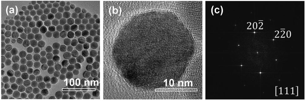 | ||
| Fig. 1 TEM images of NaGdF4:Yb,Er nanoparticles. (a) A large area exhibiting nearly monodispersed particles. (b) The HRTEM image of a single nanoparticle and (c) its corresponding FFT pattern. | ||
A prolonged irradiation time (t) with a current density of 52 pA cm−2 at 200 kV leads to vacancies occurring in the NaGdF4:Yb,Er particles (Fig. 2). The vacancies are several nanometers in size. With increasing irradiation time, more vacancies appear and tend to coalesce and grow into larger ones. On the other hand, monodispersed nanoparticles shrink and agglomerate. One single particle was selected at an exposure time of 21 min and 61 min respectively to do the HRTEM analysis, as shown in Fig. 3. At t = 21 min, the particle possesses a cubic-phase structure (Fig. 3(a)), its FFT analysis (Fig. 3(c)) shows (−111) and (220) reflections at right angles and with d = 3.20 and 1.99 Å, respectively. At t = 61 min, the particle does not change its morphology much, but exhibits a GdF3 structure (Fig. 3(b)). FFT analysis for the HRTEM image in Fig. 3(b) gives GdF3 (0−11) and (111) reflections with an angle of 68° and with d = 3.80 and 3.30 Å, respectively. Energy dispersive X-ray spectroscopy (EDS) was performed to investigate the composition change of the area in Fig. 2 at individual exposure times. By assuming that the ejection of the Yb atom by the electron beam was minimal as it is the heaviest element in the particle, the atomic ratios of the rest of the elements were normalized with reference to Yb and are listed in Table 1. The Er content in the particle is negligible and hence not listed in the table. The results reveal that the contents of Na and F, measured with the beam being exposed on the particles with time, decrease continuously, whereas the contents of Gd keep almost constant. According to the normalized data, Na and F atoms are heavily lost during electron beam irradiation, strongly indicating that light elements, such as Na and F, were knocked out of the crystal by electron beam irradiation. Note that each EDS measurement was acquired for 1 minute, and the irradiation intensity was controlled at less than 8 pA cm−2 to slow down the structural alteration of the particles, so the EDS analyses do not affect the structural alteration process much.
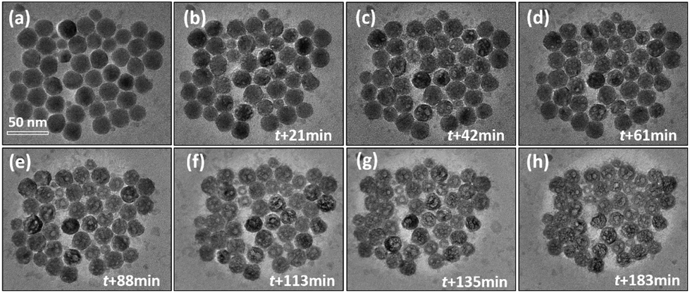 | ||
| Fig. 2 (a–h) Time dependence of the morphology reconfiguration of NaGdF4:Yb,Er nanoparticles induced by 200 kV electron beam irradiation with the current density at 52 pA cm−2. The scale bar is 50 nm for all. | ||
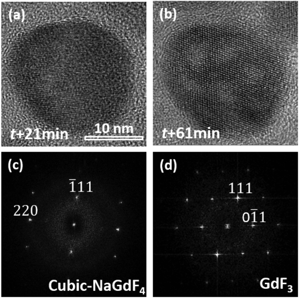 | ||
| Fig. 3 TEM images of an individual NaGdF4:Yb,Er nanoparticle after electron beam irradiation for (a) 21 min and (b) 61 min with the current density at 52 pA cm−2, (c) and (d) show their corresponding FFT patterns labeled with Miller indices. | ||
| Time (min) | Yb | Na | Gd | F |
|---|---|---|---|---|
| 0 | 1 | 2.5 | 4.25 | 19.5 |
| 21 | 1 | 2 | 4.4 | 18.2 |
| 42 | 1 | 1.67 | 4.33 | 16.3 |
| 61 | 1 | 1.67 | 4.33 | 12.8 |
| 88 | 1 | 1.67 | 4.5 | 12 |
| 113 | 1 | 1.43 | 4.43 | 11.57 |
| 183 | 1 | 1.25 | 4.125 | 10.25 |
To further study the phase transition process that happened on cubic-NaGdF4:Yb,Er and the detailed crystal growth of GdF3, a focused electron beam was employed to scatter on a small area, including two adjacent particles as shown in Fig. 4. The intensity of the beam is controlled at 40 pA cm−2 to slow down and acquire precisely the crystal growth detail. At first, two adjacent particles exhibit cubic-NaGdF4:Yb,Er single crystalline structures with (111) planes of 3.17 Å, and the two particles have a clear boundary as shown in Fig. 4(a) and Fig. S2.† Since the d-spacings for GdF3 (111) (d111 = 3.24 Å) and (020) (d020 = 3.49 Å) are close to those of cubic-NaGdF4 (111), image profile analyses for the individual HRTEM images in Fig. 4 were executed for accuracy and the results are listed in Fig. S2–S7.† Both particles show cubic-NaGdF4 (111) planes with a plane distance of 3.172 Å for the left and of 3.174 Å for the right particle, which are consistent with the JCPDS card.
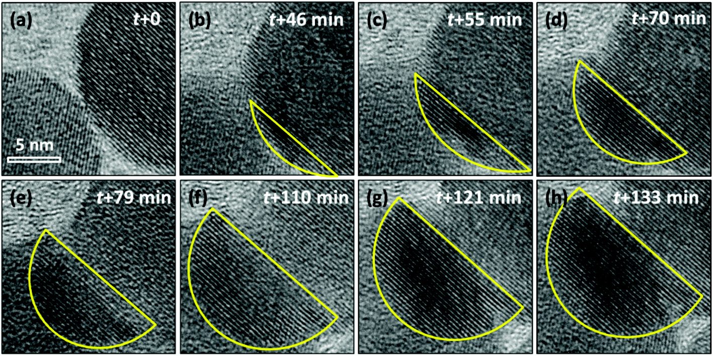 | ||
| Fig. 4 (a–h) Time dependence of the in situ epitaxial growth of GdF3 on NaGdF4 at the interface induced by a focused electron beam with a current density of 40 pA cm−2. The scale bar in all figures is 5 nm. GdF3 layers are marked with yellow lines for a guide to the eye. | ||
When the beam irradiation was kept for 46 min, two particles were observed to merge at the interface where an obvious contrast change appears (Fig. 4(b)). The new area with a dark contrast is indicated as yellow line to guide the eye. The HRTEM images were analyzed to provide additional insight on the microstructure of the interface. As shown in Fig. 5(a), the orange arrow shows the crystalline fringes at the interface of the two particles. The image profile shown in Fig. 5(b) illustrates that the d-spacings of the first four crystalline fringes are 3.43 Å, 3.65 Å and 3.53 Å, respectively. Compared to the NaGdF4 (111) plane of 3.17 Å, an 11.5% expansion on average was observed. This expansion has not been well documented in previous studies of NaGdF4:Yb,Er made by similar synthetic approaches. This expansion only occurs within 1.4 nm of the NaGdF4:Yb,Er interface, and then gradually decreases and completely disappears 2.3 nm away from the interface where the spacing approaches a constant bulk value of 3.17 Å (Fig. 5(c)). The d-spacings of 3.43 Å, 3.65 Å and 3.53 Å can be attributed to either (020) or (101) of GdF3 (Pnma, JCPDS: 49-1804). Combined with the EDS results mentioned above, Na and F atoms were kicked out from the NaGdF4 phase. Hence, the GdF3 component of the heterostructure is observed at the interface.
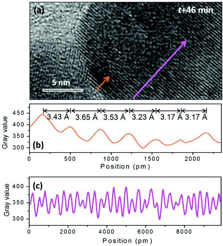 | ||
| Fig. 5 (a) HRTEM image of the GdF3–NaGdF4 interface at the irradiation time of 46 min. (b) and (c) Profiles of line scans along the GdF3–NaGdF4 interface (orange arrow) and along the particle body of NaGdF4 (111) (pink arrow). | ||
At t = 55 min in Fig. 4(c) and Fig. S3,† two particles merge further, in total 7 atomic layers with a d-spacing of 3.41 Å on average were observed at the interface, different from that of 3.17 Å in the body of the cubic-NaGdF4 particle. The d-spacing of 3.41 Å is indexed to (020) of GdF3. Interestingly, the (020) GdF3 planes are parallel to the (111) plane of cubic-NaGdF4, even though some contrast was lost in the bulk cubic-NaGdF4 particle due to the existence of vacancies. These findings were further verified by the case of 70 min in Fig. 4(d) and Fig. S4;† 12 layers of (020) of GdF3 with d-spacing of 3.48 Å grew next to the (111) plane of cubic-NaGdF4 with a d-spacing of 3.186 Å. Obviously, this is an epitaxial growth happening on the interface of the (111) plane of cubic-NaGdF4.
GdF3 keeps growing with time, and its growth direction is along GdF3 (020), which is parallel to the NaGdF4 (111) substrate. When the observation was terminated at t = 133 min, a total of 25 atomic layers of GdF3 (020) had grown. In Fig. 6(a), a clear crystal interface between GdF3 and NaGdF4 is observed as indicated by a white dashed line. A line profile was carried out along the growth direction as indicated in Fig. 6(a), and the result is shown in Fig. 6(c). The averaged d-spacing for GdF3 is 3.46 Å and that for NaGdF4 is 3.17 Å. FFT analysis of the area in Fig. 6(b) shows the co-existence of (111) of NaGdF4 and (020) of GdF3 with same direction. The d-spacings for GdF3 (020) and NaGdF4 (111) are 3.463 Å and 3.172 Å, respectively, which are consistent with the profile analyses and give clear evidence of the epitaxial growth of GdF3 on NaGdF4.
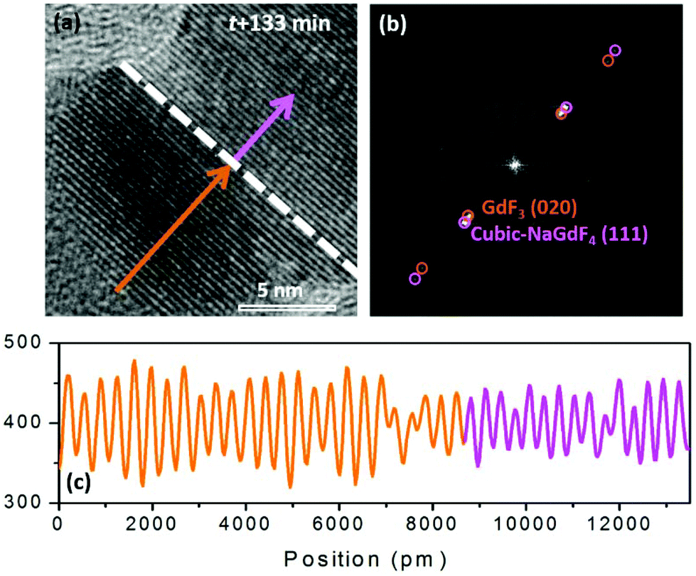 | ||
| Fig. 6 (a) At t = 133 min, the HRTEM image shows a clear crystal interface between GdF3 and NaGdF4 indicated by a white dash line. (b) The associated FFT analysis definitely shows the co-existence of (111) of NaGdF4 and (020) of GdF3 with same direction. (c) Line scan indicated by the orange arrow and the pink arrow in (a) shows the averaged d-spacing for GdF3 is 3.46 Å and that for NaGdF4 is 3.17 Å, corresponding to the GdF3 (020) plane and NaGdF4 (111) plane. | ||
These findings suggest that electron beam can be used not only as an imaging tool, but also as an alternative paradigm for manipulating matter. E-beam lithography in scanning electron microscope (SEM) geometry is used to fabricate 3D structures at the nanometer scale.30 However, due to the finite interaction volume for lower-energy electron beams, manipulating at the atomic scale is not feasible and the typical minimal feature size only recently reached the sub-10 nm regime. Hence, of interest is nanofabrication using highly energetic (scanning) transmission electron microscope ((S)TEM) beams, that have over last several decades evolved to power atomic resolution imaging tools and also offer the advantage of an atomically confined interaction volume.31 It is well known that (S)TEM beams can induce hole formation in the specimens via knock-on damage.27 This effect can also be used to form nanoscale patterns in thin amorphous films32 as well as single- and few-layer graphene.33
The interaction of the electron beam with material can give rise to phenomena on multiple energy scales, ranging from high-energy electron-atom collisions at primary beam energies ultimately to thermalization and local heating. The heat generation was assumed to occur due to inelastic collisions of electrons of the electron beam with the electrons in the sample.16 To estimate the increase of the temperature along the electron beam path in the sample, we apply an empirical calculation for a thin foil specimen according to Egerton34 and the maximum ΔT is no higher than 33.5 K. This temperature increase is much lower than the decomposition temperature of cubic-NaGdF4. Based on this observation, we conclude that thermal effects cannot account for the experimentally observed behaviors; therefore, the observed phenomena are likely knock-on in origin. Knock-on collisions involve the interaction of the incident electron with an atom's nucleus. If the transferred energy is greater than the displacement threshold energy, the atom can be displaced to become interstitial or be ejected out.
A focused electron beam can also be considered a beam-assisted chemical vapor deposition (CVD) technique. But, in this case, the energy required to dissociate the precursor molecules is not thermally provided, as occurs in CVD, but by electron beam irradiation, whilst the substrate is generally maintained at room temperature.
The conventional CVD method is widely used to obtain low-dimensional materials, such as graphene35 and CNT.36 CVD is known to involve the decomposition of a carbon feedstock, with the aid of heat and metal catalysts. Graphene is grown on the surface of metal catalysts in an epitaxial way. Surface orientation affects the quality of the graphene produced. Ishihara et al.37 and Wood et al.38 grew graphene on a polycrystalline Cu with several surface orientations of (111), (101) and (100). Single-layer graphene or few-layer graphene was preferentially formed on the Cu (111) surface than on Cu the (100) surface as a result of the good lattice matching between Cu (111) and graphene nucleated on such nuclei.
In this work, the interactions between the energetic electrons with atoms’ nuclei from cubic-NaGdF4 feedstock lead to the decomposition of cubic-NaGdF4. These interactions can be treated as an elastic two-body collision. On the other hand, these atoms are bonded in the crystal field. According to elastic collision theory16 and crystal field theory,39 light atoms, such as Na and F, are much more easily ejected out of the solid sample and purged by the vacuum system. The remaining vaporized atoms are mainly the heavy atoms Gd and Yb. Since the content of F is much higher than that of the other elements, F atoms together with heavy elements condense again into a solid when they deposit at the interface of two particles. Therefore, cubic-NaGdF4 undergoes a solid–gas-solid process, similar to the CVD process.
In epitaxial growth of lattice mismatched materials, the shell lattice adapts to the underlying core lattice structure, resulting in a substantial lattice strain in the epitaxial layer (shell). The strain in the epitaxial layer beyond a critical thickness (about 1–2 monolayers) relaxes, leading to shape inhomogeneity and anisotropic structures. Critical for growing thick shells, it is generally accepted that the lattice mismatch between the core and the shell should be minimal (<2%).40 The d-spacings for cubic-NaGdF4 (111) and GdF3 (020) are 3.17 Å and 3.49 Å, respectively, and the lattice mismatch is greater than 10%. A large lattice mismatch was reported in some systems like the Cd/Zn chalcogen core–shell structure with a 12% lattice mismatch41 and the Ge/Si multilayer structure with a 4.2% lattice mismatch.42 Considering the two structures in this work may give some hints as to the growth. Cubic-NaGdF4 adopts a face-centered symmetry with the stacking pattern of a (111) plane, shown in Fig. 7(a). Gd/Na atoms locate in the (111) plane, surrounded by six F atoms near the plane. Three F atoms are above the (111) plane and the other three beneath it. In total, eight F atoms are bonded with Gd/Na atoms, with the two from the two neighboring Gd/Na layers. GdF3 adopts an orthorhombic symmetry with the stacking pattern of a (020) plane, as shown in Fig. 7(b). In the (020) plane, Gd atoms are bonded with three F atoms with isotropic positions. The other F atomic site locates between the (020) plane, and six F atoms are bonded with one Gd atom. Totally nine F atoms are bonded with the Gd atoms in GdF3. Although the coordination details differ between the two materials, the stacking patterns are quite similar. The Gd/Na atomic layers in both are linked by two F atomic layers in between. The nearest distance of two F atoms from the two F layers is 2.7350 Å for cubic-NaGdF4 and 2.6015 Å for GdF3. We know epitaxial growth strongly depends on the atomic stacking pattern along the growth direction, so such a linkage similarity may give some hint to explain the in situ epitaxial growth of GdF3 (020) on cubic-NaGdF4 (111). Considering the similarity of the crystal fringe, GdF3 (111) is the closest one to NaGdF4 (111). However, atomic linkages shown in Fig. S8† tell us that Gd atoms do not totally locate in the (111) plane and the linkage modes of Gd and F atoms are quite different from that in Fig. 7(a). From the structural point of view, the GdF3 (020) plane is facile to grow on the NaGdF4 (111) plane, although the lattice mismatch is larger than that of the GdF3 (111) plane.
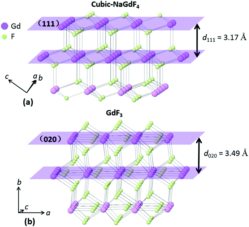 | ||
| Fig. 7 Crystal structure for (a) cubic-NaGdF4 adopting a face-centered symmetry with the stacking pattern of a (111) plane and for (b) GdF3 adopting an orthorhombic symmetry with a stacking pattern of a (020) plane. Gd/Na atoms are indicated as purple spheres and F atoms as green ones. | ||
Conclusions
In summary, an energetic TEM electron beam was employed to manipulate the cubic-NaGdF4 morphology from a solid nano-particle to a porous material with nano-sized vacancies; from the structural point of view, the electron beam induced a structural transformation from cubic-NaGdF4 to orthorhombic GdF3; from the nanocrystal growth viewpoint, the electron beam induced the in situ epitaxial growth of GdF3 (020) on the cubic-NaGdF4 (111) plane. The novelty points in this work are that a traditionally thermally stable phase, like NaGdF4 luminescent materials, can be patterned on the nanoscale and a conventional 3D material can be manipulated as a 2D material with only several atomic layers, realized by in situ electron irradiation. It is helpful for us to understand an old material with new dimensions.Conflicts of interest
There are no conflicts to declare.Acknowledgements
The authors gratefully acknowledge a valuable discussion with Prof. Fangtian You. We appreciate the assistance of Hao Dong and Xiaoyong Wang in the sample synthesis. This work was supported by the National Natural Science Foundation of China (Grant No. 21271139 and 21201012).Notes and references
- M. Nirmal and L. Brus, Acc. Chem. Res., 1999, 32, 407 CrossRef CAS.
- Z. Y. Zhou, N. Tian, J. T. Li, I. Broadwell and S. G. Sun, Chem. Soc. Rev., 2011, 40, 4167 RSC.
- Y. S. Liu, D. T. Tu, H. M. Zhu, R. F. Li, W. Q. Luo and X. Y. Chen, Adv. Mater., 2010, 22, 3266 CrossRef CAS PubMed.
- H. R. Luckarift, J. C. Spain, R. R. Naik and M. O. Stone, Nat. Biotechnol., 2004, 22, 211 CrossRef CAS PubMed.
- N. D. Loh, S. Sen, M. Bosman, S. F. Tan, J. Zhong, C. A. Nijhuis, P. Král, P. Matsudaira and U. Mirsaidov, Nat. Chem., 2017, 9, 77 CAS.
- D. H. Jara, S. J. Yoon, K. G. Stamplecoskie and P. V. Kamat, Chem. Mater., 2014, 26, 7221 CrossRef CAS.
- B. Freitag, S. Kujawa, P. M. Mul, J. Ringnalda and P. C. Tiemeijer, Ultramicroscopy, 2005, 102, 209 CrossRef CAS PubMed.
- S. Takedan, Y. Kuwauchi and H. Yoshida, Ultramicroscopy, 2015, 151, 178 CrossRef PubMed.
- P. C. Tiemeijer, M. Bischoff, B. Freitag and C. Kisielowski, Ultramicroscopy, 2012, 114, 72 CrossRef CAS PubMed.
- T. Yokosawa, T. Alan, G. Pandraud, B. Dam and H. Zandbergen, Ultramicroscopy, 2012, 112, 47 CrossRef CAS PubMed.
- Y. M. Lei, J. Sun, H. W. Liu, X. Cheng, F. Chen and Z. W. Liu, Chem. – Eur. J., 2014, 20, 11313 CrossRef CAS PubMed.
- M. D. Graef, M. A. Willard, M. E. Mchenry and Y. Zhu, IEEE Trans. Magn., 2001, 37, 2663 CrossRef.
- A. Kröger, S. Dziaszyka, J. Frenzela, C. Somsena, A. Dlouhy and G. Eggelera, Mater. Sci. Eng., A, 2008, 481, 452 CrossRef.
- J. T. M. De Hosson, W. A. Soer, A. M. Minor, Z. W. Shan, E. A. Stach, S. A. S. Asif and O. L. Warren, J. Mater. Sci., 2006, 41, 7704 CrossRef.
- P. M. F. J. Costa, D. Golberg, M. Mitome, S. Hampel, A. Leonhardt, B. Buchner and Y. Bando, Nano Lett., 2008, 8, 3120 CrossRef CAS PubMed.
- F. Seitz and J. S. Koehler, Solid State Physics, 1956, vol. 2, p. 305 Search PubMed.
- W. A. Mckinley and H. Feshbach, Phys. Rev., 1948, 74, 1759 CrossRef CAS.
- M. José-Yacamán, C. Gutierrez-Wing, M. Miki, D. Q. Yang, K. N. Piyakis and E. Sacher, J. Phys. Chem. B, 2005, 109, 9703 CrossRef PubMed.
- A. H. Latham, M. J. Wilson, P. Schiffer and M. E. Williams, J. Am. Chem. Soc., 2006, 128, 12632 CrossRef CAS PubMed.
- X. F. Zhu, J. B. Su, Y. Wu, L. Z. Wang and Z. G. Wang, Nanoscale, 2014, 6, 1499 RSC.
- R. Csencsits and R. Gronsky, Ultramicroscopy, 1987, 23, 421 CrossRef CAS.
- A. V. Krasheninnikov and F. Banhart, Nat. Mater., 2007, 6, 723 CrossRef CAS PubMed.
- S. J. Wu, F. Cao, H. Zheng, H. P. Sheng, C. Liu, Y. Liu, D. S. Zhao and J. B. Wang, Appl. Phys. Lett., 2013, 103, 243101 CrossRef.
- S. Heer, K. Kömpe, H.-U. Güdel and M. Haase, Adv. Mater., 2004, 16, 2102 CrossRef CAS.
- H. X. Mai, Y. W. Zhang, R. Si, Z. G. Yan, L. D. Sun, L. P. You and C. H. Yan, J. Am. Chem. Soc., 2006, 128, 6426 CrossRef CAS PubMed.
- L. Q. Xiong, Z. G. Chen, M. X. Yu, F. Y. Li, C. Liu and C. H. Huang, Biomaterials, 2009, 30, 5592 CrossRef CAS PubMed.
- W. Feng, L. D. Sun, Y. W. Zhang and C. H. Yan, Small, 2009, 5, 2057 CrossRef CAS PubMed.
- X. Y. Sun, B. R. Wang, I. Kempson, C. Y. Liu, Y. Hou and M. Y. Gao, Small, 2014, 10, 4711 CrossRef CAS PubMed.
- J. E. Roberts, J. Am. Chem. Soc., 1961, 83, 1087 CrossRef CAS.
- L. Wang, S. Zhang, Q. P. Wang, J. Q. Chen, W. Jiang and R. T. Chen, Appl. Phys. A, 2009, 95, 329 CrossRef CAS.
- S. Zaefferer, Cryst. Res. Technol., 2011, 46, 607 CrossRef CAS.
- W. G. Stratton, J. Hamann, J. H. Perepezko and P. M. Voyles, Intermetallics, 2006, 14, 1061 CrossRef CAS.
- H. G. Duan, E. Q. Xie, L. Han and Z. Xu, Adv. Mater., 2008, 20, 3284 CrossRef CAS.
- R. F. Egerton, P. Li and M. Malac, Micron, 2004, 35, 399 CrossRef CAS PubMed.
- Y. Zhang, L. Zhang and C. Zhou, Acc. Chem. Res., 2013, 46, 2329 CrossRef CAS PubMed.
- M. F. L. De Volder, S. H. Tawfick, R. H. Baughman and A. J. Hart, Science, 2013, 339, 535 CrossRef CAS PubMed.
- M. Ishihara, Y. Koga, J. Kim, K. Tsugawa and M. Hasegawa, Mater. Lett., 2011, 65, 2864 CrossRef CAS.
- J. D. Wood, S. W. Schmucker, A. S. Lyons, E. Pop and J. W. Lyding, Nano Lett., 2011, 11, 4547 CrossRef CAS PubMed.
- L. Glasser and H. D. B. Jenkins, J. Am. Chem. Soc., 2000, 122, 632 CrossRef CAS.
- T. Watahiki, F. Grosse, W. Braun, V. M. Kaganer, A. Proessdorf, A. Trampert and H. Riechert, Appl. Phys. Lett., 2010, 97, 031911 CrossRef.
- A. M. Smith, A. M. Mohs and S. M. Nie, Nat. Nanotechnol., 2009, 4, 56 CrossRef CAS PubMed.
- J. Michel, J. F. Liu and L. C. Kimerling, Nat. Photonics., 2010, 4, 527 CrossRef CAS.
Footnote |
| † Electronic supplementary information (ESI) available: XRD pattern of the as-synthesized NaGdF4:Yb,Er and HRTEM images of the samples at individual irradiation time under TEM e-beam. The crystal structure of GdF3 from the (111) stacking direction. See DOI: 10.1039/c7qi00527j |
| This journal is © the Partner Organisations 2017 |