Excitonic quantum confinement modified optical conductivity of monolayer and few-layered MoS2†
Received
17th June 2016
, Accepted 26th August 2016
First published on 26th August 2016
Abstract
Optical conductivity plays an important role in characterizing the optoelectronic properties of two-dimensional materials. Here we derive the complex optical conductivities for monolayer and few-layered MoS2 films from their reflectance and transmittance responses. We show that the excitonic quantum confinement effect significantly modifies both the peak energy and magnitude of their optical conductivity, manifested by a gradual blueshift in energy (consistent with two well-known models for quantum well systems) and exponential attenuation in magnitude with decreasing layer number. More importantly, the C excition induced optical conductivity peak exhibits the strongest dependence on the MoS2 layer number because of its largest Bohr radius among the A, B and C excitons. This unambiguously confirms the strong influence of quantum confinement effect in the optical conductivity of MoS2, shedding important insights into understanding its rich exciton-related optical properties and therefore facilitating potential applications in optoelectronic devices.
Introduction
In recent years, two-dimensional (2D) transition metal dichalcogenide (TMDC) materials with the generalized formula MX2 (M = Mo, W; X = S, Se, and Te) have received burgeoning research interest due to their peculiar physicochemical properties.1–5 Their electronic states generally are subject to strong interlayer coupling and undergo transitions from the indirect bandgap in the bulk form to the direct bandgap in monolayers. In particular, the direct bandgap energy in many monolayer TMDCs lies in the visible and near infrared range, making them ideal candidates for 2D optoelectronic applications.1,2 Among various TMDCs, MoS2 is a widely-studied example, which consists of a sandwich structure of S–Mo–S in each layer.2 Few-layered MoS2 is an excellent light absorber, with the absorption spectrum generally composed of three characteristic peaks due to excitonic resonance and interband transitions.6 In addition, with the abundance of molybdenite in nature, MoS2 is chemically more stable and relatively cheaper than other TMDCs. Previous studies have proven that monolayer MoS2-based photodetectors and phototransistors exhibit high photo-responsivity and a large photo-thermoelectric effect.7,8 Few-layered MoS2 with thickness-dependent bandgap energy is also promising for fiber lasers, solar cells, optical lenses, gratings, etc.2,9–11 In all the aforementioned optoelectronic applications, the optical conductivity of MoS2 plays a key role in characterizing the electronic states of the system and links the current density to an externally applied electric field.12
In a typical 2D TMDC material, optical conductivity stems from interband transitions due to electron–photon interaction. When the material absorbs one photon, the generated electron and hole will propagate with the same velocity amplitude but opposite direction, resulting in the so called band nesting.13 In the nesting region of the band structure, the conduction and valence bands are parallel to each other in energy. The band nesting gives rise to a singularity in the joint density of states, producing a greatly enhanced optical conductivity.6,13 Recently, Wang et al. have successfully measured the photoexcited carrier lifetimes in monolayer and few-layered MoS2 flakes on the basis of frequency-dependent optical conductivity, without carrying out a systematic analysis of the thickness-dependent optical conductivity of MoS2.14,15 Apart from the reports by Wang et al., other research studies on investigating the complex optical conductivity of MoS2 are mainly limited to monolayers.16–18 Thus far, the relationship between complex optical conductivity and MoS2 film thickness has not yet been clearly understood. In particular, the detailed influence of the A, B and C excitons on the optical conductivities of monolayer and few-layered MoS2 remains elusive.
In the present work, we calculate the reflectance and transmittance spectra for MoS2 with the number of layers varying from one (1L) to ten (10L) and subsequently derive the corresponding complex optical conductivity and compare the results with the extracted excitonic resonance energies. Our results reveal that the quantum confinement effect in the excitonic resonance has a significant impact on the corresponding induced optical conductivity of MoS2, manifested by different thickness dependences of peak energy and magnitude of optical conductivity peaks associated with different excitonic resonances.
Model system and the theoretical method
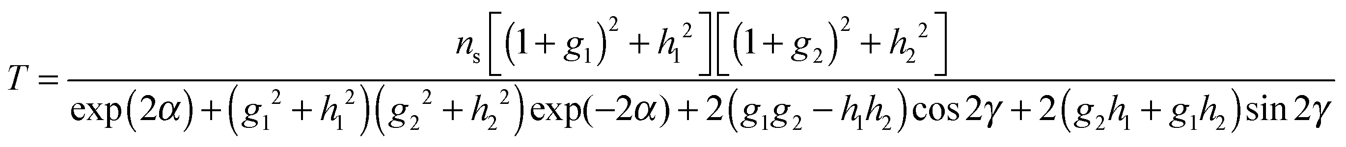
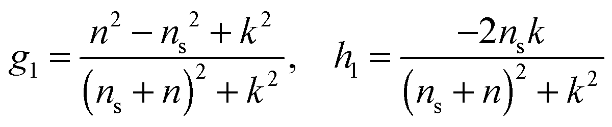
As shown in Fig. 1, our model system consists of a MoS2 film of thickness L deposited on a semi-infinite sapphire substrate. Yu et al. systematically measured the refractive index n and the extinction coefficient k of atomically thin MoS2 films. They found that both values of n and k are dependent on the film thickness, with the results tabulated in their work and used in our calculation.19 In the structure of a multilayer MoS2 film, the Mo atoms of an upper layer locate right above the S atoms of a lower layer, following an AB stacking sequence and having the crystal lattice of bulk 2H-MoS2.19,20 The sapphire substrate is considered as a non-absorbing medium of refractive index ns = ∼1.77 in the wavelength range of λ = 400–900 nm.21 The upper medium of the model system is air and the incident light is perpendicular to the sample surface. The reflectance R and transmittance T of the MoS2 film can then be calculated as18,22| |  | (1) |
| |  | (2) |
where
 |
| | Fig. 1 Schematic depiction of a MoS2 film with the refractive index n and the extinction coefficient k. The MoS2 film is deposited on a semi-infinite sapphire substrate. | |
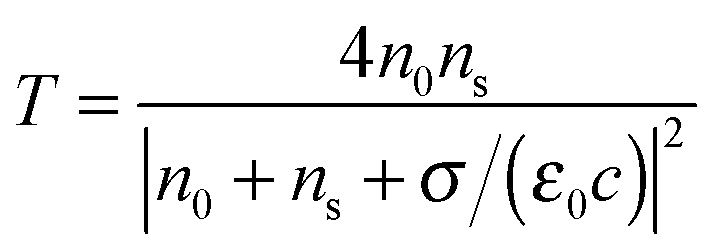
Note that an alternative approach to calculate the reflectance and transmittance of the MoS2 film involves the use of optical conductivity σ = σ1 + iσ2 of MoS2. By Maxwell's equations of the system with appropriate electromagnetic boundary conditions, R and T of the MoS2 film can be expressed as functions of optical conductivity18,23
| |  | (3) |
| |  | (4) |
where
n0 stands for the refractive index of the incident medium (here
n0 = 1.0 for air),
ε0 and
c are the free-space permittivity and light velocity, respectively. As a result, one can calculate the thickness-dependent reflectance and transmittance spectra of the MoS
2 film by
eqn (1) and (2). The real and imaginary parts of MoS
2 optical conductivity can then be deduced
via solving
eqn (3) and (4) with the calculated
R and
T. According to the previous thickness measurement for few-layered MoS
2 using an atomic force microscope,
19 the thicknesses of 1L, 2L, 3L, 4L, 5L, 6L, 7L, 8L, 9L and 10L MoS
2 films in our calculations are set as 0.65, 1.30, 1.90, 2.50, 3.10, 3.50, 4.30, 5.20, 5.60 and 6.20 nm, respectively.
Results and discussion
Fig. 2a and b show the reflectance and transmittance spectra of MoS2 films with various layer numbers. According to energy conservation, the frequency-dependent absorption A of the MoS2 films can also be calculated by R + T + A = 1. One can clearly see that monolayer MoS2 shows three peaks at 1.879, 2.016 and 2.867 eV in the reflectance spectra (corresponding to dips in the transmittance spectra), which originate respectively from the absorption of A, B and C excitons. The A and B excitonic peaks come from the direct transitions from two valence bands (which are split due to spin–orbit coupling) to the lowest conduction band at the K(K′) points, while the C excitonic peak arises from the indirect transition between the valence band maximum located at the Γ point and the conduction band minimum located at the Λ point of the Brillouin zone.6,19 As the layer number increases, the excitonic peaks gradually shift to lower energies. To clearly illustrate the layer dependence, Fig. 3a plots the peak energies of the A, B and C excitons as a function of the MoS2 film thickness. It is estimated that the energy difference between the A and B excitonic energies is approximately 140 meV for all thicknesses, being an indication of the strength of spin–orbit interaction.
 |
| | Fig. 2 (a) Reflectance and (b) transmittance spectra, (c) real and (d) imaginary parts of the optical conductivities for MoS2 films with different layer numbers. Legends are given in (a) and (b). Optical conductivity spectra in the dashed box are magnified by a factor of two. | |
 |
| | Fig. 3 Peak energies of the A, B and C excitons extracted from the reflectance spectra vs. (a) the MoS2 film thickness L and (b) 1/L2. Dashed lines in (a) are the fitting results obtained by using eqn (5). Dashed lines in (b) are simulated by using the model of infinite quantum wells. | |
Fig. 2c and d present the real and imaginary parts of the derived optical conductivities for the MoS2 films with various layer numbers. Possibly due to the band nesting effect as mentioned earlier,6,13 the σ1(σ2) spectra exhibit peaks at energies which are slightly larger (smaller) than the respective A, B and C excitonic energies. From low to high energies, the three peaks in σ1(σ2) spectra are labelled as σ1,A, σ1,B and σ1,C (σ2,A, σ2,B and σ2,C), indicating that they are associated with the corresponding excitonic transitions in MoS2, respectively. In our results, both σ1 and σ2 are positive, consistent with that reported by Morozov et al.18 To further confirm this observation, we measured the reflectance and transmittance of a monolayer MoS2 sample and derived its complex optical conductivity which has positive numbers for both σ1 and σ2 (see Fig. S1 in the ESI†). However, the sign of σ2 is contrary to the result reported by Wang et al.15 The negative σ2 observed by Wang et al. could partly be attributed to the significantly decreased mobility of charge carriers, because recombination of photoexcited carriers under ultrafast optical pump–probe beams can increase the carrier effective mass and the scattering probability.
Fig. 4a shows the peak energies induced by the A, B and C excitons in the optical conductivity for the MoS2 films with various layer numbers. One can see that the peaks of σ1,C and σ2,C gradually shift towards lower energies as the layer number increases, which appears to mimic the C excitonic resonance energies as observed in Fig. 3a. In particular, when the film thickness is larger than 4L, the energy difference between σ1,C (σ2,C) and C excitonic resonance energy exhibits a nearly linear dependence on L as shown in Fig. 4b. However, the peak energies of σ1,A and σ2,A (σ1,B and σ2,B) do not exhibit a similar blueshift with decreasing layer number down to 3L (2L) as shown in Fig. 4a and Table 1. As a result, no such linear dependence of energy difference between the optical conductivity peak and exciton energy on L can be observed for either the A or the B exciton for layer numbers >3L or 2L. These different effects of the A, B and C excitons in the optical conductivity spectra could be explained by the quantum confinement effect as discussed later.
 |
| | Fig. 4 (a) Excitonic resonance induced peak positions in optical conductivity spectra. Refer to the right (left) vertical axis for σ1,C and σ2,C (the others). (b) Energy differences between optical conductivity peaks and respective excitonic resonance energies. Dashed lines are just drawn as a guide to the eye. | |
Table 1 Peak positions of optical conductivities in MoS2 films with different layer numbers
| Layer number |
Peak position (eV) |
|
σ
1,A
|
σ
2,A
|
σ
1,B
|
σ
2,B
|
σ
1,C
|
σ
2,C
|
| 1 |
1.884 |
1.852 |
2.028 |
1.981 |
2.894 |
2.693 |
| 2 |
1.878 |
1.833 |
2.018 |
1.968 |
2.841 |
2.622 |
| 3 |
1.877 |
1.829 |
2.024 |
1.965 |
2.818 |
2.605 |
| 4 |
1.877 |
1.829 |
2.026 |
1.965 |
2.812 |
2.583 |
| 5 |
1.863 |
1.825 |
2.013 |
1.967 |
2.790 |
2.582 |
| 6 |
1.879 |
1.833 |
2.028 |
1.968 |
2.787 |
2.581 |
| 7 |
1.870 |
1.828 |
2.024 |
1.967 |
2.785 |
2.565 |
| 8 |
1.873 |
1.825 |
2.021 |
1.960 |
2.783 |
2.559 |
| 9 |
1.869 |
1.825 |
2.021 |
1.962 |
2.777 |
2.549 |
| 10 |
1.863 |
1.825 |
2.020 |
1.962 |
2.771 |
2.551 |
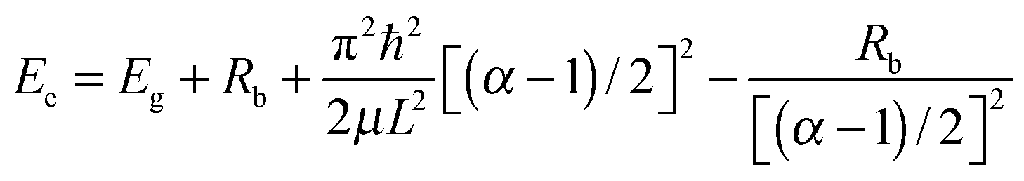
In the following text, we first evaluate the evolution of excitonic resonance peaks of MoS2 with film thickness, and fit the peak positions extracted from Fig. 2a by using the models of infinite quantum wells and the quantum wells in fractional dimensional space.19,24,25 For the MoS2 films thicker than 7L, the excitonic peak position Ee linearly depends on 1/L2 as presented in Fig. 3b. This matches well with the model of infinite quantum wells, and Ee can be fitted by Ee = Eg + π2ℏ2/2μL2, where Eg is the excitonic resonance energy in bulk MoS2 flake (Eg = 1.812, 1.966 and 2.616 eV for A, B and C excitons, respectively, according to Fig. 2a) and μ is the reduced electron–hole effective mass. The fitting results (dashed lines in Fig. 3b) give Ee = 1.812 + 0.781/L2, 1.966 + 0.577/L2 and 2.616 + 1.834/L2 for the A, B and C excitons, respectively. With these results we can derive the reduced masses for the A, B and C excitons in MoS2 films thicker than 7L, which are μ = 0.482m0, 0.652m0 and 0.205m0, respectively. We can also derive the Bohr radii of excitons by using aB = 0.0529m0ε/μ, where m0 is the free electron mass and ε = 10.71 is the static dielectric constant of bulk MoS2.26 The Bohr radii of A, B and C excitons are calculated to be 1.177, 0.869 and 2.763 nm, respectively. Since in the literature it lacks a comprehensive comparison about the physical parameters of the A, B and C excitons in MoS2 films, it may be difficult to thoroughly crosscheck all our calculated results. However, the derived μ values for the A and C excitons are reasonably in line with previously reported results which are 0.42m0 and 0.25m0 for bulk MoS2, respectively.19,27 Here the derived Bohr radii in thick/bulk MoS2 are also comparable with the previous experimental results which are ∼2.0 and ∼0.8 nm for the A and B excitons, respectively.28,29
For MoS2 films with layer numbers ≤7L, the excitonic peak positions deviate from the model of infinite quantum wells (see Fig. 3b). Instead, they could be fitted by the model of confined quantum wells with19,24,25
| |  | (5) |
where
Rb = 13.6
μ/
m0ε2 is the exciton binding energy in bulk MoS
2 and
α is a parameter to describe the dimensionality of the confined exciton. By using
eqn (5) to fit the excitonic peak positions in
Fig. 3a, we can get the effective dimensionality
α for the A, B and C excitons in 1L ∼ 7L MoS
2 films, as shown in
Table 2. It is seen that the
α value gradually increases from ∼2 for 1L to 3 for 8L, reasonably depicting the evolution of MoS
2 films from the 2D to 3D form. When
α equals to 3 for layer numbers ≥8L,
eqn (5) is naturally reduced to the equation for infinite quantum wells.
Table 2 Effective dimensionalities α and Bohr radii aB of excitons in different layer numbers of MoS2 films
| Layer number |
α
|
a
B (nm) |
| A exciton |
B exciton |
C exciton |
A exciton |
B exciton |
C exciton |
| 1 |
1.845 |
1.955 |
1.649 |
0.497 |
0.415 |
0.897 |
| 2 |
2.182 |
2.303 |
2.005 |
0.695 |
0.566 |
1.389 |
| 3 |
2.420 |
2.524 |
2.237 |
0.836 |
0.662 |
1.709 |
| 4 |
2.615 |
2.695 |
2.510 |
0.950 |
0.737 |
2.086 |
| 5 |
2.720 |
2.822 |
2.692 |
1.012 |
0.792 |
2.338 |
| 6 |
2.806 |
2.895 |
2.780 |
1.063 |
0.824 |
2.459 |
| 7 |
2.939 |
2.980 |
2.935 |
1.141 |
0.861 |
2.673 |
| ≥8 |
3.000 |
3.000 |
3.000 |
1.177 |
0.869 |
2.763 |
Using only the imaginary part of the dielectric function of MoS2, Yu et al. quantitatively fitted the peak position of the C exciton and extracted the related physical parameters as a function of the layer number.19 Nevertheless, they encountered bottleneck problems when dealing with the A and B excitons due to the fact that the peak positions of the A and B excitons exhibit no substantial layer dependence in the dielectric function. Interestingly, by substituting their measured dielectric functions into eqn (1), the calculated reflectance spectra (Fig. 2a) show that all the peaks of the A, B and C excitons gradually shift to lower energies with increasing layer number. Although the underlying physics for this observation needs further investigation, our calculation method can be used to extract the relevant physical parameters of the A, B and C excitons, and open up the opportunity to have a comprehensive comparison between them. For example, by using the α values given in Table 2, one can derive the effective exciton binding energy from Rb′ = 4Rb/(α − 1)2.25 Additionally, the effective Bohr radii of the excitons can also be obtained by utilizing aB′ = aB(α − 1)/2,25 as shown in Table 2.
Here we should point out that there are strong interface couplings, e.g., van der Waals interaction, in the few-layered MoS2 and between the monolayer MoS2 and the substrate. Moreover, the functional form of electron–hole interaction could be modified by the nonlocal nature of dielectric screening.30,31 Thus the borrowing of eqn (5) which assumes a homogeneous quantum well to 2D materials is essentially an approximation. This may also be the reason why the values of α in Table 2 for the three excitons of the monolayer MoS2 are smaller than 2. By using the dielectric screened hydrogen model,30,31 the effective binding energy of the C exciton in the monolayer MoS2 is calculated to be 0.72 eV. Substituting this value instead of Rb′ into eqn (5), we deduce the value of α to be 1.934. It is clear that the incorporation of a dielectric screening effect makes a more reasonable value for α. In order to obtain an accurate dimensionality, taking into account the interface couplings as well as the effect of dielectric screening on the confinement energy [the third term in eqn (5)] may be necessary. This may need more complicated theoretical studies. Even so, we believe that the simplicity is the merit of eqn (5). Besides, the model of confined quantum wells leaves out many other influence factors, making it feasible to solely inspect the quantum confinement effect.
Fig. 5 shows the extracted Bohr radii aB′ as a function of the film thickness. One can see that the C exciton has the largest Bohr radius while the B exciton gives the smallest size in the same thickness of MoS2 film. Furthermore, the Bohr radius of the C exciton rapidly decreases with reducing thickness after the film thins to 7L, whereas, the decreasing rates of the A and B excitonic radii are relatively slower than C. In a semiconductor crystal, an exciton will experience strong or weak quantum confinement when the semiconductor thickness is less or greater than double the Bohr radius of the exciton.32 The sizes of the A, B and C excitons in the thick/bulk MoS2 are 2aB = ∼2.35, ∼1.74 and ∼5.53 nm, respectively. They are close to the thicknesses of 3L, 2L and 8L MoS2 films, i.e., 1.90, 1.30 and 5.20 nm, respectively. As a consequence, the A, B and C excitons in thin MoS2 films are expected to experience a strong quantum confinement effect. However, the C exciton is more tightly confined in most of the films studied in our work while the A and B excitons can be confined only in films thinner than 4L and 3L, respectively. The variation in the C excitonic radius presents the largest range as the layer number decreases to 1L (see Fig. 5), implying that the excitonic quantum confinement plays the strongest effect on the C exciton in comparison with the A and B excitons. As a result, the peaks of σ1,C and σ2,C gradually shift towards lower energies with increasing layer number (Fig. 4a) and the energy difference between the σ1,C (σ2,C) peak and C excitonic resonance energy linearly depends on the thickness for films thicker than 4L (see Fig. 4b). In sharp contrast, the peak positions of σ1,A and σ2,A (σ1,B and σ2,B) fluctuate with the layer number when the MoS2 film is thicker than 3L (2L), as shown in Fig. 4. Note that the fluctuation of the energy difference σ1,C,peak − Cpeak (or Cpeak − σ2,C,peak) in films thinner than 5L could be a result of substrate-induced van der Waals interaction and/or the local doping effect.33,34 Previous studies have shown that the energy variation in the excitonic peak position induced by the influence of the substrate could be up to ∼80 meV for a bilayer MoS2 film, and this kind of influence decreases significantly with increasing the layer number.33,34
 |
| | Fig. 5 Bohr radii of A, B and C excitons vs. the MoS2 film thickness. Dashed lines are just drawn as a guide to the eye. | |
In addition to the effect in the peak position of MoS2 optical conductivity, our results further show that the excitonic quantum confinement phenomenon also has a strong influence in the excitonic peak intensity and the magnitudes of σ1,A, σ1,B and σ1,C (σ2,A, σ2,B and σ2,C). Intuitively, it is reasonable that the reflectance intensity and the optical conductivity magnitude decrease upon reducing the MoS2 film thickness. By using the measured dielectric function, e.g., the n and k values for bulk MoS2, the calculation results (see Fig. S2 in the ESI†) show that both reflectance intensity and optical conductivity decrease linearly upon decreasing the film thickness. By contrast, if we take into account the excitonic quantum confinement effect, we find that both of them induced by the A, B and C excitons, as shown in Fig. 6, are attenuated by reducing the film thickness, following an exponential function
where
I stands for the intensity or magnitude,
a,
b and
c are fitting coefficients with detailed values given in
Table 3. Comparing the results in
Fig. 6 and Fig. S2 (ESI
†) reveals that the excitonic quantum confinement effect significantly accelerates the decay of the exciton-induced reflectance peak intensity and the optical conductivity peak magnitude for MoS
2 of the same thickness. Since most of the previous studies on 2D TMDCs were limited to the film with the maximum layer number of 5L, they failed to give a useful empirical formula to predict the peak magnitude of optical conductivity.
Eqn (6) and
Table 3 may provide guidelines to the evolution of the optoelectronic properties of the A, B and C excitons with MoS
2 film thickness.
 |
| | Fig. 6 (a) Reflectance intensities and (b) magnitudes of optical conductivity induced by A, B and C excitons vs. the MoS2 film thickness. Symbols are the results extracted from Fig. 2. Dashed lines are the fitting results obtained by using eqn (6). | |
Table 3 Detailed values of fitting coefficients a, b and c in eqn (6)
| |
Reflectance |
Optical conductivity |
| A exciton |
B exciton |
C exciton |
σ
1,A
|
σ
2,A
|
σ
1,B
|
σ
2,B
|
σ
1,C
|
σ
2,C
|
|
a
|
−2.5056 |
−2.5100 |
−2.2470 |
0.6572 |
1.4621 |
0.8487 |
1.3611 |
2.1269 |
1.8121 |
|
b
|
0.0961 |
0.1366 |
0.2663 |
0.3895 |
0.4992 |
0.4653 |
0.5355 |
0.4945 |
0.5252 |
|
c
|
0.0154 |
0.0094 |
−0.0073 |
0.0077 |
−0.0189 |
−0.0160 |
−0.0232 |
−0.0208 |
−0.0234 |
Conclusions
In summary, the layer-dependent optical conductivities of MoS2 films have been derived from their calculated reflectance and transmittance spectra in the visible to near-infrared region. It is found that the C exciton has the largest Bohr radius in the same thickness of MoS2 film such that it is subjected to the strongest quantum confinement effect compared with the A and B excitons. As a result, both peak positions of real and imaginary parts of the optical conductivity induced by the C exciton gradually shift towards high energies with decreasing film thickness. In remarkable contrast, this blueshift tendency is not observed for either the A or the B exciton for films thicker than 3L or 2L, respectively. Additionally, our results reveal that the attenuations of reflectance intensity and the magnitude of optical conductivity induced by the A, B and C excitons follow an exponential decaying function with decreasing MoS2 film thickness. These findings may provide important insights into the critical role of the excitonic quantum confinement effect in the photoelectric properties of 2D TMDCs in general. The fitting equations along with the derived physical parameters may also provide useful guidelines for future applications of MoS2 materials in 2D nanodevice fabrications.
Acknowledgements
We gratefully acknowledge Dr Yiling Yu and Prof. Linyou Cao from North Carolina State University who shared their measured optical constants of bulk MoS2. We are also grateful to Mr Chang Qin from 6Carbon Technology for his help with the preparation of the monolayer MoS2 film on the sapphire substrate. We acknowledge the financial support from the Hong Kong Polytechnic University (Grant No. 1-ZVCG).
Notes and references
- G. R. Bhimanapati, Z. Lin, V. Meunier, Y. Jung, J. Cha, S. Das, D. Xiao, Y. Son, M. S. Strano, V. R. Cooper, L. Liang, S. G. Louie, E. Ringe, W. Zhou, S. S. Kim, R. R. Naik, B. G. Sumpter, H. Terrones, F. Xia, Y. Wang, J. Zhu, D. Akinwande, N. Alem, J. A. Schuller, R. E. Schaak, M. Terrones and J. A. Robinson, ACS Nano, 2015, 9, 11509–11539 CrossRef CAS PubMed.
- R. Ganatra and Q. Zhang, ACS Nano, 2014, 8, 4074–4099 CrossRef CAS PubMed.
- X. D. Li, S. Q. Wu and Z. Z. Zhu, J. Mater. Chem. C, 2015, 3, 9403–9411 RSC.
- X. H. Wang, J. Q. Ning, C. C. Zheng, B. R. Zhu, L. Xie, H. S. Wu and S. J. Xu, J. Mater. Chem. C, 2015, 3, 2589–2592 RSC.
- Y. Li, N. Dong, S. Zhang, K. Wang, L. Zhang and J. Wang, Nanoscale, 2016, 8, 1210–1215 RSC.
- D. Kozawa, R. Kumar, A. Carvalho, K. K. Amara, W. Zhao, S. Wang, M. Toh, R. M. Ribeiro, A. H. Castro Neto, K. Matsuda and G. Eda, Nat. Commun., 2014, 5, 4543 CAS.
- Y. C. Wu, C. H. Liu, S. Y. Chen, F. Y. Shih, P. H. Ho, C. W. Chen, C. T. Liang and W. H. Wang, Sci. Rep., 2015, 5, 11472 CrossRef CAS PubMed.
- N. Perea-López, Z. Lin, N. R. Pradhan, A. Iñiguez-Rábago, A. L. Elías, A. McCreary, J. Lou, P. M. Ajayan, H. Terrones, L. Balicas and M. Terrones, 2D Mater., 2014, 1, 011004 CrossRef.
- P. Li, B. Liang, M. Su, Y. Zhang, Y. Zhao, M. Zhang, C. Ma and N. Su, Appl. Phys. B: Lasers Opt., 2016, 122, 150 CrossRef.
- Y. G. Kim, K. C. Kwon, Q. V. Le, K. Hong, H. W. Jang and S. Y. Kim, J. Power Sources, 2016, 319, 1–8 CrossRef CAS.
- J. Yang, Z. Wang, F. Wang, R. Xu, J. Tao, S. Zhang, Q. Qin, B. Luther-Davies, C. Jagadish, Z. Yu and Y. Lu, Light: Sci. Appl., 2016, 5, e16046 CrossRef CAS.
- Z. Wu, E. Taylor and E. Zaremba, Europhys. Lett., 2015, 110, 26002 CrossRef.
- A. Carvalho, R. M. Ribeiro and A. H. Castro Neto, Phys. Rev. B: Condens. Matter Mater. Phys., 2013, 88, 115205 CrossRef.
- H. Wang, C. Zhang and F. Rana, Nano Lett., 2015, 15, 339–345 CrossRef CAS PubMed.
- H. Wang, C. Zhang and F. Rana, Nano Lett., 2015, 15, 8204–8210 CrossRef CAS PubMed.
- Z. Li and J. P. Carbotte, Phys. Rev. B: Condens. Matter Mater. Phys., 2012, 86, 205425 CrossRef.
- H. Rostami and R. Asgari, Phys. Rev. B: Condens. Matter Mater. Phys., 2014, 89, 115413 CrossRef.
- Y. V. Morozov and M. Kuno, Appl. Phys. Lett., 2015, 107, 083103 CrossRef.
- Y. Yu, Y. Yu, Y. Cai, W. Li, A. Gurarslan, H. Peelaers, D. E. Aspnes, C. G. Van de Walle, N. V. Nguyen, Y.-W. Zhang and L. Cao, Sci. Rep., 2015, 5, 16996 CrossRef CAS PubMed.
- Y. Yu, C. Li, Y. Liu, L. Su, Y. Zhang and L. Cao, Sci. Rep., 2013, 3, 1866 Search PubMed.
- Refractive index database: http://refractiveindex.info/?shelf=main&book=Al2O3&page=Malitson-o.
- O. S. Heavens, Rep. Prog. Phys., 1960, 23, 1–65 Search PubMed.
- T. Stauber, N. M. R. Peres and A. K. Geim, Phys. Rev. B: Condens. Matter Mater. Phys., 2008, 78, 085432 CrossRef.
- X. F. He, Phys. Rev. B: Condens. Matter Mater. Phys., 1990, 42, 11751–11756 CrossRef.
- X. F. He, Phys. Rev. B: Condens. Matter Mater. Phys., 1991, 43, 2063–2069 CrossRef.
- A. Thilagam, J. Appl. Phys., 2014, 116, 053523 CrossRef.
- E. Fortin and F. Raga, Phys. Rev. B: Condens. Matter Mater. Phys., 1975, 11, 905–912 CrossRef CAS.
- R. F. Frindt, Phys. Rev., 1965, 140, 536–539 CrossRef CAS.
- T. Sekine, K. Uchinokura, T. Nakashizu, E. Matsuura and R. Yoshizaki, J. Phys. Soc. Jpn., 1984, 53, 811–818 CrossRef CAS.
- T. Olsen, S. Latini, F. Rasmussen and K. S. Thygesen, Phys. Rev. Lett., 2016, 116, 056401 CrossRef PubMed.
- S. Latini, T. Olsen and K. S. Thygesen, Phys. Rev. B: Condens. Matter Mater. Phys., 2015, 92, 245123 CrossRef.
-
D. W. Snoke, Solid State Physics: Essential Concepts, Pearson/Addison-Wesley, 2009 Search PubMed.
- M. Buscema, G. A. Steele, H. S. J. van der Zant and A. Castellanos-Gomez, Nano Res., 2014, 7, 561–571 CrossRef.
- N. Scheuschner, O. Ochedowski, A.-M. Kaulitz, R. Gillen, M. Schleberger and J. Maultzsch, Phys. Rev. B: Condens. Matter Mater. Phys., 2014, 89, 125406 CrossRef.
Footnote |
| † Electronic supplementary information (ESI) available: Experimentally measured complex optical conductivity of a monolayer MoS2 film, and calculated thickness-dependent reflectance intensity and magnitude of optical conductivity without considering the excitonic effect. See DOI: 10.1039/c6tc02502a |
|
| This journal is © The Royal Society of Chemistry 2016 |
Click here to see how this site uses Cookies. View our privacy policy here. 
 Open Access Article
 This Open Access Article is licensed under a Creative Commons Attribution-Non Commercial 3.0 Unported Licence