
Crystal organometal halide perovskites with promising optoelectronic applications
Junnian
Chen
a,
Shasha
Zhou
a,
Shengye
Jin
b,
Huiqiao
Li
a and
Tianyou
Zhai
*a
aState Key Laboratory of Material Processing and Die & Mould Technology, School of Materials Science and Engineering, Huazhong University of Science and Technology, Wuhan 430074, P. R. China. E-mail: zhaity@hust.edu.cn
bState Key Laboratory of Molecular Reaction Dynamics, Dalian Institute of Chemical Physics, Chinese Academy of Sciences, Dalian, Liaoning 116023, P. R. China
First published on 18th November 2015
Abstract
Organometal halide perovskites AMX3 (A = organic cation, M = metal cation, and X = halogen anion) have been dominating the photovoltaic fields with an unexpected sharp efficiency enhancement to 20.1% in the past five years. Furthermore, the extraordinary properties of optical absorption, photoluminescence and low non-radiative recombination rates extend their applications into optoelectronic fields beyond photovoltaic devices. This review briefly outlines the state-of-the-art research activities of crystal perovskite AMX3, describes the fundamental optoelectronic properties, specific morphologies and related synthesis techniques, and summarizes their functions in optoelectronic fields such as solar cells, lasers, light-emitting diodes and photodetectors. Finally, the general challenges and the potential future directions of this exciting research area are highlighted.
 Junnian Chen | Junnian Chen received her BS degree in Applied Chemistry from Huazhong Agricultural University in 2009, and then received her PhD degree in Inorganic Chemistry from Wuhan University under the supervision of Prof. Tianyou Peng in 2014. Currently, she is working as a postdoctoral fellow in Prof. Tianyou Zhai's group at School of Materials Science and Engineering, Huazhong University of Science and Technology (HUST). Her scientific research concentrates on the preparation of quasi solid state electrolytes for dye-sensitized solar cells, as well as micro/nano-structured organometal halide perovskites for optoelectronic devices. |
 Shasha Zhou | Shasha Zhou received her BS degree in Materials Science and Engineering from Huazhong University of Science and Technology (HUST) in 2014. Currently, she is a graduate student in Prof. Tianyou Zhai's group at School of Materials Science and Engineering, HUST. Her scientific research concentrates on the preparation of transition metal dichalcogenides and their promising applications in energy science. |
 Shengye Jin | Shengye Jin received his BS degree in Chemical Engineering from Dalian University of Technology in 2001, MS degree in Chemistry from Dalian Institute of Chemical Physics (DICP)-CAS in 2004, and PhD in Physical Chemistry from Emory University (USA) in 2010. He did postdoctoral research at Argonne National Laboratory and Northwestern University from 2010 to 2013, where he worked on photochemical dynamics of various materials for solar energy conversion. Dr Jin then joined the State Key Laboratory of Molecular Reaction Dynamics of Dalian Institute of Chemical Physics (DICP)-CAS in 2013. He is now a professor and group leader of the ultrafast time-resolved spectroscopy and dynamics research group in DICP. His research focuses on the study of photoinduced reaction dynamics in materials for solar energy conversion by using ultrafast time-resolved spectroscopy and optical imaging technology. |
 Huiqiao Li | Huiqiao Li received her BS degree in chemistry from Zhengzhou University in 2003, and then received her PhD degree in physical chemistry from Fudan University in 2008. Afterwards, she worked as a postdoctoral fellow in Prof. Haoshen Zhou's group for 4 years at Energy Technology Research Institute, National Institute of Advanced Industrial Science and Technology (AIST), Japan. Currently, she is a full Professor of School of Materials Science and Engineering, Huazhong University of Science and Technology (HUST). Her research interests include energy storage materials and electrochemical power sources. She has authored and co-authored over 40 refereed journal publications, 1 book chapter, and 8 patents. Her publications have been cited more than 2500 times (H-index is 22). |
 Tianyou Zhai | Tianyou Zhai received his BS degree in chemistry from Zhengzhou University in 2003, and then received his PhD degree in physical chemistry from the Institute of Chemistry, Chinese Academy of Sciences (ICCAS) under the supervision of Prof. Jiannian Yao in 2008. Afterwards he joined in National Institute for Materials Science (NIMS) as a JSPS postdoctoral fellow of Prof. Yoshio Bando's group and then as an ICYS-MANA researcher within NIMS. Currently, he is a Chief Professor of School of Materials Science and Engineering, Huazhong University of Science and Technology (HUST). His research interests include the controlled synthesis and exploration of fundamental physical properties of inorganic functional nanomaterials, as well as their promising applications in energy science, electronics and optoelectronics. He has authored and co-authored above 100 peer-reviewed journal articles, 5 book chapters, co-edited 1 book on nanotechnology, and held 7 patents. His publications have been cited more than 5000 times (H-index is 40). |
1 Introduction
Organometal halide perovskites, described by AMX3 (A = organic cation, M = metal cation, and X = halogen anion) are direct bandgap semiconductors that combine the advantages of crystalline inorganic compounds with those of organic molecules within a molecular-scale composite, possessing attributes of easy process and high carrier mobility.1 Initial investigations on organometal halide perovskites mainly focus on the synthesis2,3 and fundamental properties.4–6 In the early 1990s, crystal organometal halide perovskite based field-effect transistors (FETs) and light-emitting diodes (LEDs)7,8 with good performances were first reported by Mitzi and co-workers, resulting from their outstanding optoelectronic properties.9–11 After Miyasaka et al. fabricated the initial CH3NH3PbX3 solar cell in 2009,12 perovskite materials have become the prime popular light absorbent. Attributing to the unique properties of strong optical absorption and low non-radiative carrier recombination rates, perovskites AMX3 renovated the solar cell field in the past five years with the energy conversion efficiency jumped from 3.8% to 20.1%.13–17 Closely following the rapid development of perovskite solar cells, perovskite film with excellent optoelectronic properties,18,19 bulk single crystals with low defect density20 and low dimensional crystals with specific morphologies21–23 evoked new research interest in the applications of LEDs and photodetectors. A LED incorporating low-cost organometal halide perovskite with a high luminance of 417 cd m−2 has been achieved at room temperature, indicating huge potential for large scale production.24 Besides, a hybrid perovskite photodetector with a large detectivity approaching 1014 Jones, a linear dynamic range over 100 decibels (dB) and a fast photoresponse with 3 dB bandwidth upto 3 MHz has been demonstrated as well, suggesting great promise in photodetectors.25 Wavelength-tunable nanowire perovskite CH3NH3PbX3 (X = CI, Br, I) lasing with low threshold (220 nJ cm−2) and high quality factor (Q ∼ 3600) has been observed at room-temperature, making lead halide perovskite an ideal material for the development of modern optoelectronic devices down to a nanoscale.26 Thus, research studies on crystal organometal halide perovskites have grown very rapidly in recent years, as illustrated in Fig. 1. However, recent reviews are mainly concentrated on the photovoltaic applications of organometal halide perovskites,27–30 and few have focused on the research progress of organometal halide perovskites in the optoelectronic field as well as the recent development of this kind of material. | ||
| Fig. 1 Publication statistics with respect to perovskites AMX3. The data was compiled on 23rd 9, 2015 using the ISI database and by applying topic = (perovskite) and topic = (organic inorganic). | ||
In this review, we will provide a summary of the state-of-the-art crystal perovskite material, focusing mainly on the facile synthesis, crystal morphology, unique properties and related optoelectronic applications. We will begin with a historical background of perovskites AMX3, followed by the description of their fundamental structures, optical and electronic properties. Subsequently, we will introduce crystalline perovskites AMX3 with specific morphologies and their corresponding synthesis methods. Next, we will exhibit the recent achievements regarding the potential applications of crystal perovskites AMX3 in LEDs, lasers, field emitters and photodetectors, etc. (Fig. 2). Finally, we will conclude this review with some perspectives and outlook on the development of perovskite material in the near future. Overall, this comprehensive review will provide a summary into the rapid development of crystal perovskite material and their amazing success in the optoelectronic field.
 | ||
| Fig. 2 Schematic diagram showing the potential optoelectronic properties and applications of typical perovskite AMX3 (acronyms: QD: quantum dots, NW: nanowire, NR: nanorod, NC: nanocrystal, MC: millimeter-scale crystal, NP: nanoparticle, PL: photoluminescence, EL: electroluminescence, LEDs: light-emitting diodes, FET: field-effect transistor and LECs: light-emitting electrochemical cells). | ||
2 Fundamental properties of crystal organometal halide perovskites
Organometal halide perovskite AMX3, isostructural to perovskite CaTiO3 and related oxides, possesses diversity in composition, structure and properties. As can be seen in Fig. 3a, perovskite AMX3 exhibits a three-dimensional (3-D) network of corner-sharing MX6 octahedra where a cation occupying the cuboctahedral cavity maintaining the electronegativity of the system.31 The structural probability and crystallographic stability of perovskite AMX3 can be evaluated via a tolerance factor t and an octahedral factor μ.32t is defined as the ratio of the distance A–X to B–X in an idealized solid-sphere model: | (1) |
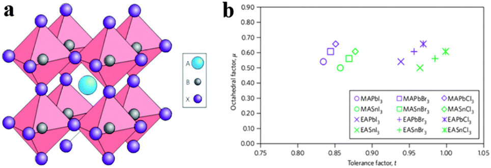 | ||
| Fig. 3 Perovskite AMX3 crystal structure and related tolerance and octahedral factors. (a) Crystal structure of cubic perovskite ABX3. (b) t and μ factors for 12 common organometal halide perovskites. Reproduced from ref. 31 with permission. Copyright 2014 Nature Publishing Group. | ||
2.1 Optical properties
As the unique attribute of organometal halide perovskites, optical properties of photo-generated charge carriers have been intensively investigated on their strength and resonant behaviour.35,36 Benefiting from the large exciton binding energy of perovskites CH3NH3PbX3 (X = halogen) and their mixed-halide crystals, they show clear excitonic absorption and free-excitonic emission in the visible region at room temperature.35 Characteristic excitonic absorption peaks in perovskite could be tailored to virtually any wavelength in the visible spectrum through adjusting the metal atom (Ge, Sn, and Pb), halogen (Cl, Br, and I) or inorganic sheet thickness.37 Typical perovskite CH3NH3PbI3 exhibits a remarkably steep absorption onset at 825 nm (1.5 eV) with a large absorbance coefficient of about 5 × 105 cm−1, which is upto 1 order of magnitude higher than that of GaAs within the visible light range.38 Further replacing the organic cation of methylammonium (MA) lead iodide with formamidinium (FA), the energy bandgap could be tuned down to 1.48 eV (FAPbIyBr3−y) (840 nm absorption onset).39 The onset absorption band of FAPbIyBr3−y (FA = HC(NH2)2+, 0 ≤ y ≤ 1) can be tuned from 838 nm (1.48 eV) to 556 nm wavelength (2.23 eV), and an increase in iodide fraction will gradually red-shift the onset absorption band of FAPbIyBr3−y (Fig. 4a). The broad and strong light absorbance in the visible wavelength range elects organometal halide perovskites as the popular semiconductor in the optoelectronic field.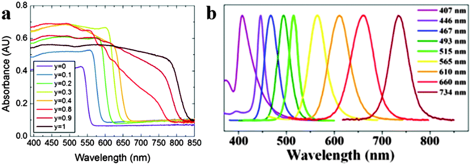 | ||
| Fig. 4 Absorbance and PL spectra of perovskites. (a) UV-Vis absorption spectra of FAPbIyBr3−y perovskites. Reproduced from ref. 39 with permission. Copyright 2014 Royal Society of Chemistry. (b) The emission spectra of CH3NH3PbX3 QDs. Reproduced from ref. 43 with permission. Copyright 2015 American Chemical Society. | ||
Furthermore, organometal halide perovskites could also emit strong room-temperature photoluminescence (PL) that arises from excitons (radiative recombination of charge carriers) in the inorganic sheets.40,41 Generally, organometal halide perovskite methylammonium lead halide (CH3NH3PbX3) and the partially halide-substituted mixed halides emit strong and broad PL around their band gap energies. Pb perovskites composed of (CH3NH3+) or (HC(NH2)2+) cations and iodide (anion) emit between 700 and 800 nm while the emission of similar Sn perovskites lie within 850–1000 nm, covering a broad region of the near-IR spectrum.42 Just as optical absorption, the PL of organometal halide perovskites could be affected through modifying organic cations or halide anions. As shown in Fig. 4b, the PL spectra of CH3NH3PbX3 QD could be finely tuned from 407 to 734 nm by tailoring the composition of halide anions.43 PL spectroscopy could reflect some important photo-physical properties such as low exciton binding energies44,45 and high dielectric constants,46,47 particularly valuable for the optoelectronic property characterization of perovskites. The strong and tunable PL indicates that organometal halide perovskites are suitable for a range of light-emitting applications, including lasers, light-emitting devices and optical sensors.
2.2 Electrical properties
In addition to the remarkable optical properties, electrical properties of organometal halide perovskites have caught the attention of scientists as well.48–50 The basic electrical properties such as carrier type, concentration and mobility in perovskites were proved to be greatly influenced by their synthesis methods.51,52 Through investigating the nature of organometal halide perovskites fabricated from a variety of synthetic approaches, Stoumpos et al. observed that n-type perovskites with the lowest carrier concentration are gained from solution and p-type perovskites can be obtained through solid state reactions.42 Based on the resistivity, Seebeck and Hall effect investigation, polycrystalline CH3NH3PbI3 was demonstrated to show n-type conductivity, a carrier concentration of ∼109 cm−3 and an electron mobility of 66 cm2 V−1 s−1. While CH3NH3SnI3 synthesized by the solution processed method shows an electron mobility of 200 cm2 V−1 s−1,52 which is much smaller than the 2320 cm2 V−1 s−1 measured for solid-state reaction in a vacuum-sealed tube.42 Besides, the high electrical conductivity of CH3NH3Sn1−xPbxBr3 was found to decrease drastically upon replacement of Sn by Pb, due to the change in the local octahedral environment of SnBr6 and the Sn–Br–Sn bond length.53Yang et al. reported the significance of ionic transport in organic lead-iodide based perovskites, and observed higher ionic conductivity than electronic conductivity in CH3NH3PbI3.54 Single distorted semicircle appears in the alternating-current (AC) impedance spectra (Fig. 5a), which is assigned to the pure bulk property (εr,∞ = 34 at 308 °C) based on the calculated relative dielectric constant.48 As can be seen in Fig. 5b, εr,∞ slightly decreases with the increasing temperature. Bulk conductivity of CH3NH3PbI3 increases as temperature goes up with an activation energy of 0.43 eV, in accordance with the previous report.55 As temperature increases, the real part of the complex permittivity (εr′) in high frequencies (>104 Hz) slightly decreases (Fig. 5c). In the lower frequency range, εr′ begins to rapidly increase by an order of magnitude upto 300 at 1 Hz and 30 °C and increases with the increased temperature at low frequencies, which resembles the phenomenon observed from MAPbI3-based solar cells.56 In addition, electrical properties of perovskites have been proved to be affected by the size of the organic cation.
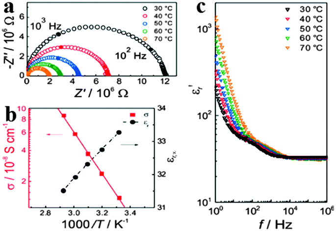 | ||
| Fig. 5 Electrical properties of MAPbI3. (a) Alternating-current impedance spectra of MAPbI3. (b) Conductivity σ and the bulk relative dielectric constant εr,∞ as a function of temperature. (c) Frequency dependent εr′ (the real part of the complex permittivity). Reproduced from ref. 54 with permission. Copyright 2015 Wiley-VCH. | ||
Even in polycrystalline film, organometal halide perovskites with low-cost and low defect density could offer significant advantages over the conventional semiconductors. The extraordinary optical and electronic properties make perovskite a unique semiconductor. Moreover, organometal halide perovskites with chemical tunability of optoelectronic properties could be tailored for various requirements, which have and will continually arouse intensive interest in the optoelectronic field.
3 Synthesis of crystal organometal halide perovskites
Synthesis of crystal organometal halide perovskite was first reported by Weber in 1978, who fabricated the cubic perovskite CH3NH3PbX3 through mixing of the precursor CH3NH3 aqueous, concentrated Br2 aqueous and Pb(NO3)2 under stirring at 100 °C.57 Later, a convenient two-step technique for preparing organometal halide perovskite thin films was developed, during which films of the metal halide MI2 were deposited onto ash glass or quartz disks using vacuum evaporation or spin-coating and followed by dipping into an organic ammonium iodide solution within a short time at room temperature.58 With further development of organometal halide perovskites, solution processed59,60 and vapor evaporation61 methods have become the two main effective methods for preparation of perovskites.3.1 Solution processed methods
Crystal organometal halide perovskites could be easily precipitated from solution through evaporating the precursor metal halide and organic halide by heating or spin-coating. As stated above, a heating approach was developed for fabrication of crystal perovskite early in the 1970s.57 While a spin-coating technique is frequently employed in the preparation of perovskite film after the birth of perovskite solar cells.13,25,62,63 Common solvents used for the synthesis of perovskites include γ-butyrolactone (GBL), N,N-dimethylformamide (DMF) and dimethylsulphoxide (DMSO). By coating the simply mixed CH3NH3I and PbI2 (in a GBL solution with a stoichiometric (1![[thin space (1/6-em)]](https://www.rsc.org/images/entities/char_2009.gif) :1) molar ratio) and CH3NH3Br and PbBr2 (in a DMF) onto TiO2 film, CH3NH3PbI3 and CH3NH3PbBr3 perovskite polycrystalline thin film could be easily obtained at room temperature.12 Besides, iodide/chloride mixed-halide perovskite CH3NH3PbIxCl3−x film was achieved through spin-coating dissolved MAI and PbCl2 (3:1 molar ratio) or MACl and PbI2 (1:1 molar ratio) in anhydrous DMF at room temperature.64 Through introducing the toluene drop-casting process after spin-coating precursors in a mixed solvent of GBL and DMSO, Jeon et al. obtained extremely uniform and dense perovskite MAPb(I1−xBrx)3 layers.65 The novel solvent-engineering technology provides us new insight into improving the quality of perovskite film. However, the above single-step solution process easily causes uncontrollable precipitation of the perovskites and leads to large morphological variations. Thus a two-step solution process emerged in which the lead halide is prepared by spin-coating and then exposed to methylammonium halide for converting into perovskites through spin-coating66 or dip-coating,67 gaining better control over the morphology of perovskite films. Mixed-cation perovskite (MA)x(FA)1−xPbI3 was successfully synthesized via exposure of PbI2 infiltrated TiO2 to a solution of FAI and MAI in 2-propanol.68 Furthermore, employment of the solvent annealing technique after a two-step solution process was proved to effectively increase the crystallinity and grain size of CH3NH3PbI3 film.66
:1) molar ratio) and CH3NH3Br and PbBr2 (in a DMF) onto TiO2 film, CH3NH3PbI3 and CH3NH3PbBr3 perovskite polycrystalline thin film could be easily obtained at room temperature.12 Besides, iodide/chloride mixed-halide perovskite CH3NH3PbIxCl3−x film was achieved through spin-coating dissolved MAI and PbCl2 (3:1 molar ratio) or MACl and PbI2 (1:1 molar ratio) in anhydrous DMF at room temperature.64 Through introducing the toluene drop-casting process after spin-coating precursors in a mixed solvent of GBL and DMSO, Jeon et al. obtained extremely uniform and dense perovskite MAPb(I1−xBrx)3 layers.65 The novel solvent-engineering technology provides us new insight into improving the quality of perovskite film. However, the above single-step solution process easily causes uncontrollable precipitation of the perovskites and leads to large morphological variations. Thus a two-step solution process emerged in which the lead halide is prepared by spin-coating and then exposed to methylammonium halide for converting into perovskites through spin-coating66 or dip-coating,67 gaining better control over the morphology of perovskite films. Mixed-cation perovskite (MA)x(FA)1−xPbI3 was successfully synthesized via exposure of PbI2 infiltrated TiO2 to a solution of FAI and MAI in 2-propanol.68 Furthermore, employment of the solvent annealing technique after a two-step solution process was proved to effectively increase the crystallinity and grain size of CH3NH3PbI3 film.66
Song et al. investigated the formation of the perovskite MAPbI3 phase via carrying out a systematic study on the structural and optical properties of crystal perovskites fabricated by spin-coating MAI and PbI2 precursor solutions with different mole fractions, revealing that the obtained MAPbI3 phases were strongly dependent on the reaction temperature and initial compositions.69 Unexpectedly, chloride as a dopant in precursor solution could offer some unexpected improvement in the film morphology and structure,70,71 and further work on the mechanism is essential. In conclusion, exploring the controllable solution processed method for synthesizing perovskite films of uniform, continuous and pinhole-free is still challenging and remains a chief concern.
Along with the development of perovskite polycrystalline films, single crystal perovskites with high quality and purity have also been successfully synthesized. The solution processed method has been proved to be an effective method of growing single crystal perovskites.9,10 Early in the 1990s, [NH2C(I) = NH2]3MIs crystals were obtained by slowly cooling concentrated hydroidic acid aqueous containing NH2CN and MI2 (M = Sn, Pb) in an argon atmosphere.3 Later, Mitzi et al. successfully synthesized single crystal perovskite (C6H5C2H4NH3)2PbCl4 at room temperature by using a layered solution approach through addition of C6H5C2H4NH2 onto the top of methanol.9 Recently, bulk single crystal perovskites of high purity with less grains, boundaries, voids, and surface defects emerged as popular material.72–75 Dong et al. synthesized bulk single crystal perovskite CH3NH3PbI3 from a supersaturated CH3NH3PbI3 solution by using a temperature gradient top-seeded-solution-growth method.76 The schematic device for growing single crystal CH3NH3PbI3 is illustrated in Fig. 6a. The large MAPbI3 single crystals (MSCs) were obtained by the consumption of small MSCs in the bottom, attributing to the small temperature difference between the bottom and top of the solution that induced sufficient convection. Single crystal CH3NH3PbI3 exhibits a length and a height of 10 and 3.3 mm, respectively (Fig. 6b and c). By employing an antisolvent vapor-assisted crystallization approach, Shi et al. obtained sizable crack-free CH3NH3PbX3 single crystals with volumes exceeding 100 cubic millimetres.77Fig. 6d displays the schematic synthesis process, where an appropriate antisolvent (dichloromethane) is slowly diffused into a solution containing the perovskite precursors (MAX and PbX2 in DMF or GBA), leading to the growth of sizable MAPbX3 crystals of high quality. Seen from Fig. 6e, the as-grown single crystals CH3NH3PbBr3 obtained within one week exhibits a length of several hundreds of micrometers. Using a modified solvent/antisolvent (i.e. DMF/DCM) vapor-assisted crystallization approach (Fig. 6f), Liao et al. reported square single-crystalline CH3NH3PbBr3 after evaporation of solution for 24 h at room temperature.78Fig. 6g shows a scanning electron microscope (SEM) image of a large amount of square CH3NH3PbBr3 with smooth outer surfaces and sharp edges. To overcome the time-consuming process for solution growth of single crystal CH3NH3PbX3, Saidaminov et al. recently developed an inverse temperature crystallization technique for growing high quality bulk single crystal within minutes.79 This novel inverse temperature crystallization technique provides us new horizon in synthesizing single crystal MAPbX3 within a short time.
 | ||
| Fig. 6 Synthesis of bulk single crystal perovskites. (a) Schematic diagram for the growth of large MAPbI3 single crystal. (b, c) Photographs of MAPbI3 single crystal. Reproduced from ref. 76 with permission. Copyright 2015 Science. (d) Illustration of the crystallization process. (e) Photograph of MAPbBr3 single crystals obtained within one week. Reproduced from ref. 77 with permission. Copyright 2015 Science. (f) Fabrication process of MAPbBr3 square microdisk. (g) Low-magnification and high-magnification (top inset) SEM images of CH3NH3PbBr3. Reproduced from ref. 78 with permission. Copyright 2015 Wiley. | ||
Inspired by the superb optoelectronic properties of bulk perovskites, low dimensional perovskites with specific morphologies have aroused great interest as well.80–83 Spin-coating of the filtered equimolar mixture of CH3NH3I and PbI2 in γ-butyrolactone solution onto TiO2 film yielded in situ formed perovskite CH3NH3PbI3 nanocrystals with 2–3 nm size.84 By developing a ligand-assisted reprecipitation (LARP) strategy, Zhang et al. fabricated brightly luminescent and color-tunable colloidal CH3NH3PbX3 (X = Br, I, Cl) quantum dots with an absolute quantum yield of upto 70% at room temperature and low excitation fluencies.43Fig. 7a–c schematically illustrate the typical fabrication process of perovskite quantum dots. A mixture of PbX2, CH3NH3X, n-octylamine and oleic acid (Fig. 7b) was dissolved in DMF to form a clear precursor solution (Fig. 7a), and then a fixed amount of the precursor solution was dropped into toluene under vigorous stirring. Followed by a centrifugation at 7000 rpm, colloidal CH3NH3PbX3 (X = Br, I, Cl) quantum dot solution is collected (Fig. 7c). Subsequently, Zhuo et al. presented a self-template directed synthesis of porous CH3NH3PbBr3 perovskite nanowires with high quality in solution at room temperature, using Pb-containing precursor nanowires as both the sacrificial template and the Pb2+ source in the presence of CH3NH3Br and HBr.80 To combine the unique properties of single crystal and low dimension, synthesis of single crystal perovskites with low dimension is already in progress.85,86 Zhu et al. developed a surface-initiated solution growth strategy that exposed the deposited lead acetate (PbAc2) solid thin film on the glass substrate to a high concentration of CH3NH3X (X = Cl, Br, or I) solution for fabricating high quality single crystal nanowires.26Fig. 7d shows the schematic growth process of single crystal lead halide perovskite nanowires. As shown in Fig. 7e–g, single crystal CH3NH3PbX3 nanowires typically have lengths and widths of ∼20 μm and 200 nanometers with flat rectangular end facets, respectively. Besides, single crystal plate-type nanocrystals (NCs) MAPbBr3−xClx and MAPbBr3−xIx NCs were successfully synthesized by halide exchange reaction of MAPbBr3 with MACl and MAI in an isopropyl alcohol solution.87 The schematic process of the reversible halide exchange reaction is shown in Fig. 7h. The plate-type NCs MAPbBr3 with an average length of 70 nm and a thickness of 15 nm is displayed in Fig. 7i. Seen from Fig. 7j, (200) planes of the lateral side of nanoplates are highlighted which confirms the crystallinity of nanoplates. The dark spots embedded on the nanoplates were inferred as MAPbBr3 nanoparticles. Besides, plate-type NCs MAPbCl3 exchanged from MAPbBr3 exhibit well preserved morphologies (Fig. 7k). Besides, Dou et al. synthesized atomically thin two-dimensional organic–inorganic hybrid perovskite (C4H9NH3)2PbBr4 crystals via a ternary co-solvent solution-phase growth technique.88 The structure of the (C4H9NH3)2PbBr4 crystal is shown in Fig. 8a, in which six Br atoms surround each Pb atom and the four in-plane Br atoms are shared by two octahedrons, leading to a 2D sheet of PbBr42−. The edge length of the square crystals (C4H9NH3)2PbBr4 range from 1 to 10 mm, with an average of 4.2 mm (Fig. 8b). As can be observed in atomic force microscopy (Fig. 8c and d), several monolayer and double-layer sheets show thicknesses of 1.6 and 3.4 nm (±0.2 nm). The thickness of the fabricated 2D crystals varied from a few to tens of nanometres. Furthermore, they concluded that the direct solution growth method for fabricating 2D perovskite shows definite advantages over the mechanical exfoliation method and the solvent exfoliation method, which opens up novel investigation on 2D perovskites and introduces a new family of 2D solution-processed semiconductors for nano-scale optoelectronic devices.
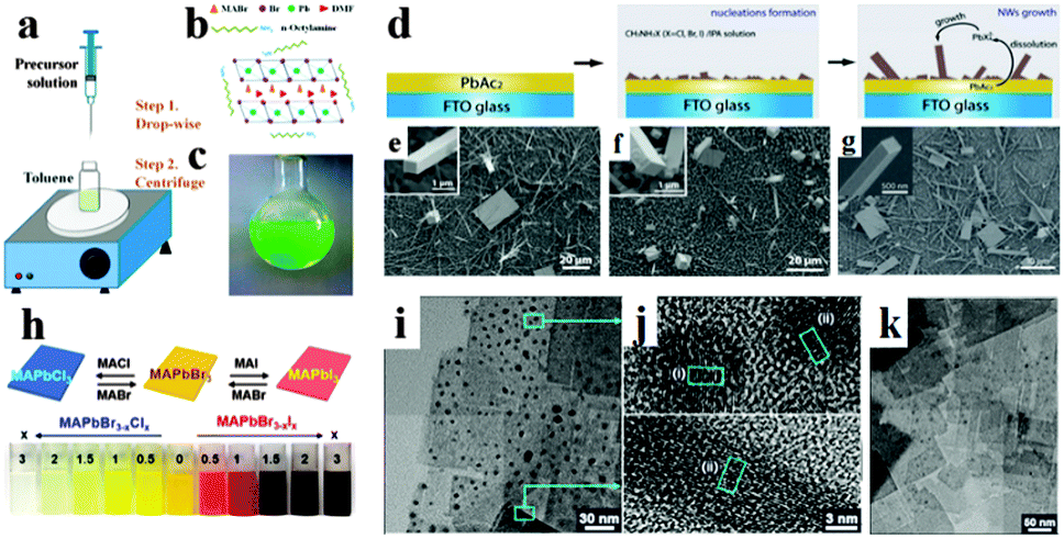 | ||
| Fig. 7 Synthesis of perovskite CH3NH3PbBr3 quantum dots. (a) Schematic illustration of the reaction system and process. (b) Illustration of starting materials. (c) Optical image of colloidal CH3NH3PbBr3 solution. Reproduced from ref. 43 with permission. Copyright 2015 American Chemical Society. Synthesis of single crystal perovskite CH3NH3PbX3 (X = Cl, Br or I) nanowires. (d) Schematic illustration of the nanowires growth process. SEM images of CH3NH3PbCl3 (e), CH3NH3PbBr3 (f) and CH3NH3PbI3 (g) nanostructures, the insets are the corresponding magnified view. Reproduced from ref. 26 with permission. Copyright 2015 Nature Publishing Group. Synthesis of perovskite CH3NH3PbX3 nanocrystals (NCs). (h) Illustration of the reversible anion exchange reaction. (i) HRTEM images of MAPbBr3 NCs. (j) Lattice-resolved images and intensity line profiles for the regions (i) and (ii) of the nanoplates. (k) HRTEM images of MAPbCl3. Reproduced from ref. 86 with permission. Copyright 2015 American Chemical Society. | ||
 | ||
| Fig. 8 Synthesis of two dimensional perovskite (C4H9NH3)2PbBr4 crystals. (a) Schematic of a single layer (C4H9NH3)2PbBr4 structure. (b) Optical image of the 2D square sheets perovskite. Scale bar is 10 mm. (c) AFM image and height profile of several single layer perovskites. (d) AFM image and height profile of a double layer perovskite. Reproduced from ref. 87 with permission. Copyright 2015 Science. | ||
In conclusion, the facile solution process techniques for preparing crystal perovskites MAPbX3 are highly efficient and applicable. However, the disadvantages such as uncontrollable morphology, low repeatability of crystal perovskites and pinholes in perovskites result from solution approaches inhibit the large-scale application. Therefore, developing more efficient and controllable methods for fabricating high quality crystal perovskites MAPbX3 is urgent.
3.2 Vapor evaporation methods
With the development of solution processed methods, vapor evaporation methods have also been employed for producing organometal halide perovskites. Compared to the solution approach, vapor evaporation methods tend to produce perovskites with high crystallinity but low yield. By employing in situ X-ray diffraction (XRD)89 for tracking the phase of perovskites (CH3NH3)Pb(I,Cl)3 formed with the vacuum-based coevaporation method, Pistor et al. observed a broad miscibility gap in-between different phases. Besides, they found that the composition of the resulting perovskites was strongly depended on the precursor flux ratios, and the synthesized CH3NH3PbI3 was conformed to be cubic rather than the usual tetragonal phase that exists at room temperature. Similar to the solution processed method, single-step and sequential step vapor evaporation methods were explored for synthesizing crystal perovskites.Thermal evaporation has been employed to fabricate perovskite films with better homogeneity and higher crystalline through either co-evaporation90 or single source evaporation91 early in the 1990s. The former technique requires the fine balance of the two source evaporation rates which is difficult due to the much higher vapor pressure of the organic component compared to the inorganic counterpart; whereas the latter needs dedicated equipment. Chen et al. synthesized polycrystalline perovskite thin film with full surface coverage, small surface roughness and grain size upto microscale by employing a low-temperature vapor-assisted solution process.92 Furthermore, Liu et al. fabricated compact and uniform flat films of mixed halide perovskite CH3NH3PbI3−xClx with low defect density by using a dual-source vapor deposition method.93
The chemical vapor deposition (CVD) method has been employed for fabricating low dimensional perovskite crystals as well. Via a two-step chemical vapor deposition (CVD) method, Xiong's group successfully synthesized free-standing CH3NH3PbI3 nanowires,94 CH3NH3PbI3 platelets95 and CH3NH3PbI3−aXa (X = Br, Cl) nanoplatelets.96Fig. 9a displays the synthesis setup using a vapor-transport system. Xiong et al. obtained a single crystal CH3NH3PbI3 nanowire with a length of upto 20 μm and width of ca. 500 nm (Fig. 9b) by converting PbI2 nanowires (which were first synthesized on silicon oxide substrates by CVD method at 380 °C) through a gas-solid hetero-phase reaction.94 Using a freshly cleaved muscovite mica substrate by a similar CVD method, they converted PbI2 platelets into CH3NH3PbI3 platelets through intercalation of CH3NH3I.95 As shown in Fig. 9c, the thickness of PbI2 and CH3NH3PbI3 platelets (before and after conversion) correlates with each other by a factor of 1.81 and the geometries of CH3NH3PbI3 preserve that of PbI2. By adjusting the conversion temperature and pressure of PbX2 platelets, they further synthesized CH3NH3PbI3−aXa nanoplatelets.96 The morphologies of lead halides are maintained after their conversion into perovskites exhibiting triangular or hexagonal platelets with a nanoscale thickness (10–300 nm) and an edge length of several to tens of micrometres (Fig. 9d).
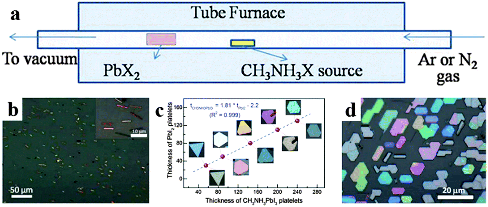 | ||
| Fig. 9 Illustration of two-step chemical vapor deposition for low dimensional perovskite single crystals. (a) Schematic of the synthesis setup. (b) SEM image of CH3NH3PbI3 nanowires. Insets is their corresponding SAED patterns. Reproduced from ref. 93 with permission. Copyright 2015 American Chemical Society. (c) Thickness of PbI2 platelets before and after being converted to CH3NH3PbI3. Reproduced from ref. 94 with permission. Copyright 2014 American Chemical Society. (d) Optical image of CH3NH3PbI3−aCla nanoplatelets. Reproduced from ref. 95 with permission. Copyright 2014 Wiely. | ||
4 Optoelectronic applications of crystal organometal halide perovskites
The dramatic increase of organometal halide perovskites in solar cells has aroused the interest of scientists across all over the world. The strong and intense PL, low non-radiative recombination rates and long carrier lifetime of pure and mixed-composition perovskites extend their applications into the optoelectronic field such as light-emitting diodes (LEDs), lasers and photodetectors. Organometal halide perovskites thus evoke new research interest in the optoelectronic field. Next, we will discuss the up to date research progress of perovskites in the optoelectronic field.4.1 Perovskite solar cells
Recently, many reports have focused on the organometal halide perovskite solar cells, describing the basic fundamentals of perovskite materials, device structure and fabrication for a better understanding of the high-efficiency perovskite solar cells.31,97–99 Integrating high efficiency, ease process procedure and low cost together, perovskite solar cells have shown great promise for practical applications. Solar cells employing perovskites as absorbents originated from the field of dye-sensitized solar cells (DSSCs).100 Organometal halide perovskite was first used as a sensitizer in liquid DSSCs in 2009, showing an efficiency of only 3.8% based on perovskite CH3NH3PbI3.101 Because perovskite easily dissolves and degrades in organic liquid electrolyte, initial perovskite solar cells were unstable. Real breakthrough were achieved following the exploitation of solid state hole transport materials in perovskite solar cells. By replacing the liquid electrolyte with solid hole conductor spiro-MeOTAD (2,2′,7,7′-tetrakis-x-2′,7,7′-tetrakis-9,9′-spirobifluorene)102 and poly-triarylamine63 in perovskite solar cells, enhanced power conversion efficiencies (PCE) of 9.7% and 12% were gained. Subsequently, Burschka et al. developed a sequential deposition method for the formation of perovskite within the porous metal oxide film, and achieved a higher efficiency of approximately 15% with increased reproducibility.67Fig. 10a depicts the schematic mesoporous perovskite solar cell configuration.31 And the vacuum energy levels for the corresponding component in solar cells are illustrated in Fig. 10b, which indicates the efficient separation of electrons and holes. Seen from Fig. 10c, the best-performing solar cell yields a high efficiency of 15%, with the open-circuit voltage (VOC), short-circuit current (JSC) and fill factor (FF) of 20.0 mA cm−2, 993 mV and 0.73.67 The sequential deposition technique for the fabrication of perovskite-sensitized mesoscopic solar cells could achieve both high efficiency and high stability which exhibit remarkable advantages over the previous single deposition technique. Furthermore, a combination of delicate interface engineering and metal co-doped spiro-OMeTAD enabled the fabrication of planar perovskite solar cells in air and from solution at low temperatures, yielding a robust PCE of 19.3%.15 A typical SEM image of the solar cell structure is shown in Fig. 10d. Differing from the common perovskite solar cell, ITO (indium tin oxide) modified with poly-ethyleneimine ethoxylated (PEIE) was used to reduce the work function. Besides, yttrium-doped TiO2 (Y-TiO2) was used as the electron transport layer (ETL) to enhance electron extraction and transport. As can be observed in Fig. 10e, the favourable energy match between the CBM (conduction band minimum) of Y-TiO2 and the HOMO (highest occupied molecular orbital) of spiro-OMeTAD with the CBM and VBM (valence band maximum) of the perovskites allows for efficient extraction of photogenerated carriers within perovskites. Seen from Fig. 10f, the optimized perovskite solar cell gains a PCE of 19.3% under AM 1.5 illumination without antireflective coating, with the VOC, JSC and FF of 1.13 V, 22.75 mA cm−2 and 0.75, respectively. Very recently, by replacing CH3NH3 of CH3NH3PbI3 by the FA analogue through an intramolecular exchange process, a certified record efficiency of 20.1% for the perovskite solar cell was proved.17 Developing novel approaches to increase the perovskite grain size and passivate surface defects is likely to be critical for further advancement of perovskite solar cells.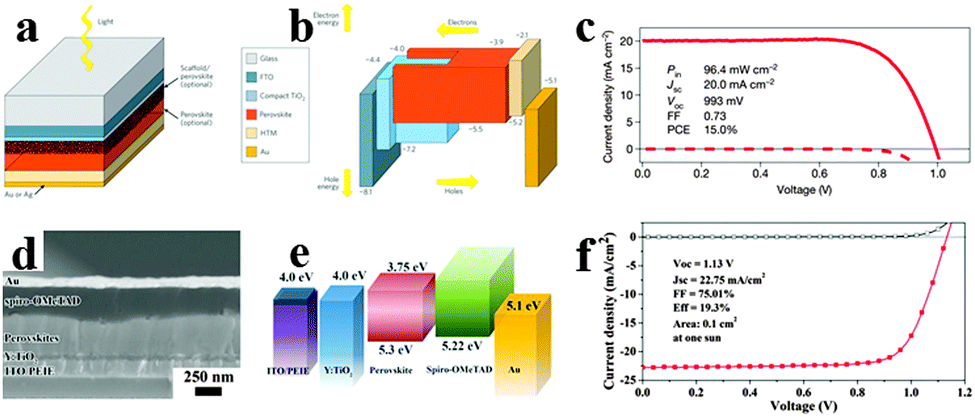 | ||
| Fig. 10 Mesoporous CH3NH3PbI3 based perovskite solar cell. (a) Mesoporous perovskite solar cell configuration. (b) Vacuum energy levels for corresponding component in solar cell. Reproduced from ref. 31 with permission. Copyright 2014 Nature Publishing Group. (c) J–V characteristics for a best-performing cell. Reproduced from ref. 67 with permission. Copyright 2013 Nature Publishing Group. Planar CH3NH3PbI3−xClx based perovskite solar cell. (d) SEM image of the planar perovskite solar cell. (e) Vacuum energy levels of each functional layer in the device. (f) J–V characteristics for the champion cell. Reproduced from ref. 15 with permission. Copyright 2014 Science. | ||
4.2 Light-emitting electrochemical cells
A light-emitting electrochemical cell (LEC) is a solid-state device that generates light from electric current. The LEC is composed of an organic semiconductor light active layer sandwiched between two metal electrodes. Pei et al. have developed a LEC by addition of an inorganic salt into a mixture of a conjugated luminescent polymer and an ionic conductive polymer in 1995.103 LECs emerged as a potential alternative to organic light-emitting diodes (OLEDs) owing to the use of air-stable injection layers and/or electrodes and simple device architecture.104,105 By replacing organic cation CH3NH3+ with FA+, organometal halide perovskite FAPbBr3 nanoparticles (NPs) were successfully synthesized and applied in LECs, exhibiting a stable luminance of around 1–2 cd m−2 at low driving currents.106Fig. 11a depicts the perovskite NP based LEC device. Seen from Fig. 11b, both MAPbBr3 and FAPbBr3 exhibit a near band edge emission with a narrow full width at the half-maximum of approximately 19 nm, indicating high crystallinity of the prepared NPs. Besides, exchange of MA to FA red-shifts the emission spectrum of perovskite nanoparticles from 532 to 545 nm. A stable luminance of 1–2 cd m−2 at low driving currents was achieved for FAPbBr3 materials (Fig. 11c). The report introduces us novel synthesis concept to fabricate FAPbBr3 NPs, and explores new application of organometal halide perovskites in the development of thin-film lighting devices.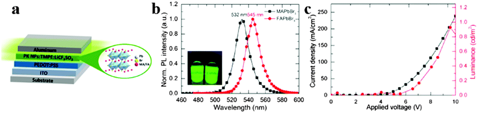 | ||
| Fig. 11 Hybrid lead halide perovskite nanoparticles based light-emitting electrochemical cells (LECs). (a) Device architecture of the perovskite LECs. (b) PL of MAPbBr3 and FAPbBr3 NPs in THF. Inset is the PL photograph of NPs in THF. (c) Luminance–current density versus applied voltage plot of FAPbBr3 based LECs. Reproduced from ref. 105 with permission. Copyright 2015 American Chemical Society. | ||
4.3 Light-emitting diodes (LEDs)
Light-emitting diodes (LEDs), a kind of solid-state lighting device based on inorganic semiconductors could provide highly efficient and convenient light point sources of different colours.107 The emergence of white LEDs is acquiring an increasing market share in ambient illumination, while challenges such as highly efficient light emission spanning the visible spectrum and exceptional colour quality at low cost still exist.108 Organometal halide perovskites have the potential to take these challenges, resulting from their extraordinary optical properties and compatibility with roll-to-roll solution-processed techniques.38,109Perovskite LEDs were first demonstrated in the 2000s in organometal halide perovskite with organic cations exhibiting layered two-dimensional structures.8 Recently, organometal halide perovskite aroused new research interest in light-emitting diodes.110–113 Tan et al. reported high-brightness light-emitting diodes based on solution-processed organometal halide perovskites CH3NH3PbI3−xClx, CH3NH3PbBr3 and CH3NH3PbI3−xBrx, and demonstrated electroluminescence in the near-infrared, green and red by tuning the halide compositions of perovskites at room temperature.114 The device structure of the green CH3NH3PbBr3 perovskite light-emitting diode (PrLED) is illustrated in Fig. 12a. CH3NH3PbBr3 and CH3NH3PbBr2I PrLEDs emit uniform green and red electroluminescence (Fig. 12b). Seen from Fig. 12c, perovskites with CH3NH3PbBr3, CH3NH3PbBr2I (mixed-bromide–iodide perovskite) and CH3NH3PbI3−xClx (mixed-chloride–iodide perovskite) compositions emit at green (517 nm) with a luminance of 364 cd m−2 and red (630 nm, 754 nm) wavelengths with an infrared radiance of 13.2 W sr−1 m−2. Furthermore, electroluminescence quantum efficiency of CH3NH3PbBr3 PrLED is proved to enhance with the increase of injection current density, which indicates a need for high charge densities to achieve efficient radiative recombination. To avoid the expensive, unstable and low-conductivity properties of fluorenes, Hoye et al. produced fluorene-free PrLEDs by employing the spatial atmospheric atomic layer deposition (SAALD) technique that enabled the deposition of ZnO films directly onto the CH3NH3PbBr3 perovskite, and achieved an improved turn-on voltage and higher luminance than those previously reported results using F8.115
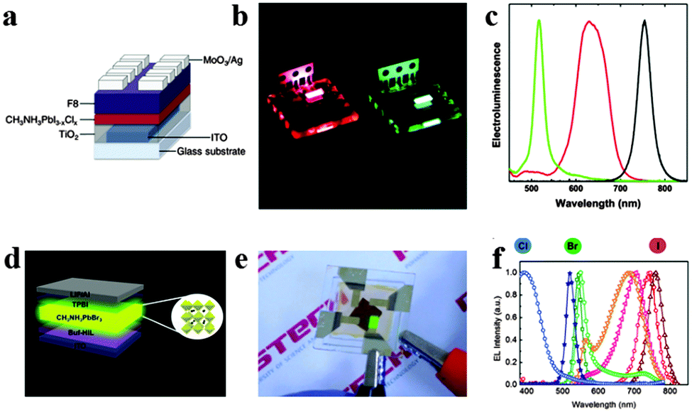 | ||
| Fig. 12 Bright light-emitting diodes (LEDs) based on perovskites. (a) Device architecture of the CH3NH3PbI3−xClx LED. (b) Photograph of the red and green PrLEDs. (c) EL of PrLEDs with varying halides. Reproduced from ref. 113 with permission. Copyright 2014 Nature Publishing Group. Multicolored perovskite light-emitting diodes (PrLED). (d) PrLED structure based on CH3NH3PbBr3. (e) Image of green-emitting PrLEDs. (f) EL of PrLEDs with CH3NH3PbClxBryI3−x−y. Reproduced from ref. 26 with permission. Copyright 2015 Wiley. | ||
With the development of PrLEDs, interface engineering has been proved to be an effective way for improving carrier transport.116,117 Satisfied emission performance has also been achieved in an inverted CH3NH3PbClxBryI3−x−y based LEDs structure by modifying the conventional PEDOT:PSS hole-injection layer with a perfluorinated polymeric acid.24 The schematic PrLED structure is displayed in Fig. 12d, in which Buf-HIL is composed of PEDOT:PSS and a perfluorinated polymeric acid (PFI). Fig. 12e shows the green emitting PrLEDs with high color purity. As can be observed in Fig. 12f, the wide tunability of the electroluminescence (EL) spectrum in CH3NH3PbClxBryI3−x−y based PrLEDs is successfully achieved by substitution of Br ions with I ions and Cl ions. Bright flexible perovskite LEDs (PrLEDs) with high spectral purity at room temperature and multicolored PrLEDs by substituting Br− with I− and Cl− (CH3NH3PbClxBryI3−x−y) were demonstrated. Much higher luminance, current efficiency (CE) and external quantum efficiency (EQE) (417 cd m−2, 0.577 cd A−1, 0.125%) values than the conventional LED were achieved. Multicolored PrLEDs with high luminance are successfully implemented in the report, which would facilitate the facile large-scale production of efficient flat-panels or flexible displays and solid-state lighting with high color purity. In conclusion, the selection of electrode contacts and transport layers with suitable conductivity and band alignment for efficient charge injection is great challenge, and minimizing series resistance from these layers is crucial since perovskite based LEDs operate at high current densities.
Along with the research progress of perovskite film based LEDs, low dimensional perovskites with specific morphologies are gaining increasing attention in LEDs recently. By using a low temperature anion exchange technique, a CH3NH3PbBr3 nanorod array was successfully converted to a CH3NH3PbI3 nanorod with preserved morphology, both of which exhibit room temperature EL at room temperature and the application of them in LEDs is further demonstrated.22
Organometal halide perovskite based LEDs with high color purity and facile synthesis provide us low-cost and high efficient semiconductor materials, which may further accelerate the progress of LEDs. In addition, low dimensional perovskites have demonstrated good performance in LEDs as well, which provide us a new horizon in broadening the investigation of perovskite materials for optoelectronic applications.
4.4 Lasing
Since the first laser implemented a powerful, coherent light source by stimulated emission processes in an optical medium,118 it has been exploited for wide applications in telecommunications, lighting, displays, medicine and optical physics. Since miniaturization of silicon logic elements has created a bottleneck in inter- and intra-chip communications, the integration of optical interconnects onto silicon chips has become crucial.119 However, material lattice mismatch and incompatible growth temperatures between a high performance III–V semiconductor and silicon have fundamentally restricted monolithic integration of lasers onto silicon substrates,120 which further inhibit the search for cost-effective, massively scalable and streamlined fabrication of on-chip light sources. Organometal halide perovskites fabricated by the room temperature solution process with excellent optical properties thus indicate promising application in lasing at room temperature.121Biexcitonic lasing has been observed in layered perovskite (C6H13NH3)2PbI4 below 40 K early in the 1990s.122 Recently, Xing et al. observed an ultra-stable amplified spontaneous emission at strikingly low thresholds of 12 ± 2 μJ cm−2 through examining the amplified spontaneous emission (ASE) behavior of solution-processed perovskites CH3NH3PbX3 in a cavity-free configuration.123Fig. 13a shows room temperature lasing from CH3NH3PbI3 film consisting of single crystals, of which an optical micrograph of the single crystal is inserted. Wide wavelength tunability of ASE in visible spectral range (390–790 nm) through halide substitution of CH3NH3PbIxClyBr3−x−y is successfully achieved (Fig. 13b). The emission intensity of the perovskite laser increases superlinearly above the threshold fluence of 12 ± 2 μJ m−2 (Fig. 13c). Besides, a near invariance of the ASE intensity with a standard deviation of 0.2% about the mean intensity for ∼26 h was observed, revealing excellent optical stability of these perovskite gain media. The above ultra-stable ASE at strikingly low thresholds was supposed to originate from large absorption coefficients, ultralow bulk defect densities and slow Auger recombination in single crystal CH3NH3PbI3 film. Furthermore, optically pumped lasing has also been demonstrated at room temperature in CH3NH3PbI3 based polygonal spherical resonators.121
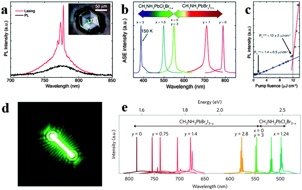 | ||
| Fig. 13 Perovskites for lasing. (a) CH3NH3PbI3 single crystal for lasing at room temperature. Inset is the optical micrograph. (b) Tunable ASE wavelengths from perovskite films. (c) PL intensity of CH3NH3PbI3 as a function of pump fluence. Reproduced from ref. 122 with permission. Copyright 2014 Nature Publishing Group. Lead halide perovskite nanowire lasers. (d) Lasing emission image of CH3NH3PbBr3. (e) Wide tunability of laser emission at room temperature. Reproduced from ref. 26 with permission. Copyright 2015 Nature Publishing Group. | ||
Compared to perovskite film, nanostructured perovskite laser with higher performance has been achieved.23,94 Zhu et al. reported solution processed single crystal lead halide perovskite nanowires CH3NH3PbX3 (X = CI, Br, Cl) lasing with low thresholds (220 nJ cm−2), high quality factors (Q ∼ 3600) and near-unity quantum yield.26 The emission image of a 13.6 μm CH3NH3PbBr3 NW above lasing thresholds is illustrated in Fig. 13d. Widely tunable lasing emission wavelengths covering the near-infrared (NIR) to the visible range at room temperature from single crystal nanowires of mixed lead halide perovskites are successfully implemented (Fig. 13e). The extraordinary lasing performance of lead halide perovskite nanowires was due to their long carrier lifetimes and low non-radiative recombination rates. Besides, Xing et al. demonstrated optical-pumped room-temperature visible and near-infrared solid-state nanowire lasers by employing free-standing perovskite nanowires CH3NH3PbI3, CH3NH3PbBr3 and CH3NH3PbIxCl3−x.94 Furthermore, Zhang et al. reported optically pumped lasing in polygonal nanocavities based on mixed halide perovskite CH3NH3PbI3−aXa (X = Br, Cl) nanoplatelets at room-temperature.96 The remarkable wavelength tunable whispering-gallery nanolasers can be easily integrated onto conductive platforms with a similar threshold of ∼40 μJ cm−2 and lasing peaks, suggesting the potential of integration onto optoelectronic chips. Liao et al. presented CH3NH3PbBr3 whispering-gallery mode WGM microdisk lasers (MDLs) and achieved single mode lasing with a threshold of 3.6 ± 0.5 μJ cm−2 and wavelength tunable lasing of perovskite WGM MDLs in the green range from 525 to 557 nm.78
Benefiting from large exciton binding energy and low defect density, organometal halide perovskites exhibit superior performance in laser. Single crystal nanowire perovskite lasing with a low threshold renovated laser field, which greatly promoted the development of low dimensional perovskite lasers. The superior lasing performance and wide tunability of emission colour across the visible spectrum, combined with the facile solution growth technique make lead halide perovskites excellent material for implementing nanostructured lasers in a wide range of applications, such as nanophotonics, optical computing and chemical/biological sensing.
4.5 Field-effect transistors (FETs)
Field-effect transistors (FETs) are consisted of p- or n-type semiconducting channel layers, with the conductivity modulated by applying a bias voltage to an adjacent insulated conducting gate. Alternative semiconducting materials with mobility comparable to that of amorphous silicon and low-cost process techniques124 are highly required to enable new opportunities of FETs for display and storage technologies. Organometal halide perovskites perfectly meeting the above demands therefore exhibited great potential in FETs.125Mitzi et al. have carried out intensive work on Tin(II)-based perovskite FETs and demonstrated high mobilities and Ion/Ioff ratios at the beginning of 2000s.126–128 By spin-coating thin film of organometal halide perovskite (C6H5C2H4NH3)2SnI4 to form the conducting channel, they achieved a field-effect mobility upto 0.62 cm2 V−1 s−1 and an Ion/Ioff ratio of above 104.127 Through substituting organic cations in hybrid perovskites for FETs, Mitzi et al. achieved a saturation-regime mobility as high as 1.4 cm2 V−1 s−1 and nearly an order of magnitude lower linear-regime mobility.127 Afterwards, they made further improvement through the melting processed deposition technique, where a saturation and a linear mobility of 2.6 and 1.7 cm2 V−1 s−1, and an Ion/Ioff of 106 were achieved.128
Chin et al. investigated the intrinsic charge transport parameters of CH3NH3PbI3via fabricating high-quality hybrid perovskite FETs, and found that screening effects associated with ionic transport can be effectively eliminated by lowering the operating temperature of FETs.129 The schematic of the bottom-gate, bottom contact FET configuration is shown in Fig. 14a. As can be observed in Fig. 14b, EL of CH3NH3PbI3 light emitting FET displays three peaks centred at 750 nm (Peak 1), 780 nm (Peak 2) and 800 nm (Peak 3) at the lowest temperature investigated (78 K), with distinct amplitudes and spectral positions at various temperatures. It is observed that Peak 1 and Peak 3 resulted from bound excitons in the low-temperature orthorhombic appear only below 158 K, while Peak 2 related to free excitons in the high temperature and a smaller bandgap tetragonal phase130 dominates the EL spectra at higher temperatures. Reducing the operating temperature turns out to be an effective way to reduce hysteresis effect due to ionic transport/screening, allowing us to record transport characteristics typical of conventional ambipolar semiconductor FETs (Fig. 14c and d). Typical p-type output characteristics are observed at 98 K and lower temperatures (Fig. 14d). Besides, the hysteresis of n- and p-type transfer characteristics of perovskite FET is substantially reduced below 198 and 98 K respectively, in accordance with the observation of ambipolar output characteristics.
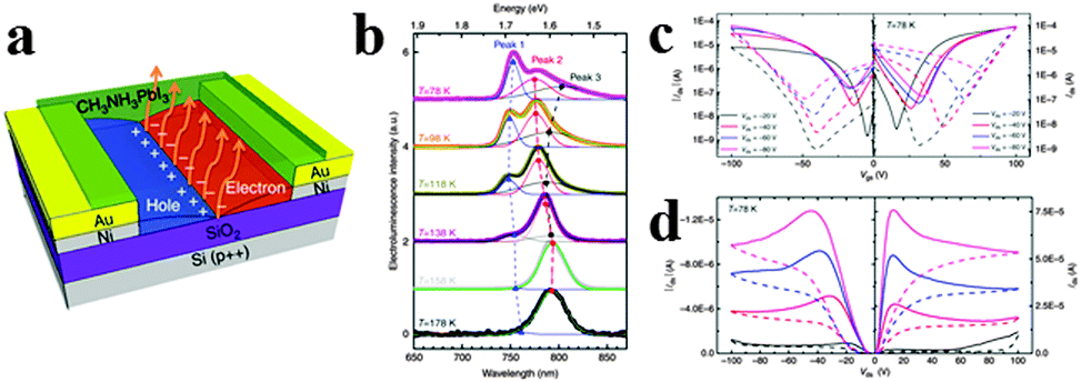 | ||
| Fig. 14 Lead iodide perovskite field-effect transistor (FET). (a) Schematic of the FET configuration. (b) Low-temperature EL of CH3NH3PbI3 FET. (c) Transfer and (d) output FET characteristics obtained at 78 K. Reproduced from ref. 128 with permission. Copyright 2015 Nature Publishing Group. | ||
The demonstration of organometal halide perovskite FETs paves the way to implement solution-processed perovskite light-emitting devices, and shows remarkable superiority over other conventional semiconductors. Furthermore, Sn and Pb based perovskite light-emitting field-effect transistors provide intrinsic transport parameters to guide the optimization of materials and solar cells, and will promote the development of novel electro-optic device concepts, such as gated light-emitting diodes and lasers operating at room temperature.
4.6 Photodetectors
Photodetectors that convert incident light into electrical signals are critical for a variety of industrial and scientific applications such as optical communications, environmental monitoring, day- and night-time surveillance and chemical/biological sensing.131,132 To achieve high performance photodetectors, exploiting semiconductor materials with high absorption extinction coefficient and large charge carrier mobility for ensuring sufficient light absorption and high photocurrent are emergent. Similar to GaAs, CH3NH3PbI3 possesses strong light absorption and activity of long-lived photocarriers for high-yield quantum conversion exhibited high photoconductive gain in photodetectors.133–135Xie et al. reported the first solution-processed organolead halide perovskite photodetector based on MAPbI3 film and flexible substrates, and gained a broad photoresponse range from 780 to 310 nm.136 The photoresponsivity and EQE of the MAPbI3 film-based flexible photodetectors achieved 3.49 A W−1 and 1.19 × 10³% at 365 nm, revealing high sensitivity, fast response speed and excellent stability. Subsequently, Dou et al. reported a solution-processed photodetector based on hybrid perovskite CH3NH3PbI3−xClx using an inverted device structure.25 The inverted device structure of the hybrid perovskite photodetector is displayed in Fig. 15a. Three types of devices were fabricated: PD1 without buffer, PD2 and PD3 with BCP (2,9-dimethyl-4,7-diphenyl-1,10-phenanthroline) and PFN (poly[(9,9-bis(3′-(N,N-dimethylamino)propyl)-2,7-fluorene)-alt-2,7-(9,9-dioctylfluorene)]) as cathode buffer layers, respectively. Seen from Fig. 15b, PD3 shows a significantly reduced Jd (dark current), a good rectification ratio of ∼105 (±1 V) and a very high detectivity of 8 × 10¹³ Jones at −100 mV. The marked increase in forward bias injection of PD3 was attributed to a formation of the dipole layer at the PCBM and Al interface which provides an extra electric field to prevent the hole injection while enhancing electron injection. The transient response results for the device with 0.01 cm2 area show a rise time of 180 ns and a decay time of 160 ns, while the rise time and decay time for a device with 0.1 cm2 area are both ∼600 ns (Fig. 15c). Besides, the quantum efficiency remains almost constant under different incident power densities, which suggests that a perovskite photodetector is well suited for detecting a wide range of incident powers. Subsequently, novel device structures for perovskite photodetectors emerged as a popular approach and turned out to be effective.137,138
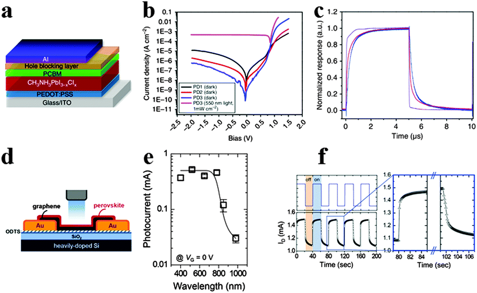 | ||
| Fig. 15 Solution-processed hybrid perovskite photodetectors. (a) Device structure of the hybrid perovskite photodetector. (b) Current density–voltage curves of photodetectors. (c) Transient photocurrent response. Reproduced from ref. 25 with permission. Copyright 2014 Nature Publishing Group. Perovskite-graphene hybrid photodetector. (d) Schematic diagram of the device. (e) Photocurrents of the hybrid photodetector as a function of the illumination wavelength. (f) Transient photocurrent response of the hybrid photodetector. Reproduced from ref. 144 with permission. Copyright 2015 Wiely. | ||
Following the development of a novel device structure, implementation of interface engineering emerged as an efficient technique for improving the performance of perovskite photodetectors as well.139,140 Dong et al. reported high gain solution-processed CH3NH3PbI3-based photodetectors with a broadband response ranging from the UV (ultraviolet) to the NIR by introducing 4,4′-bis[(p-trichlorosilylpropyl-phenyl)phenylamino]-biphenyl (TPD-Si2) as the hole transporting layer in a layered inverted structured photodetector.141 The photodetector yielded a very high gain of 405 ± 6 and a responsivity of 242 A W−1 at low bias (−1 V) that originated from hole traps caused by large concentration of Pb2+ in the perovskite film surface. Fang et al. reported a highly sensitive perovskite photodetector with low noise (16 fA Hz−1/2 at −0.1 V) via introducing device interface engineering and perovskite layer morphology improvement.142 The employment of interfacial electron transport layers (ETL) and hole transport layers (HTL), especially the trap passivation effect of the fullerene layer in device enables its direct measurement of light irradiance down to sub 1 pW cm−2.
With the explosive progress of an organometal halide perovskite film based photodetector, low dimensional perovskite of many active sites also aroused great interest in photodetectors.81,143 Zhuo et al. demonstrated porous CH3NH3PbBr3 nanowire visible-light photodetectors with a photoresponse time of only 0.12 s and a decay time of about 0.086 s.80 The high sensitivity and stability of porous CH3NH3PbBr3 nanowires were supposed to originate from the unique porous 1D geometry, many active sites and strong light absorption. Jang et al. designed plate-type NCs MAPbBr3−xClx and MAPbBr3−xIx NC photodetectors, and observed a strong correlation between the photocurrent and PL decay time.87 Among the mixed halide perovskites, I-rich composition MAPbBrI2 showed the highest photocurrent and the longest PL decay time, which could be ascribed to its pure tetragonal phase nature. First-principles density-functional theory calculations were employed to further understand the composition-dependent photoconversion efficiency.
To inhibit the rapid recombination of photo-induced electron–hole pairs in perovskite, perovskite hybrid photodetectors are gaining increasing attention.144 Lee et al. developed methylammonium lead halide/single-layer graphene hybridized photodetectors with photoresponse and a quantum efficiency of 180 A W−1 and 5 × 10⁴% at a relatively high illumination power of 1 μW.145Fig. 15d illustrates the structure of a CH3NH3PbI3 perovskite/graphene hybrid photodetector fabricated on a SiO2/Si substrate. Seen from Fig. 15e, a milliampere photocurrent was generated under illumination at wavelengths shorter than 800 nm, which is much higher than the pristine graphene photodetector. The broad spectral photo-responsivity between 800 and 400 nm was attributed to an increase in the optical absorption and photogating mechanisms of the hybrid photodetector. Based on the temporal response of the photocurrent, the rise and fall times of the perovskite-graphene hybrid photodetector were calculated to be 87 and 540 ms, indicating good on-off switching behaviour (Fig. 15f). Besides, the on-off switching behavior could maintain multiple cycles, suggesting the robustness and reproducibility of the perovskite/graphene hybrid photodetectors. Afterwards, Spina et al. designed a MAPbI3 nanowire/graphene hybrid photodetector, and gained a photoresponsivity as high as 2.6 × 10⁶ A W−1 that was four orders of magnitude higher than the above hybrid perovskite photodetector.146 The high device performance of a hybrid photodetector was mainly attributed to the nanowire perovskite morphology. The successful demonstration of graphene/perovskite hybrid photodetectors would encourage scientists to further investigate perovskite hybrid photodetectors.
Besides, there is a breakthrough in intrinsically narrowband photodetection with a widely tunable response range employing hybrid perovskite MAPbBr3−xClx and MAPbI3−xBrx single-crystal-based photodetectors recently.20Fig. 16a illustrates the structure of a single crystal perovskite photodetector. As seen in Fig. 16b, single crystal perovskites exhibit a single narrow peak close to the absorption edge of each kind of single crystal of different halide compositions, of which full-width at half-maximum is less than 20 nm, enabling narrowband photodetection. The narrowband photodetection was summarized to result from the surface-charge recombination-induced suppression of charge collection for short-wavelength excitation through a comparison of the device modelling results and EQE spectra. Furthermore, the response spectrum of a photodetector can be continuously modulated in the visible range from blue to red by adjusting the halide composition of solution processed single crystals. The 1.2 mm-thick MAPbBr3 single-crystal photodetector yields a stable photocurrent and dark current output (Fig. 16c). Fig. 16d records the temporal response with −4 V bias under 570 nm LED illumination with light intensities of 6 μW cm−2 and a modulation frequency of 150 Hz. In addition, the EQE spectra remained almost constant after prolonged exposure to air for both single-halide and mixed-halide perovskite single crystals, revealing better stability compared to their polycrystalline thin-film counterparts. This report provides us a novel design paradigm for a narrowband photodetector with low-cost and facile fabrication in broader applications where background noise emission needs to be suppressed.
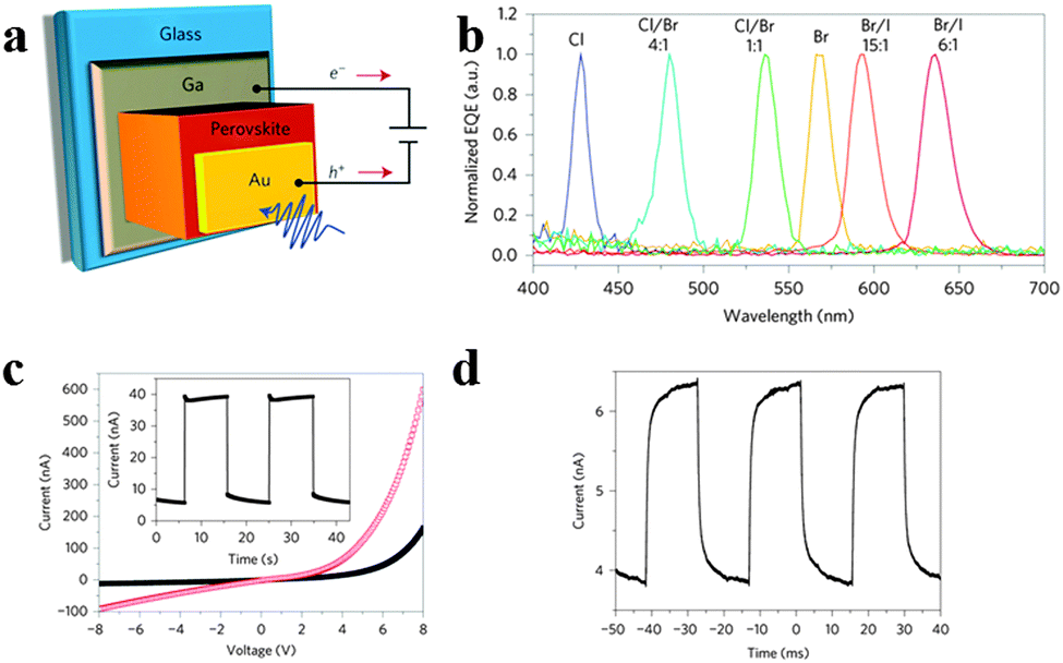 | ||
| Fig. 16 Narrowband perovskite photodetectors. (a) Device structure of the perovskite photodetector. (b) Normalized EQE spectra of the perovskite single crystal photodetectors. (c) Dark current and photocurrent of photodetector. Inset: repeated operation of the photodetector. (d) Temporal response. Reproduced from ref. 20 with permission. Copyright 2014 Nature Publishing Group. | ||
Unlike traditional inorganic semiconductors, the low-temperature solution process enables organometal halide perovskites to deposit on a broader range of substrate materials such as plastics, opening up opportunities to flexible electronic and photonic applications. Besides, the unique optoelectronic properties of perovskites lead to high detectivity and fast response that will greatly promote the research progress of perovskite photodetectors. Furthermore, the successful development of perovskite based hybrid photodetector provides us new horizon in exploring novel device configuration, which is expected to facilitate the development of imaging sensors suitable for low-light photography, UV detectors and smart skin sensors combined with other functionalities.
The remarkable optical properties and photophysical properties of organometal halide perovskites have opened up a multitude of optoelectronic applications beyond solar cells. Satisfied achievements have been obtained in perovskite optoelectronic devices, and the enthusiasm on them will be continually exciting in the future. Along with the successful development of three dimensional perovskites in optoelectronic applications, single crystal and low dimensional perovskites emerged and have demonstrated good performance. We believe that an enormous amount of research interest will be driven to the study of single crystal and low dimensional perovskites in light-emitting applications and optoelectronic devices, guiding a new avenue in perovskite research.
5 Conclusions and outlook
Organometal halide perovskite with extraordinary optoelectronic properties has astonished solar cell field with an unprecedented progress, and extended their potential into the optoelectronic field. In this focused review, we have summarized the recent research progress of crystalline organometal halide perovskite and their optoelectronic applications. Considering the achieved progress, organometal halide perovskites are supposed to be excellent candidates for solar cells, LEDs, laser, FETs and photodetectors with good performances. Persistent progress on organometal halide perovskites and their optoelectronic applications will definitely be continuously exciting and highly rewarding. Undoubtedly, there are still many challenges on the roads towards their practical integration into large scale production and application.Compared to conventional semiconductor-based solar cells, perovskite solar cells hold promise as a low-cost and high efficient alternative.15 However, almost all of the reported high efficiency perovskite solar cells are achieved on a small active area less than 0.1 cm2, since their energy conversion efficiencies decline quickly with the increased active areas. Therefore, how to fabricate perovskite solar cells with large areas and high quality is a great challenge. Although a much intrinsic phenomenon and mechanism has been explored in the recent research efforts, exciting research in searching new hybrid perovskites and revealing the unknown phenomenon and mechanism are still strongly expected.
The development of crystalline organometal halide perovskites and their optoelectronic applications are still in an early stage, there are many unanswered question left with regard to the synthesis, structure, function, etc. The high compatibility of perovskite structures in tailoring their halides, metal and organic cations provides strong support for in-depth investigation of structure–function relationships and further design of new perovskites. For example, mixed halide perovskites CH3NH3PbIxBr1−x or CH3NH3PbIxCl1−x exhibit better stability than that of CH3NH3PbI3. Besides, perovskites containing Pb show better stability and performance than that of Sn perovskites. In addition, nanostructured CH3NH3PbX3 perovskites show extreme instability under prolonged exposure to the electron beam in TEM and SEM. For low dimensional and single crystal perovskites, the synthesis is a long-term challenge in which the crystal nucleation and growth mechanism demands an intensive study. Besides, crystallographic structural and function analysis call for a comprehensive study as well. More precise control over morphology, composition and crystallization is required. Among all reported fabrication methods, the solution processed method takes obvious advantages in crystal quality and output, much more attention should be paid on the kinetics study. The development of a highly efficient and controllable synthesis technique will be helpful for in-depth investigation of the structure–function relationship. In return, understanding the structure–function relationship of perovskites would effectively guide the synthesis of new perovskites.
Although the study on utilization of perovskites in the optoelectronic field are growing fast in recent years, some key issues such as the basic concept of the p–i–n device structure and attributes of perovskites, especially the nature of heterojunctions and the origin of long lived charge carriers in perovskites are still ambiguous, which therefore need more scientific attention. Compared to the perovskite film contact issue in devices, single crystal and low dimensional perovskites with specific morphologies probably undergo a particular interfacial contact mechanism that require extra concern. Employing TiO2 as the compact layer has been proved to be an efficient way to reduce interface barrier potential, indicating an applicable approach for modifying the interface contact in perovskite optoelectronic devices. Development of a novel compact layer and a hole transfer layer with good performances is already under study, suggesting great promise in alleviating or removing the interfacial barrier. Recently, a perovskite/graphene hybrid optoelectronic device with inhibited carrier recombination has been successfully implemented, providing us a novel horizon in improving performance. In brief, fundamental studies on the photophysical properties, device concept and interfacial charge transfer dynamics should be strengthened for in-depth understanding their extraordinary performances and guiding the design of novel optoelectronic devices.
Lastly, to further accelerate the commercial progress of perovskite optoelectronic devices, stability issues of perovskites must be well addressed as soon as possible. Moisture and heat have been proved to be the main two factors causing the degradation of organometal halide perovskites. Besides, perovskites are unstable in the presence of many polar solvents because of their ionic crystal attributes. Essentially, understanding the degradation mechanisms of crystalline perovskite materials and searching for efficient approaches to hinder the serious degradation are key issues in the near future. Since the stability issue in perovskite solar cells has been improved by a porous carbon layer, thus it is natural to extend this strategy to other optoelectronic devices such as photodetectors to improve their stability. Besides, developing proper encapsulation techniques that keep out moisture, oxygen and ultraviolet radiation from perovskites could be an effective approach as well.
For optoelectronic devices, low fabrication cost and high device performance are the two critical indices for practical applications. Combining the facile solution processed method with excellent optoelectronic performance, organometal halide perovskites are elected as the best candidates among other routine semiconductors. Further study on exploring new technologies for higher reproducibility and stability of perovskites against heat and humidity is highly required, while higher performance is always the long-term challenge for the whole optoelectronic field.
Acknowledgements
J. Chen and S. Zhou contributed equally to this work. This work was supported by National Nature Science Foundation of China (21322106 and 51472097), and Ministry of Science and Technology of China (2015CB932600). The authors are indebted for the kind permission from the corresponding publishers/authors to reproduce their materials, especially figures, used in this article.Notes and references
- R. W. G. Wyckoff, Am. J. Sci., 1928, 16, 349–359 CrossRef CAS.
- J. Calabrese, N. L. Jones, R. L. Harlow, N. Herron, D. L. Thorn and Y. Wang, J. Am. Chem. Soc., 1991, 113, 2328–2330 CrossRef CAS.
- S. M. Wang, D. B. Mitzi, C. A. Field and A. Guloy, J. Am. Chem. Soc., 1995, 117, 5297–5302 CrossRef CAS.
- T. Ishihara, J. Takahashi and T. Goto, Phys. Rev. B: Condens. Matter Mater. Phys., 1990, 42, 11099–11107 CrossRef CAS.
- A. Poglitsch and D. Weber, J. Chem. Phys., 1987, 87, 6373–6378 CrossRef CAS.
- I. B. Koutselasy, L. Ducassez and G. C. Papavassiliou, J. Phys.: Condens. Matter, 1996, 8, 1217–1227 CrossRef.
- D. B. Mitzi, S. Wang, C. A. Feild, C. A. Chess and A. M. Guloy, Science, 1995, 267, 1473–1476 CrossRef CAS PubMed.
- D. B. Mitzi, K. Chondroudis and C. R. Kagan, IBM J. Res. Dev., 2001, 45, 29–45 CrossRef CAS.
- D. B. Mitzi, J. Solid State Chem., 1999, 145, 694–704 CrossRef CAS.
- D. B. Mitzi, Chem. Mater., 1996, 8, 791–800 CrossRef CAS.
- D. B. Mitzi, K. Chondroudis and C. R. Kagan, Inorg. Chem., 1999, 38, 6246–6256 CrossRef CAS PubMed.
- A. Kojima, K. Teshima, Y. Shirai and T. Miyasaka, J. Am. Chem. Soc., 2009, 131, 6050–6051 CrossRef CAS PubMed.
- M. M. Lee, J. Teuscher, T. Miyasaka, T. N. Murakami and H. J. Snaith, Science, 2012, 338, 643–647 CrossRef CAS PubMed.
- M. Liu, M. B. Johnston and H. J. Snaith, Nature, 2013, 501, 395–398 CrossRef CAS PubMed.
- H. Zhou, Q. Chen, G. Li, S. Luo, T. B. Song, H. S. Duan, Z. Hong, J. You, Y. Liu and Y. Yang, Science, 2014, 345, 542–546 CrossRef CAS PubMed.
- W. Nie, H. Tsai, R. Asadpour, J. C. Blancon, A. J. Neukirch, G. Gupta, J. J. Crochet, M. Chhowalla, S. Tretiak, M. A. Alam, H. Wang and A. D. Mohite, Science, 2015, 347, 522–525 CrossRef CAS PubMed.
- N. J. Jeon, J. H. Noh, W. S. Yang, Y. C. Kim, S. Ryu, J. Seo and S. I. Seok, Nature, 2015, 517, 476–480 CrossRef CAS PubMed.
- G. E. Eperon, S. D. Stranks, C. Menelaou, M. B. Johnston, L. M. Herz and H. J. Snaith, Energy Environ. Sci., 2014, 7, 982–988 CAS.
- G. Xing, N. Mathews, S. Sun, S. S. Lim, Y. M. Lam, M. Grätzel, S. Mhaisalkar and T. C. Sum, Science, 2013, 342, 344–347 CrossRef CAS PubMed.
- Y. J. Fang, Q. F. Dong, Y. C. Shao, Y. B. Yuan and J. S. Huang, Nat. Photonics, 2015, 9, 679–687 CrossRef CAS.
- Y. Li, X. Wang, S. Wu, H. Ci, H. Xu, X. Li, H. Sun, Z. Zhang, A. Cao, X. Guo and Y. Li, J. Mater. Chem. A, 2015, 3, 18847–18851 CAS.
- A. B. Wong, M. Lai, S. W. Eaton, Y. Yu, E. Lin, L. Dou, A. Fu and P. Yang, Nano Lett., 2015, 15, 5519–5524 CrossRef CAS PubMed.
- A. Fu and P. Yang, Nat. Mater., 2015, 14, 557–558 CrossRef CAS PubMed.
- Y. H. Kim, H. Cho, J. H. Heo, T. S. Kim, N. S. Myoung, C. L. Lee, S. H. Im and T. W. Lee, Adv. Mater., 2015, 27, 1248–1254 CrossRef CAS PubMed.
- L. Dou, Y. Yang, J. You, Z. Hong, W. H. Chang, G. Li and Y. Yang, Nat. Commun., 2014 DOI:10.1038/ncomms6404.
- H. M. Zhu, Y. P. Fu, F. Meng, X. X. Wu, Z. Z. Gong, Q. Ding, M. V. Gustafsson, M. T. Trinh, S. Jin and X.-Y. Zhu, Nat. Mater., 2015, 14, 636–643 CrossRef CAS PubMed.
- W. H. Zhang and B. Cai, Chin. Sci. Bull., 2014, 59, 2092–2101 CrossRef CAS.
- P. Gao, M. Grätzel and M. K. Nazeeruddin, Energy Environ. Sci., 2014, 7, 2448–2463 CAS.
- T. C. Sum and N. Mathews, Energy Environ. Sci., 2014, 7, 2518–2534 CAS.
- Q. Wang, H. J. Chen, G. Liu and L. Z. Wang, Sci. Bull., 2015, 60, 405–418 CrossRef CAS.
- M. A. Green, A. Ho-Baillie and H. J. Snaith, Nat. Photonics, 2014, 8, 506–514 CrossRef CAS.
- M. A. Pena and J. L. G. Fierro, Chem. Rev., 2001, 101, 1981–2017 CrossRef CAS PubMed.
- C. Li, X. Lu, W. Ding, L. Feng, Y. Gao and Z. Guo, Acta Crystallogr., 2008, 64, 702–707 CAS.
- A. Poglitsch and D. Weber, J. Chem. Phys., 1987, 87, 6373–6378 CrossRef CAS.
- N. Kitazawa, Y. Watanabe and Y. Nakamura, J. Mater. Sci., 2002, 37, 3585–3587 CrossRef CAS.
- Y. Y. Li, C. K. Lin, G. L. Zheng, Z. Y. Cheng, H. You, W. D. Wang and J. Lin, Chem. Mater., 2006, 18, 3463–3469 CrossRef CAS.
- H. P. Xu, J. Z. Sun, A. J. Qin, J. L. Hua, Z. Li, Y. Q. Dong, H. Xu, W. Z. Yuan, Y. G. Ma, M. Wang and B. Z. Tang, J. Phys. Chem. B, 2006, 110, 21701–21709 CrossRef CAS PubMed.
- W. J. Yin, T. T. Shi and Y. F. Yan, Adv. Mater., 2014, 26, 4653–4658 CrossRef CAS PubMed.
- G. E. Eperon, S. D. Stranks, C. Menelaou, M. B. Johnston, L. M. Herz and H. J. Snaith, Energy Environ. Sci., 2014, 7, 982–988 CAS.
- T. Ishihara, J. Takahashi and T. Goto, Solid State Commun., 1989, 69, 933–936 CrossRef CAS.
- G. C. Papavassiliou and I. R. Koutselas, Synth. Met., 1995, 71, 1713–1714 CrossRef CAS.
- C. C. Stoumpos, C. D. Malliakas and M. G. Kanatzidis, Inorg. Chem., 2013, 52, 9019–9038 CrossRef CAS PubMed.
- F. Zhang, H. Zhong, C. Chen, X. Wu, X. Hu, H. Huang, J. Han, B. Zou and Y. Dong, ACS Nano, 2015, 9, 4533–4542 CrossRef CAS PubMed.
- V. D. Innocenzo, G. Grancini, M. J. P. Alcocer, A. R. S. Kandadal, S. D. Stranks, M. M. Lee, G. Lanzani, H. J. Snaith and A. Petrozza, Nat. Commun., 2014, 5, 3586–3591 Search PubMed.
- A. Marchioro, J. Teuscher, D. Friedrich, M. Kunst, R. van de Krol, T. Moehl, M. Grätzel and J. E. Moser, Nat. Photonics, 2014, 8, 250–255 CrossRef CAS.
- V. Gonzalez-Pedro, E. J. Juarez-Perez, W. S. Arsyad, E. M. Barea, F. Fabregat-Santiago, I. Mora-Sero and J. Bisquert, Nano Lett., 2014, 14, 888–893 CrossRef CAS PubMed.
- E. J. Juarez-Perez, R. S. Sanchez, L. Badia, G. Garcia-Belmonte, Y. S. Kang, I. Mora-Sero and J. Bisquert, Chem. Lett., 2014, 5, 2390–2394 CAS.
- M. G. Ju, G. X. Sun, Y. Zhao and W. Z. Liang, Phys. Chem. Chem. Phys., 2015, 17, 17679–17687 RSC.
- F. Brivio, A. B. Walker and A. Walsh, APL Mater., 2013, 1, 0421111 Search PubMed.
- K. Yamada, T. Matsui, T. Tsuritani, T. Okuda and S. Ichiba, Z. Naturforsch., 1990, 45a, 307–319 Search PubMed.
- Q. Wang, Y. C. Shao, H. P. Xie, L. Lyu, X. L. Liu, Y. L. Gao and J. S. Huang, Appl. Phys. Lett., 2014, 105, 163508 CrossRef.
- Y. Takahashi, R. Obara, Z.-Z. Lin, Y. Takahashi, T. Naito, T. Inabe, S. Ishibashi and K. Terakura, Dalton Trans., 2011, 40, 5563–5568 RSC.
- K. Yamada, H. Kawaguchi, T. Matsui, T. Okuda and S. Ichiba, Bull. Chem. Soc. Jpn., 1990, 63, 2521–2525 CrossRef CAS.
- T. Y. Yang, G. Gregori, N. Pellet, M. Grätzel and J. Maier, Angew. Chem., 2015, 127, 8016–8021 CrossRef.
- O. Knop, R. E. Wasylishen, M. A. White, T. S. Cameron and M. J. V. Oort, Can. J. Chem., 1990, 68, 412 CrossRef CAS.
- E. J. Juarez-Perez, R. S. Sanchez, L. Badia, G. Garcia-Belmonte, Y. S. Kang, I. Mora-Sero and J. Bisquert, J. Phys. Chem. Lett., 2014, 5, 2390–2394 CrossRef CAS PubMed.
- D. Weber, Z. Naturforsch., 1978, 33b, 1443–1445 CAS.
- K. N. Liang, D. B. Mitzi and M. T. Prikas, Chem. Mater., 1998, 10, 403–411 CrossRef CAS.
- P. Qin, S. Tanaka, S. Ito, N. Tetreault, K. Manabe, H. Nishino, M. K. Nazeeruddin and M. Grätzel, Nat. Commun., 2014 DOI:10.1038/ncomms4834.
- A. Y. Mei, X. Li, L. F. Liu, Z. L. Ku, T. F. Liu, Y. G. Rong, M. Xu, M. Hu, J. Z. Chen, Y. Yang, M. Grätzel and H. W. Han, Science, 2014, 345, 295–298 CrossRef CAS PubMed.
- M. R. Leyden, L. K. Ono, S. R. Raga, Y. C. Kato, S. H. Wang and Y. B. Qi, J. Mater. Chem. A, 2014, 2, 18742–18745 CAS.
- J.-H. Im, C.-R. Lee, J.-W. Lee, S.-W. Park and N.-G. Park, Nanoscale, 2011, 3, 4088–4093 RSC.
- J. H. Heo, S. H. Im, J. H. Noh, T. N. Mandal, C.-S. Lim, J. A. Chang, Y. H. Lee, H.-J. Kim, A. Sarkar, M. K. Nazeeruddin, M. Gratzel and S. I. Seok, Nat. Photonics, 2013, 7, 486–491 CrossRef CAS.
- S. Colella, E. Mosconi, P. Fedeli, A. Listorti, F. Gazza, F. Orlandi, P. Ferro, T. Besagni, A. Rizzo, G. Calestani, G. Gigli, F. De Angelis and R. Mosca, Chem. Mater., 2013, 25, 4613–4618 CrossRef CAS.
- N. J. Jeon, J. H. Noh, Y. C. Kim, W. S. Yang, S. Ryu and S. I. Seok, Nat. Mater., 2014, 13, 897–903 CrossRef CAS PubMed.
- Z. G. Xiao, Q. F. Dong, C. Bi, Y. C. Shao, Y. B. Yuan and J. S. Huang, Adv. Mater., 2014, 26, 6503–6509 CrossRef CAS PubMed.
- J. Burschka, N. Pellet, S. J. Moon, R. Humphry-Baker, P. Gao, M. K. Nazeeruddin and M. Grätzel, Nature, 2013, 499, 316–320 CrossRef CAS PubMed.
- N. Pellet, P. Gao, G. Gregori, T.-Y. Yang, M. K. Nazeeruddin, J. Maier and M. Gratzel, Angew. Chem., Int. Ed., 2014, 53, 3151–3157 CrossRef CAS PubMed.
- Z. Song, S. C. Watthage, A. B. Phillips, B. L. Tompkins, R. J. Ellingson and M. J. Heben, Chem. Mater., 2015, 27, 4612–4619 CrossRef CAS.
- S. Colella, E. Mosconi, P. Fedeli, A. Listorti, F. Gazza, F. Orlandi, P. Ferro, T. Besagni, A. Rizzo, G. Calestani, G. Gigli, F. De Angelis and R. Mosca, Chem. Mater., 2013, 25, 4613–4618 CrossRef CAS.
- N. Yantara, F. Yanan, C. Shi, H. A. Dewi, P. P. Boix, S. G. Mhaisalkar and N. Mathews, Chem. Mater., 2015, 27, 2309–2314 CrossRef CAS.
- Y. Tidhar, E. Edri, H. Weissman, D. Zohar, G. Hodes, D. Cahen, B. Rybtchinski and S. Kirmayer, J. Am. Chem. Soc., 2014, 136, 13249–13256 CrossRef CAS PubMed.
- S. Yang, Y. Zheng, Y. Hou, X. Chen, Y. Chen, Y. Wang, H. Zhao and H. G. Yang, Chem. Mater., 2014, 26, 6705–6710 CrossRef CAS.
- T. Kollek, D. Gruber, J. Gehring, E. Zimmermann, L. Schmidt-Mende and S. Polarz, Angew. Chem., Int. Ed., 2015, 54, 1341–1346 CrossRef CAS PubMed.
- Y. C. Liu, Z. Yang, D. Cui, X. D. Ren, J. K. Sun, X. J. Liu, J. R. Zhang, Q. B. Wei, H. B. Fan, F. Y. Yu, X. Zhang, C. M. Zhao and S. Z. Liu, Adv. Mater., 2015, 27, 5176–5183 CrossRef CAS PubMed.
- Q. F. Dong, Y. J. Fang, Y. C. Shao, P. Mulligan, J. Qiu, L. Cao and J. S. Huang, Science, 2015, 347, 967–970 CrossRef CAS PubMed.
- D. Shi, V. Adinolfi, R. Comin, M. Yuan, E. Alarousu, A. Buin, Y. Chen, S. Hoogland, A. Rothenberger, K. Katsiev, Y. Losovyj, X. Zhang, P. A. Dowben, O. F. Mohammed, E. H. Sargent and O. M. Bakr, Science, 2015, 347, 519–522 CrossRef CAS PubMed.
- Q. Liao, K. Hu, H. Zhang, X. Wang, J. Yao and H. Fu, Adv. Mater., 2015, 27, 3405–3410 CrossRef CAS PubMed.
- M. I. Saidaminov, A. L. Abdelhady, B. Murali, E. Alarousu, V. M. Burlakov, W. Peng, I. Dursun, L. Wang, Y. He, G. Maculan, A. Goriely, T. Wu, O. F. Mohammed and O. M. Bakr, Nat. Commun., 2015 DOI:10.1038/ncomms8586.
- S. Zhuo, J. Zhang, Y. Shi, Y. Huang and B. Zhang, Angew. Chem., Int. Ed., 2015, 54, 5693–5696 CrossRef CAS PubMed.
- E. Horváth, M. Spina, Z. Szekrényes, K. Kamarás, R. Gaal, D. Gachet and L. Forró, Nano Lett., 2014, 14, 6761–6766 CrossRef PubMed.
- J. H. Im, J. Luo, M. Franckevičius, N. Pellet, P. Gao, T. Moehl, S. M. Zakeeruddin, M. K. Nazeeruddin, M. Grätzel and N. G. Park, Nano Lett., 2015, 15, 2120–2126 CrossRef CAS PubMed.
- L. C. Schmidt, A. Pertegás, S. González-Carrero, O. Malinkiewicz, S. Agouram, G. M. Espallargas, H. J. Bolink, R. E. Galian and J. Pérez-Prieto, J. Am. Chem. Soc., 2014, 136, 850–853 CrossRef CAS PubMed.
- J.-H. Im, C.-R. Lee, J.-W. Lee, S.-W. Park and N.-G. Park, Nanoscale, 2011, 3, 4088–4093 RSC.
- Y. Fu, F. Meng, M. B. Rowley, B. J. Thompson, M. J. Shearer, D. Ma, R. J. Hamers, J. C. Wright and S. Jin, J. Am. Chem. Soc., 2015, 137, 5810–5818 CrossRef CAS PubMed.
- W. M. Tian, C. Y. Zhao, J. Leng, R. R. Cui and S. Y. Jin, J. Am. Chem. Soc., 2015, 137, 12458–12461 CrossRef CAS PubMed.
- D. M. Jang, K. Park, D. H. Kim, J. Park, F. Shojaei, H. S. Kang, J. P. Ahn, J. W. Lee and J. K. Song, Nano Lett., 2015, 15, 5191–5199 CrossRef CAS PubMed.
- L. T. Dou, A. B. Wong, Y. Yu, M. L. Lai, N. Kornienko, S. W. Eaton, A. Fu, C. G. Bischak, J. Ma, T. Ding, N. S. Ginsberg, L.-W. Wang, A. P. Alivisatos and P. D. Yang, Science, 2015, 349, 1518–1521 CrossRef CAS PubMed.
- P. Pistor, J. Borchert, W. Fränzel, R. Csuk and R. Scheer, J. Phys. Chem. Lett., 2014, 5, 3308–3312 CrossRef CAS PubMed.
- M. Era, T. Hattori, T. Taira and T. Tsutsui, Chem. Mater., 1997, 9, 8–10 CrossRef CAS.
- D. B. Mitzi, M. T. Prikas and K. Chondroudis, Chem. Mater., 1999, 11, 542–544 CrossRef CAS.
- Q. Chen, H. Zhou, Z. Hong, S. Luo, H. S. Duan, H. H. Wang, Y. Liu, G. Li and Y. Yang, J. Am. Chem. Soc., 2014, 136, 622–625 CrossRef CAS PubMed.
- M. Liu, M. B. Johnston and H. J. Snaith, Nature, 2013, 501, 395–398 CrossRef CAS PubMed.
- J. Xing, X. Liu, Q. Zhang, S. T. Ha, Y. Yuan, C. Shen, T. C. Sum and Q. Xiong, Nano Lett., 2015, 15, 4571–4577 CrossRef CAS PubMed.
- S. T. Ha, X. Liu, Q. Zhang, D. Giovanni, T. C. Sum and Q. Xiong, Adv. Opt. Mater., 2014, 2, 838–844 CrossRef CAS.
- Q. Zhang, S. T. Ha, X. Liu, T. C. Sum and Q. Xiong, Nano Lett., 2014, 14, 5995–6001 CrossRef CAS PubMed.
- H. S. Jung and N.-G. Park, Small, 2015, 11, 10–25 CrossRef CAS PubMed.
- G. Hodes, Science, 2013, 342, 317–318 CrossRef CAS PubMed.
- S. D. Stranks and H. J. Snaith, Nat. Nanotechnol., 2015, 10, 391–402 CrossRef CAS PubMed.
- B. O'Regan and M. Grätzel, Nature, 1991, 353, 737–740 CrossRef.
- A. Kojima, K. Teshima, Y. Shirai and T. Miyasaka, J. Am. Chem. Soc., 2009, 131, 6050–6051 CrossRef CAS PubMed.
- H. S. Kim, C. R. Lee, J. H. Im, K. B. Lee, T. Moehl, A. Marchioro, S. J. Moon, R. Humphry-Baker, J.-H. Yum and M. Grätzel, Sci. Rep., 2012, 2, 1–7 Search PubMed.
- Q. Pei, G. Yu, C. Zhang, Y. Yang and A. J. Heeger, Science, 1995, 269, 1086–1088 CrossRef CAS PubMed.
- R. D. Costa, E. Ortí, H. J. Bolink, F. Monti, G. Accorsi and N. Armaroli, Angew. Chem., Int. Ed., 2012, 51, 8178–8211 CrossRef CAS PubMed.
- A. Sandström, A. Asadpoordarvish, J. Enevold and L. Edman, Adv. Mater., 2014, 26, 4974 CrossRef.
- M. F. Ayguler, M. D. Weber, B. M. D. Puscher, D. D. Medina, P. Docampo and R. D. Costa, J. Phys. Chem. C, 2015, 119, 12047–12054 Search PubMed.
- C. J. Humphreys, MRS Bull., 2008, 33, 459–470 CrossRef.
- M. H. Crawford, IEEE J. Sel. Top. Quantum Electron., 2009, 15, 1028–1040 CrossRef CAS.
- D. B. Mitzi, Prog. Inorg. Chem., 2007, 48, 1–121 CrossRef.
- N. K. Kumawat, A. Dey, K. L. Narasimhan and D. Kabra, ACS Photonics, 2015, 2, 349–354 CrossRef CAS.
- N. K. Kumawat, A. Dey, A. Kumar, S. P. Gopinathan, K. L. Narasimhan and D. Kabra, ACS Appl. Mater. Interfaces, 2015, 7, 13119–13124 CAS.
- O. A. Jaramillo-Quintero, R. S. Sanchez, M. Rincon and I. Mora-Sero, J. Phys. Chem. Lett., 2015, 6, 1883–1890 CrossRef CAS PubMed.
- G. Li, Z. K. Tan, D. Di, M. L. Lai, L. Jiang, J. H. W. Lim, R. H. Friend and N. C. Greenham, Nano Lett., 2015, 15, 2640–2644 CrossRef CAS PubMed.
- Z. K. Tan, R. S. Moghaddam, M. L. Lai, P. Docampo, R. Higler, F. Deschler, M. Price, A. Sadhanala, L. M. Pazos, D. Credgington, F. Hanusch, T. Bein, H. J. Snaith and R. H. Friend, Nat. Nanotechnol., 2014, 9, 687–692 CrossRef CAS PubMed.
- R. L. Z. Hoye, M. R. Chua, K. P. Musselman, G. Li, M. L. Lai, Z. K. Tan, N. C. Greenham, J. L. MacManus-Driscoll, R. H. Friend and D. Credgington, Adv. Mater., 2015, 27, 1414–1419 CrossRef CAS PubMed.
- L. Gil-Escrig, G. Longo, A. Pertegas, C. Roldan-Carmona, A. Soriano, M. Sessolo and H. J. Bolink, Chem. Commun., 2015, 51, 569–571 RSC.
- J. C. Yu, D. B. Kim, G. Baek, B. R. Lee, E. D. Jung, S. Lee, J. H. Chu, D. K. Lee, K. J. Choi, S. Cho and M. H. Song, Adv. Mater., 2015, 27, 3492–3500 CrossRef CAS PubMed.
- T. H. Maiman, Nature, 1960, 187, 493–494 CrossRef.
- D. A. B. Miller, Proc. IEEE, 2009, 97, 1166–1185 CrossRef CAS.
- M. Groenert, C. W. Leitz, A. Pitera, V. Yang, H. Lee and R. J. Ra, J. Appl. Phys., 2003, 93, 362–367 CrossRef CAS.
- B. R. Sutherland, S. Hoogland, M. M. Adachi, C. T. O. Wong and E. H. Sargent, ACS Nano, 2014, 8, 10947–10952 CrossRef CAS PubMed.
- T. Kondo, T. Azuma, T. Yuasa and R. Ito, Solid State Commun., 1998, 105, 253–255 CrossRef CAS.
- G. C. Xing, N. Mathews, S. S. Lim, N. Yantara, X. F. Liu, D. Sabba, M. Grätzel, S. Mhaisalkar and T. C. Sum, Nat. Mater., 2014, 13, 476–480 CrossRef CAS PubMed.
- D. B. Mitzi, J. Mater. Chem., 2004, 14, 2355–2365 RSC.
- C. R. Kagan, T. L. Breen and L. L. Kosbar, Appl. Phys. Lett., 2001, 79, 3536–3538 CrossRef CAS.
- C. R. Kagan, D. B. Mitzi and C. D. Dimitrakopoulos, Science, 1999, 286, 945–947 CrossRef CAS PubMed.
- D. B. Mitzi, C. D. Dimitrakopoulos and L. L. Kosbar, Chem. Mater., 2001, 13, 3728–3740 CrossRef CAS.
- D. B. Mitzi, C. D. Dimitrakopoulos, J. Rosner, D. R. Medeiros, Z. Xu and C. Noyan, Adv. Mater., 2002, 14, 1772–1776 CrossRef CAS.
- X. Y. Chin, D. Cortecchia, J. Yin, A. Bruno and C. Soci, Nat. Commun., 2015 DOI:10.1038/ncomms8383.
- H. H. Fang, R. Raissa, M. Abdu-Aguye, S. Adjokatse, G. R. Blake, J. Even and M. A. Loi, Adv. Funct. Mater., 2015, 25, 2378–2385 CrossRef CAS.
- J. J. Wang, F. F. Cao, L. Jiang, Y. G. Guo, W. P. Hu and L. J. Wan, J. Am. Chem. Soc., 2009, 131, 15602–15603 CrossRef CAS PubMed.
- H. Kind, H. Yan, B. Messer, M. Law and P. Yang, Adv. Mater., 2002, 14, 158–160 CrossRef CAS.
- H. R. Xia, J. Li, W. T. Sun and L. M. Peng, Chem. Commun., 2014, 50, 13695–13697 RSC.
- Y. Takahashi, H. Hasegawa, Y. Takahashi and T. Inabe, J. Solid State Chem., 2013, 205, 39–43 CrossRef CAS.
- Y. Guo, C. Liu, H. Tanaka and E. Nakamura, J. Phys. Chem. Lett., 2015, 6, 535–539 CrossRef CAS PubMed.
- X. Hu, X. Zhang, L. Liang, J. Bao, S. Li, W. Yang and Y. Xie, Adv. Funct. Mater., 2014, 24, 7373–7380 CrossRef CAS.
- H. W. Chen, N. Sakai, A. K. Jena, Y. Sanehira, M. Ikegami, K. C. Ho and T. Miyasaka, J. Phys. Chem. Lett., 2015, 6, 1773–1779 CrossRef CAS PubMed.
- D. Li, G. Dong, W. Li and L. Wang, Sci. Rep., 2014 DOI:10.1038/srep07902.
- C. Liu, K. Wang, C. Yi, X. Shi, P. Du, A. W. Smith, A. Karim and X. Gong, J. Mater. Chem. C, 2015, 3, 6600–6606 RSC.
- B. R. Sutherland, A. K. Johnston, A. H. Ip, J. Xu, V. Adinolfi, P. Kanjanaboos and E. H. Sargent, ACS Photonics, 2015, 2, 1117–1123 CrossRef CAS.
- R. Dong, Y. Fang, J. Chae, J. Dai, Z. Xiao, Q. Dong, Y. Yuan, A. Centrone, X. C. Zeng and J. Huang, Adv. Mater., 2015, 27, 1912–1918 CrossRef CAS PubMed.
- Y. J. Fang and J. S. Huang, Adv. Mater., 2015, 27, 2804–2810 CrossRef CAS PubMed.
- H. Deng, D. Dong, K. Qiao, L. Bu, B. Li, D. Yang, H. E. Wang, Y. Cheng, Z. Zhao, J. Tang and H. Song, Nanoscale, 2015, 7, 4163–4170 RSC.
- M. He, Y. Chen, H. Liu, J. Wang, X. Fang and Z. Liang, Chem. Commun., 2015, 51, 9659–9661 RSC.
- Y. Lee, J. Kwon, E. Hwang, C. H. Ra, W. J. Yoo, J. H. Ahn, J. H. Park and J. H. Cho, Adv. Mater., 2015, 27, 41–46 CrossRef CAS PubMed.
- M. Spina, M. Lehmann, B. Náfrádi, L. Bernard, E. Bonvin, R. Gaál, A. Magrez, L. Forró and E. Horváth, Small, 2015, 11, 4824–4828 CrossRef CAS PubMed.
| This journal is © The Royal Society of Chemistry 2016 |