 Open Access Article
Creative Commons Attribution 3.0 Unported Licence
Nanopatterned polymer brushes by reactive writing
Jonas F.
Nawroth
a,
Claudia
Neisser
b,
Artur
Erbe
b and
Rainer
Jordan
*a
aChair of Macromolecular Chemistry, School of Science, Technische Universität Dresden, Mommsenstr. 4, 01069 Dresden, Germany. E-mail: Rainer.Jordan@tu-dresden.de
bInstitute of Ion Beam Physics and Materials Research, Helmholtz-Zentrum Dresden-Rossendorf, 01328 Dresden, Germany
First published on 10th February 2016
Abstract
Polymer brush patterns were prepared by a combination of electron beam induced damage in self-assembled monolayers (SAMs), creating a stable carbonaceous deposit, and consecutive self-initiated photografting and photopolymerization (SIPGP). This newly applied technique, reactive writing (RW), is investigated with 1H,1H,2H,2H-perfluorooctyltriethoxysilane SAM (PF-SAM) on silicon oxide, which, when modified by RW, can be selectively functionalized by SIPGP. With the monomer N,N-dimethylaminoethyl methacrylate (DMAEMA), we demonstrate the straightforward formation of polymer brush gradients and single polymer lines of sub-100 nm lateral dimensions, with high contrast to the PF-SAM background. The lithography parameters acceleration voltage, irradiation dose, beam current and dwell time were systematically varied to identify the optimal conditions for the maximum conversion of the SAM into a carbonaceous deposit. The results of this approach were compared to patterns prepared by carbon templating (CT) under analogous conditions, revealing a dwell time dependency, which differs from earlier reports. This new technique expands the range of CT by giving the opportunity to not only vary the chemistry of the created polymer patterns with monomer choice but also vary the chemistry of the surrounding substrate.
Introduction
The modification of surfaces via polymer brushes is highly attractive to tailor the properties of interfaces. The fields of applications range from biotechnology to physics and materials science.1 While bringing preformed polymer chains into contact with a reactive surface (grafting-to) is a suitable approach,2 the polymerization from the surface has some distinct advantages over grafting-to, such as higher grafting density and higher layers.3For surface-initiated polymerizations (SIP), an initiator group has to be immobilized on the surface, which is routinely realized via self-assembled monolayers (SAMs). The SAM either already bears the initiating functionality or is modified in a post self-assembly step.4 In this manner, polymer brushes have been achieved by free5 and controlled radical,6 ring-opening metathesis7 and living cationic8 and living anionic polymerizations.9
It is not only possible to create uniform coverage of SAMs, and therefore also polymer brushes, but there are various ways to pattern a surface in the micro- and nanometer ranges.10–12 Patterning of polymer brushes provides exciting insights into numerous fields, e.g. in biology to study the basic principles in cell surface interactions.13
Anyhow, one has to be aware that patterned polymer brushes, especially nanometer-sized features, do not necessarily behave like their homogeneously grafted analogs. Simulations by Patra and Linse14 showed that brush heights universally scale with the size of the grafting area (footprint). Further, the outer parts of polymer brushes display different densities than the central part on top of the grafting area. To escape the osmotic pressure in the inner part of the grafting area, the brushes will extend over the latter. The amount of overlaying brushes depends on the ratio of the footprint (Δ) to the length of the polymer (N). With ratios Δ/N ≥ 4, the properties and lateral extension of the polymer brushes converge towards the values of homogeneously grafted brushes. However, the central part of a nanopatterned brush shows similar properties to homogeneously grafted brushes when a certain grafting density is reached. These simulations were confirmed by Lee et al.15 who investigated polymer features of 100–4000 nm size at different grafting densities and various polymerization times. It was found that the data from their AFM measurements fit the calculated scaling laws quite well.
Typically, patterning processes such as microcontact printing (μCP),16 nanoimprint lithography (NIL),17 scanning probe lithography,18,19 photolithography and electron beam lithography (EBL)20,21 are applied. Except for μCP, these techniques rely on the application of resists or a combination of resists, which often makes the patterning a multi-step process of local modification and development steps.
As opposed to this, Schmelmer et al.4 have shown that the formation of initiator patterns of nanometer size can be realized as resist-free. 4′-Nitro-1,1′-biphenyl-4-thiol (NBT) monolayers were directly irradiated by a focused electron beam, leading to crosslinking of the aromatic SAM and the chemical reduction of the terminal nitro group. The resulting areas of cross-linked 4′-amino-1,1′-biphenyl-4-thiol (cAMBT) were converted to 4′-azomethylmalonodinitrile-1,1′-biphenyl-4-thiol, which acted in a consecutive step as an initiator for free radical polymerization (FRP). This process of electron beam chemical lithography (EBCL) not only leads to more stable monolayers, due to the cross-linking, but also to a high chemical contrast via the modified end group. Later, Steenackers et al.22 showed that FRP from cAMBT can also proceed without further modification of the amino group, by using self-initiated photografting and photopolymerization (SIPGP). SIPGP is an initiator free polymerization that requires UV-irradiation and abstractable protons at the surface, and was shown to be suitable for acrylic, methacrylic as well as styrenic monomers.23,24 UV light excites the π-electrons of the monomer to an excited singlet state that translates to a triplet state via inter system crossing. This triplet state is in an equilibrium with a biradical form of the monomer's double bond and the latter is capable of abstracting protons from the surface, generating a surface bound radical.25 Earlier reports suggest that abstractable groups with bond dissociation energies (BDEs) below 100 kcal mol−1 (418 kJ mol−1)26,27 are necessary to take part in this process.
SIPGP circumvents the lengthy introduction of suitable initiator functionalities and provides the ability to create a sharp chemical contrast for the formation of patterned brush surfaces if there is a sufficient difference for the BDEs.
Steenackers et al.26 studied yet another approach of EBL to further investigate the potential of SIPGP. Electron beam induced carbon deposition (EBICD), usually an unwanted byproduct of every electron microscopy experiment, can also serve as an initiating surface pattern. Residual hydrocarbons from the surface or the chamber vacuum are reduced on the surface under the irradiation of the beam. The carbonaceous deposit mainly consists of sp2-carbon and roughly 10% sp3-carbon species and forms on a variety of surfaces, such as Si, GaAs, nanocrystalline diamond or glass.28 The C–H BDEs for sp3-carbon of polycyclic sp2-hydrocarbon precursors range from 80 to 301 kJ mol−1,29 so this method allows a direct patterning of surfaces and consecutive one-step SIPGP. With this method of carbon templating (CT), they were able to control the density of the EBICD by the applied electron dose. This was shown in experiments where dose gradients were written on surfaces. However, under the investigated conditions, the deposit itself is usually roughly 1 nm in height; a detailed characterization by AFM is difficult, because of the low physical and topographical contrast of the EBICD to the surrounding surface. Nevertheless, conclusions about the quality of the EBICD can be drawn from the consecutive SIPGP. Because polymer brushes will stretch out with increasing grafting density, the quality of the underlying pattern will display as a height function of the polymer layer.26 The measured height of the polymer brush pattern therefore can be controlled by the density of the deposit, if the SIPGP polymerization time (tP) is kept constant.
To fine tune the chemical contrast on the surface even further, one can also think about changing the chemistry of the non-irradiated area. A very common procedure is, as already stated, to cover the surface with SAMs. However, there is a major drawback for SAM modification in the CT approach, the insufficient coverage. Usually, for oxide surfaces, prior to the self-assembly process, the surface is cleaned from residual organic impurities by either plasma or piranha treatment. This results in a clean, homogeneous substrate and additionally in an increase of hydroxyl groups on the SiO2 surface. A maximum amount of OH-groups eventually leads to the most densely packed silane SAM. Unfortunately, either of these treatments would also remove the EBICD. In contrast, a subsequent silanization would not cover the surface with maximum density because on the one hand, the density of hydroxyl groups is lower and on the other hand, the area around the initiator footprint is occupied by polymer brushes trying to wet the surface. Silanizing between EBCID and SIPGP could also be complicated, since common alkylsilanes used for hydrophobization, e.g. dichlorodimethylsilane, would also serve as an initiator for SIPGP due to the low BDE, similar to the EBICD.
In contrast, SAMs from 1H,1H,2H,2H-perfluorooctyltriethoxysilane (PF-SAM) display CF2 or CF3 groups at the interface and high BDEs of F3C–F and H3C–F with 523 kJ mol−1 and 450 kJ mol−1,30 respectively, suggest that no surface bound radical will be formed under SIPGP conditions. Moreover, SAMs have been intensively investigated as EBL resists by Seshadri et al.31 They irradiated an uniformly covered octadecylsilane (ODS) surface with a focused electron beam and did a variety of analyses. AFM measurements showed a height decrease in the irradiated areas that referred to a partial degradation rather than a complete ablation. The necessary electron dose for the maximum height decrease was found to be 0.5 mC cm−2 after which the degradation leveled off and reached a plateau. Further, XPS and IR spectra revealed a decrease in the carbon and hydrogen contents in the irradiated ODS SAM, with an increasing amount of polar groups and cross-linking monolayers. The final residue was a stable carbonaceous film with a 30–40% loss of carbon and hydrogen, in comparison with the non-irradiated ODS layer.
Our hypothesis is that the PF-SAM, which should be unreactive under SIPGP conditions, due to its high BDEs, can be converted to a carbonaceous deposit by electron beam induced damage. We describe here this technique as reactive writing (RW) and compare it to the CT approach.
Results and discussion
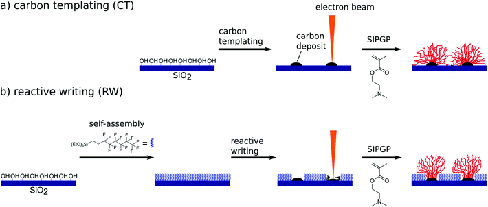
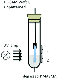
Scheme 1 shows the patterning process for the two applied methods of carbon templating (CT) and reactive writing (RW) of 1H,1H,2H,2H-perfluorooctyl self-assembled monolayers (PF-SAM) on SiO2 wafers. CT was performed as described in the literature.18 Briefly, under electron beam irradiation, carbon deposit is written directly onto the cleaned, unfunctionalized wafer surface. The substrate is immersed in the bulk monomer and under UV irradiation DMAEMA is selectively polymerized in the patterned areas. In the case of RW, the oxide surface is activated by air plasma treatment, prior to PF-SAM formation. The homogeneous PF-SAM is then degraded under electron beam irradiation, resulting also in carbonaceous residues. The consecutive SIPGP of DMAEMA again affects only the patterned areas. For better comparison, the identical layouts and conditions are investigated for both methods. The resulting polymer structures are analyzed by AFM under dry and ambient conditions in the tapping mode.To first test our assumption that the chosen PF-SAM is inaccessible towards surface grafting under SIPGP conditions, a model reaction is carried out. The setup is shown in Fig. 1.
The unpatterned, homogeneously covered PF-SAM wafer is partially immersed in the degassed bulk monomer and irradiated by UV light for 2 h. After excessive cleaning of the substrate with ethanol and MilliQ water as well as extensive ultrasonication in both solvents, ellipsometry measurements did not show any increase in layer thickness, neither in comparison with the same area before and after irradiation nor in comparison between the areas 1 and 2. To further quantify this result, XPS spectra of the areas 1 and 2 as well as a separate control sample were measured. The control sample was a 3-aminopropylsilane (APS) SAM on SiO2, with SIPGP-grafted PDMAEMA brushes on the APS layer. The N 1s signal at 402.6 eV that would arise from PDMAEMA was integrated for areas 1 and 2 and the control sample to 0.3%, 0.7% and 6.6%, respectively. The rise of 0.4% in the N 1s signal from 1 to 2 could be assigned to either a residual physisorbed DMAEMA or a measurement inaccuracy. However, the value is almost 10-fold smaller than the control and therefore we conclude that no polymerization takes place in non-irradiated areas of the PF-SAM.
Since the first assumption was validated, the second assumption that electron beam irradiation of PF-SAM results in a carbonaceous deposit was investigated. Therefore, rectangular (50 × 10 μm2) electron dose gradients ranging from 0–100 mC cm−2, 0–50 mC cm−2 and 0–10 mC cm−2 are created via RW, as well as CT to compare both techniques. Each gradient is the result of 100 stripes of 0.5 × 10 μm2 size of linearly increasing dose and each set of dose gradients is created at four different acceleration voltages of 2 kV, 5 kV, 10 kV and 20 kV. This results in a total of 12 gradients for RW and 12 for CT. It is noteworthy that these 12 gradients are on one single substrate, to minimize variations in the reaction parameters.
However, the investigation of the structures after the writing process is challenging, due to low height differences and low physical contrast between irradiated and non-irradiated areas. Therefore we estimate the quality of the carbon deposit from the consecutive SIPGP. As known from the literature, surface bound polymer brushes will stretch out as the grafting density increases. The polymer grafting density in SIPGP can be influenced by the irradiation time and thus, time of polymerization (tP). Due to the free radical mechanism of SIPGP, the polymer chain length is not significantly varied by tP,32 but the increasing brush grafting density leads to thicker polymer brush layers. Thus, if the polymerization parameters and dimensions of the pattern are otherwise unchanged, a higher polymer brush layer is the result of a higher initiator/grafting point density on the surface. In our case the initiator functionality is simply an abstractable surface function in the carbon deposit.
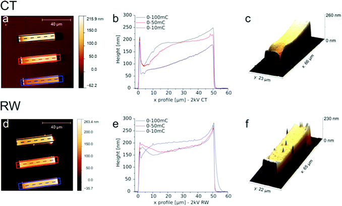
Fig. 2 shows exemplary AFM height scans and the corresponding height profiles from the gradients written at a 2 kV acceleration voltage for CT and RW, as well as a 3D representation of each 0–100 mC cm−2 gradient. With 2 h the tP was identical to the one in our first model reaction (Fig. 1). One can clearly see the amplification of the irradiated and the absence of polymer growth in the non-irradiated areas. The polymer brushes appear higher with increasing electron dose, suggesting a denser deposit beneath. A plateau in a polymer brush height of about 200 nm is reached at around 50 mC cm−2 for CT. These findings are in good agreement with the previous studies and seem to be independent of monomer choice.22 Furthermore, we see buckling at the edges of the polymer brush gradients, which is probably due to the preferred interactions of the polymer brushes with each other, compared to the surrounding area and therefore differ from the region within the polymer brush pattern. In the case of the RW, the brush height seems to be less dependent on the applied dose. A plateau can be seen at 2 mC cm−2, while doses above 10 mC cm−2 seem to have a lowering effect. Additionally, we see unexpected high polymer brushes at the low energy dose end of each gradient for both methods that we cannot explain to date.
In Fig. 3 the height profiles of the polymer brush gradients are displayed in dependency of the acceleration voltage for both techniques. Under the very same polymerization conditions, features of equal doses but written with lower acceleration voltages result, after SIPGP, in higher polymer brush patterns. Therefore, one can achieve a denser carbon deposit. This trend is observed for either method and can be explained by a higher surface sensitivity with lower beam energies, due to a smaller penetration depth. The plateau region, where the brush height does not grow further with increasing dose, is not reached in all cases. For CT, as already shown in Fig. 2, this value is achieved at 50 mC cm−2 at 2 kV, and shifts to 80 mC cm−2 for 5 kV and cannot be seen at higher voltages. There is, however, an unusual behavior at 5 kV, where the same dose in the 0–50 mC cm−2 range results in bigger polymer brush heights than for 0–100 mC cm−2. The origin of this is unclear. For RW the brush height seems to be less dependent on the applied electron dose. Again we can see that the plateau height shifts towards higher doses with increasing voltages, but the maximum height is reached in all four variations. The brush heights of around 200 nm in the plateau region are comparable in both methods showing a similar behavior and good reproducibility of carbonaceous species.
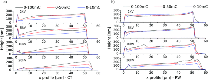 | ||
| Fig. 3 AFM height profiles of the polymer brush gradient cross sections analogous to Fig. 2 as a function of the irradiation dose 0–100 (black), 0–50 (red) and 0–10 mC cm−2 (blue) at different acceleration voltages (2, 5,10 and 20 kV) for (a) CT and (b) RW, tP = 2 h. | ||
As is known from the literature,33 the energy needed to dissociate hydrocarbons is only a few eV, therefore all applied conditions from 2 kV to 20 kV are more than sufficient to create contamination. In the case of CT, earlier experiments by Amman et al.34 showed that the growth rate of the deposit from residual carbon precursors is mostly diffusion limited. Plotting the height over the dose then might not lead to the right conclusions. Considering the writing parameters, the gradients not only vary in acceleration voltages but also vary in the beam currents, with larger currents for higher voltages (Table 1). If we now consider
 | (1) |
| Acceleration voltage | 2 kV | 5 kV | 10 kV | 20 kV |
|---|---|---|---|---|
| Current [pA] | 28 | 44 | 73 | 120 |
| Factor dwell time | 4.24 | 2.72 | 1.63 | 1 |
Fig. 4 shows the new correlation of the polymer brush height with the dwell time and the assumption of a time dependency for CT is confirmed. RW seems to be less dependent on the dwell time. The same dwell time for RW results in higher brushes and earlier plateaus compared to CT. This is most likely because of differences in precursor reservoir densities.
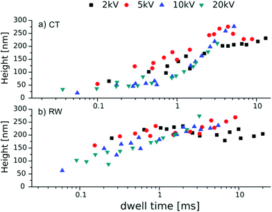 | ||
| Fig. 4 Polymer brush heights in dependency of the dwell time and the different acceleration voltages, for the electron dose gradients created by (a) CT and (b) RW, tP = 2 h. | ||
There are two different growth regimes for the electron-induced deposit. One is limited by the current density and independent of the precursor flux (electron limited regime – e.l.), and the other is limited by the flux and independent of the current density (precursor limited regime – p.l.). It is known from the literature that carbon precursors, as in our cases, fall into the p.l. regime.35 However, we do not have a gas flux for our precursors but a steady reservoir throughout irradiation. The only difference between RW and CT then is the precursor density. For RW a large amount of precursors (PF-SAM) covers the surface while for CT hydrocarbons are loosely spread over the surface. The incoming electron beam dissociates these and leads to depletion of precursors in this area. The higher mobility and the bigger concentration gradient of precursor molecules lead to surface diffusion towards the beam.35 Therefore we assume that although the CT curve appears sigmoidal and the RW curve looks asymptotic, the deposit growth mechanism is similar. The difference in dwell time dependency that can be observed in Fig. 4 is then a result of the shifted slope.
However, the trend within one method and varying acceleration voltages is less definite. The differences in the polymer brush height are less consistent, but there is a slight increase with decreasing voltage. A possible explanation could be drawn from the interaction characteristic of electron beams with solid substrates.
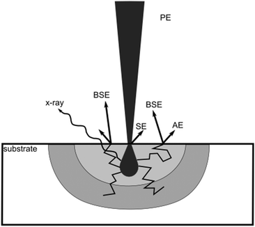
Fig. 5 shows a schematic of an electron beam scattering volume in an arbitrary substrate. The incoming primary beam does not exclusively realize the irradiation, but secondary electrons (SE) from the substrate or back-scattered electrons (BSE) increase the illuminated area. The amount and energy of SE and BSE increase with the acceleration voltage, which could be the reason for the decreased polymer brush heights at similar dwell times. However, 2 and 5 kV as well as 10 and 20 kV seem to be very similar to each other.
The amount of SE and BSE should not only be taken into consideration when it comes to the surface sensitivity of the primary beam, but as shown in Fig. 5, these electrons lead to wider structures in comparison with the areas which are covered by the primary beam. This results in parasitic carbon deposit growth or, for RW, degradation around the irradiation spot. Moreover, it is also well known that the amplification of surface patterns by polymer brushes leads to the widening of the resulting polymer feature.7 The chain length of the tethered polymer brush limits the maximum widening of a surface structure. Therefore it can only be the initiator footprint size plus twice the brush length or less, depending on the chemical nature of the brush and the surface and the resulting wetting effects. The relative widening should be less pronounced, the wider the footprint of the original pattern is, compared to the polymer chain length. The dimensions of the investigated dose gradients are 50 × 10 μm2, while the brush height in the plateau region indicated a length of roughly 200 nm. If the feature is written without parasitic irradiation, the width of the rectangles should not exceed 10.40 μm. Fig. 6 shows the width variation of the structure with the corresponding dwell time. The height profiles are measured along the y-axis, orthogonal to the profiles shown in Fig. 3. The data points are the result of five cross sections per acceleration voltage and dose gradient and are correlated to the corresponding dwell time in that part of the gradient.
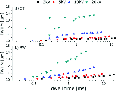 | ||
| Fig. 6 Width of the 50 × 10 μm2 polymer brush gradients prepared from electron dose gradients as a function of the dwell time by (a) CT and (b) RW, tP = 2 h. | ||
Two trends can be observed for CT and RW. On the one hand, the width of the polymer structure increases with increasing dwell time and on the other hand, it also increases for higher acceleration voltages. This is the result of increasing penetration depth and therefore increasing SE and BSE yield. These lead to unwanted irradiation and widening of the intended structure,35 which eventually also leads to polymerization in these areas.
The conclusion from these experiments is to use an electron beam of lower energy and to apply only small doses to the irradiated areas, which is controlled by the dwell time. This should result in narrow, yet dense carbon patterns for both methods.
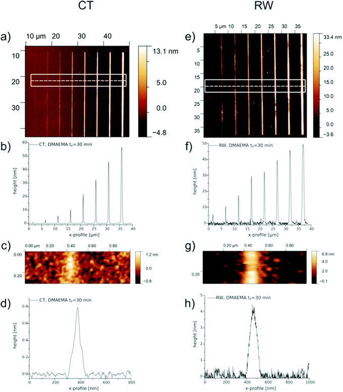
To optimize the lateral resolution and minimize the lateral feature size of RW, a line array is written with 2 kV, 21 pA, 0.8 μs dwell time, 0.5 mC cm−2 and 2 nm beam diameter. The same conditions are also applied for CT to compare both methods. The AFM scans of these patterns are displayed in Fig. 7. DMAEMA was polymerized for 30 min to yield lower brush grafting densities and therefore smaller lateral dimensions. Due to higher crowding of the brushes, the height scales with larger footprints, as it was already shown by Lee et al.,7 could also be observed in our experiments.
The height profiles determined from the AFM scans in Fig. 7 are fitted with a Gaussian curve to analyze the width of the single line features. The determined full width at half maximum (FWHM) are summarized in Table 2. Because of the issues of resolving the carbonaceous species prior to polymerization, the footprint of the structures is stated as the nominal width from the patterning software. However, it is possible for both methods to create polymer patterns with sub 100 nm dimensions. For the CT method, the minimal lateral dimension was determined to be 64 nm and therefore narrower as the feature at the same nominal footprint with RW. It is noteworthy that this could be realized at roughly a fifth of the brush height of RW, which directly translates into a lower grafting density for CT. From the values in Table 2 we can conclude that for low polymer brush heights CT and RW are comparable in their lateral dimension. At brush heights of about 30 nm, CT results in smaller widths than RW. This is probably due to the longer electron irradiation times needed to write larger features. The total amount of SE and BSE increases and the effect of carbon deposit conversion on a surface with higher precursor coverage would be more pronounced. It is noteworthy that polymer patterns with heights below 10 nm are of lower grafting density and are thus most likely not in the brush, but in the mushroom regime.
A comparison of the lateral dimensions to earlier studies has to be seen critically, since in the studies by Steenackers et al.23 and Schmelmer et al.,36 the investigated polymer brush was a hydrophobic polystyrene in a glassy state while PDMAEMA as a hydrophilic polymer, swells under ambient conditions. This causes a better wetting of the surface by the polymer brush and results in broader patterns.
Conclusion
We report on a new technique, called reactive writing (RW), for the fabrication of nanopatterned polymer brushes on planar substrates. RW relies on the chemical degradation of alkyl silanes to carbonaceous species under electron beam irradiation and the amplification of these features by self-initiated photografting and photopolymerization (SIPGP). By choosing an appropriate self-assembled monolayer (SAM) that is inert towards radical abstraction during SIPGP, RW adds the possibility to change the substrate surface chemistry prior to the pattern formation and results in selective polymer brush growth. RW was investigated with respect to the applied acceleration voltage, electron doses as well as the dwell time and compared with the carbon templating (CT) method. Although it proved to be difficult to characterize the carbonaceous species for both methods because of the low chemical and physical contrast, the chemical reactivity of the carbonaceous layers in the consecutive SIPGP reaction allowed for conclusions on the density of the formed deposits. The systematic variation of the writing parameters revealed new insights into the CT method, such as the strong dependency of the electron beam dwell time rather than to the pure electron dose, as stated in earlier reports. In contrast, RW is more tolerant towards the beam dwell time since the formation of the carbon deposit is not diffusion limited. The study further revealed that careful selection of the writing parameters results in very dense carbonaceous species that are ideal two-dimensional templates to be amplified into nanopatterned polymer brush structures, adding a third dimension to the brush layer thickness. Only with optimized writing parameters, both RW and CT give very similar nanopatterned polymer brushes at high grafting densities and with sub 100 nm resolution.Experimental part
Polished single-crystal silicon (100) wafers with 300 nm SiO2 were purchased from MicroChemicals GmbH (Ulm, Germany). N,N-Dimethylaminoethyl methacrylate (DMAEMA), 1H,1H,2H,2H-perfluorooctyltriethoxysilane, toluene, ethylacetate (EtOAc) and ethanol (EtOH) were purchased from Sigma Aldrich (Steinheim, Germany) and used without further purification, unless otherwise stated. The stabilizing hydroquinone in DMAEMA was removed by aluminum oxide prior to use and the remaining oxygen was removed by streaming an inert gas through the bulk monomer for 30 min. Deionized water (Millipore, 18.2 MΩ cm) was used in all experiments.Silicon substrates were cleaned prior to use by washing with toluene, EtOAc, EtOH, Millipore and then dried under a nitrogen stream. The dry substrates were treated with air plasma for 15 min and then rinsed with Millipore water and dried with a jet of dry nitrogen.
Following the procedure of Charlot et al.37 the silanization was performed in the vapor phase. The wafer was placed in a glass chamber made from two petri dishes with four silane reservoirs (5 μL of the perfluorooctyltriethoxysilane) at the edges of the wafer. The chamber was closed and placed in a drying oven. The silanization was completed after 24 h at 80 °C, as determined by consecutive water contact angle measurements giving a static water contact angle of 109° which is consistent with the literature.38
Electron beam lithography (EBL) was performed using a Raith 150TWO with varying acceleration voltages, currents and doses. The gradients were the result of 100![[thin space (1/6-em)]](https://www.rsc.org/images/entities/char_2009.gif) 0.5 × 10 μm2 stripes with linearly increasing doses of 0–10, 0–50 and 0–100 mC cm−2. The single lines were written at a 2 kV acceleration voltage, 21 pA beam current, 0.8 μs dwell time and nominal dose of 500 μC cm−2. The designed writing sizes of the lines were 2, 5, 10, 20, 50, 100, 200 and 400 nm, respectively.
0.5 × 10 μm2 stripes with linearly increasing doses of 0–10, 0–50 and 0–100 mC cm−2. The single lines were written at a 2 kV acceleration voltage, 21 pA beam current, 0.8 μs dwell time and nominal dose of 500 μC cm−2. The designed writing sizes of the lines were 2, 5, 10, 20, 50, 100, 200 and 400 nm, respectively.
Self-initiated-surface grafting and surface polymerization (SIPGP) was performed in a Duran glass vial containing a degassed bulk monomer of DMAEMA in which the substrate was completely immersed and irradiated with an 8 W UV lamp (λmax = 350 nm). The UV-irradiation time for gradients was 2 h, and for the single lines, 30 min. After polymerization, the sample was intensively rinsed in EtOH and Millipore, followed by short ultrasonication in both solvents. Eventually, the samples were dried under a nitrogen stream and stored under dry conditions.
Atomic force microscopy (AFM) was performed on a customized Ntegra Spectra RAMAN/AFM system from NT-MDT (Moscow, Russia) using standard tips for the gradients and ultrasharp DLC coated tips for the single lines. All measurements were done in the tapping mode under dry, ambient conditions. The data were analyzed by the open source Gwyddion software package.
The presented data were obtained from the arrays of nanopatterns prepared on two wafer pieces separately to ensure reproducibility for both CT and RW patterning methods. Each of the two wafers features arrays of three electron dose gradients ranging from 0–10, 0–50 and 0–100 mC cm−2 for the four displayed acceleration voltages. Therefore each wafer piece shows a total of twelve electron dose gradient arrays.
The height profiles (Fig. 2b, e and 3) were taken as an average of multiple lines over the course of the gradient structure, which was done with the help of the software Gwyddion. Therefore, not a single pixel line but a line width corresponding to the width of the gradient was selected. As shown in Fig. 4 and 6, the polymer brush gradients were measured orthogonal to the scanning direction represented in Fig. 2. Five cross section lines were equally distributed over the three dose gradients (0–10, 0–50 and 0–100 mC cm−2) and after converting the position within the dose gradient into the dwell time, 15 data points per acceleration voltage were achieved.
XPS analysis was performed using an ESCA5700 from Physical Electronics with a non-monochromatic Al Kα X-ray source (1486.6 eV). The X-ray source has a spot size of 200 μm and operates at a power of 250 W (13.0 kV and 19.2 mA). The spectra were taken by a hemi-spherical analyzer with a pass energy of 93.90 eV and an energy step width of 0.125 eV. The base pressure was 8 × 10⁻¹⁰ mbar. The spectra were fitted by using the symmetric Voigt functions with a Shirley background correction.
The water contact angles were measured with the Drop Shape Analysis System DSA 10 from Krüss. An average of three different spots was taken for each sample. The measurements were performed at room temperature with bidistilled water and a drop size of 2 μL. The contact angles were obtained using the tangent method fitting.
Ellipsometry was performed with an SE800 ellipsometer from SENTECH Instruments GmbH with a He–Ne laser (λ = 632.8 nm). The measurements were done at a fixed angle of incidence of 60° under ambient conditions. The spectra were modeled using the SpectraRay 3 software package. Each measurement is the average of three different spots per sample.
Acknowledgements
We would like to thank R. Schubel for performing the XPS measurements.The authors acknowledge the financial support from the Cluster of Excellence “Center for Advancing Electronics Dresden” (cfaed) and the Initiative and Networking Fund of the Helmholtz Association of German Research Centers through the International Helmholtz Research School for Nanoelectronic Networks, IHRS NANONET (VH-KO-606).
Notes and references
- Z. Nie and E. Kumacheva, Nat. Mater., 2008, 7, 277–290 CrossRef CAS PubMed.
- K. Klaus, Chem. Commun., 1996, 1025–1026 Search PubMed.
- S. Edmondson, V. L. Osborne and W. T. Huck, Chem. Soc. Rev., 2004, 33, 14–22 RSC.
- U. Schmelmer, R. Jordan, W. Geyer, W. Eck, A. Gölzhäuser, M. Grunze and A. Ulman, Angew. Chem., Int. Ed., 2003, 42, 559–563 CrossRef CAS PubMed.
- R. Laible and K. Hamann, Adv. Colloid Interface Sci., 1980, 13, 65–99 CrossRef CAS.
- B. Zhao and W. J. Brittain, J. Am. Chem. Soc., 1999, 121, 3557–3558 CrossRef CAS.
- W. K. Lee, K. C. Caster, J. Kim and S. Zauscher, Small, 2006, 2, 848–853 CrossRef CAS PubMed.
- R. Jordan and A. Ulman, J. Am. Chem. Soc., 1998, 120, 243–247 CrossRef CAS.
- R. Jordan, A. Ulman, J. F. Kang, M. H. Rafailovich and J. Sokolov, J. Am. Chem. Soc., 1999, 121, 1016–1022 CrossRef CAS.
- T. Chen, I. Amin and R. Jordan, Chem. Soc. Rev., 2012, 41, 3280–3296 RSC.
- R. Ducker, A. Garcia, J. Zhang, T. Chen and S. Zauscher, Soft Matter, 2008, 4, 1774–1786 RSC.
- Q. Yu, L. K. Ista, R. Gu, S. Zauscher and G. P. López, Nanoscale, 2016, 8, 680–700 RSC.
- X. Liu and S. Wang, Chem. Soc. Rev., 2014, 43, 2385–2401 RSC.
- M. Patra and P. Linse, Nano Lett., 2006, 6, 133–137 CrossRef CAS PubMed.
- W. K. Lee, M. Patra, P. Linse and S. Zauscher, Small, 2007, 3, 63–66 CrossRef CAS PubMed.
- M. Husemann, D. Mecerreyes, C. J. Hawker, J. L. Hedrick, R. Shah and N. L. Abbott, Angew. Chem., Int. Ed., 1999, 38, 647–649 CrossRef CAS.
- S. Y. Chou, P. R. Krauss and P. J. Renstrom, J. Vac. Sci. Technol., B, 1996, 14, 4129–4133 CAS.
- M. Kaholek, W. K. Lee, B. LaMattina, K. C. Caster and S. Zauscher, Nano Lett., 2004, 4, 373–376 CrossRef CAS.
- M. Kaholek, W. K. Lee, S. J. Ahn, H. Ma, K. C. Caster, B. LaMattina and S. Zauscher, Chem. Mater., 2004, 16, 3688–3696 CrossRef CAS.
- A. Gölzhäuser, W. Eck, W. Geyer, V. Stadler, T. Weimann, P. Hinze and M. Grunze, Adv. Mater., 2001, 13, 806–809 CrossRef.
- S. J. Ahn, M. Kaholek, W. K. Lee, B. LaMattina, T. H. LaBean and S. Zauscher, Adv. Mater., 2004, 16, 2141–2145 CrossRef CAS.
- M. Steenackers, A. Küller, S. Stoycheva, M. Grunze and R. Jordan, Langmuir, 2009, 25, 2225–2231 CrossRef CAS PubMed.
- M. Steenackers, A. Küller, N. Ballav, M. Zharnikov, M. Grunze and R. Jordan, Small, 2007, 3, 1764–1773 CrossRef CAS PubMed.
- N. A. Hutter, M. Steenackers, A. Reitinger, O. A. Williams, J. A. Garrido and R. Jordan, Soft Matter, 2011, 7, 4861–4867 RSC.
- S. J. Li, C. G. Li, T. Li and J. J. Cheng, Polymer Photochemistry Principles and Applications, Fudan University Press, 1993 Search PubMed.
- M. Steenackers, R. Jordan, A. Küller and M. Grunze, Adv. Mater., 2009, 21, 2921–2925 CrossRef CAS.
- M. D. Allendorf, C. F. Melius, P. Ho and M. R. Zachariah, J. Phys. Chem., 1995, 99, 15285–15293 CrossRef CAS.
- M. Steenackers, I. D. Sharp, K. Larsson, N. A. Hutter, M. Stutzmann and R. Jordan, Chem. Mater., 2010, 22, 272–278 CrossRef CAS.
- K. May, S. Dapprich, F. Furche, B. V. Unterreiner and R. Ahlrichs, Phys. Chem. Chem. Phys., 2000, 2, 5084–5088 RSC.
- B. D. Darwent, NSRDS-NBS No. 31, U. S. Dept. Commerce, Washington, D. C., 1970, p. 48 Search PubMed.
- K. Seshadri, K. Froyd, A. N. Parikh, D. L. Allara, M. J. Lercel and H. G. Craighead, J. Phys. Chem., 1996, 100, 15900–15909 CrossRef CAS.
- C. Barner-Kowollik, P. Vana and T. P. Davis, The Kinetics of Free-Radical Polymerization, in Handbook of Radical Polymerization, ed. K. Matyjaszewski and T. P. Davis, John Wiley & Sons, Inc., Hoboken, NJ, USA, 2002 Search PubMed.
- E. H. Hirsch, Br. J. Appl. Phys., 1960, 11, 547–550 CrossRef CAS.
- M. Amman, J. W. Sleight, D. R. Lombardi, R. E. Welser, M. R. Deshpande, M. A. Reed and L. J. Guido, J. Vac. Sci. Technol., B, 1996, 14, 54–62 CAS.
- W. F. van Dorp and W. Hagen, J. Appl. Phys., 2008, 104, 081301 CrossRef.
- U. Schmelmer, A. Paul, A. Küller, M. Steenackers, A. Ulman, M. Grunze, A. Gölzhäuser and R. Jordan, Small, 2007, 3, 459–465 CrossRef CAS PubMed.
- A. Charlot, G. Souharce, J. Duchet-Rumeau and D. Portinha, RSC Adv., 2013, 3, 10497–10507 RSC.
- J. Genzer and K. Efimenko, Science, 2000, 290, 2130–2133 CrossRef CAS PubMed.
| This journal is © The Royal Society of Chemistry 2016 |

