
 Open Access Article
 This Open Access Article is licensed under a
 Creative Commons Attribution 3.0 Unported Licence
Tuning the magneto-optical response of TbPc2 single molecule magnets by the choice of the substrate†
Peter
Robaschik‡
a,
Michael
Fronk
a,
Marius
Toader
b,
Svetlana
Klyatskaya
c,
Fabian
Ganss
d,
Pablo F.
Siles
ef,
Oliver G.
Schmidt
ef,
Manfred
Albrecht
dg,
Michael
Hietschold
b,
Mario
Ruben
ch,
Dietrich R. T.
Zahn
a and
Georgeta
Salvan
*a
aSemiconductor Physics, Technische Universität Chemnitz, 09107 Chemnitz, Germany. E-mail: salvan@physik.tu-chemnitz.de; Fax: +49 371 531 833137; Tel: +49 371 531 33137
bSolid Surfaces Analysis Group, Technische Universität Chemnitz, 09107 Chemnitz, Germany
cInstitute of Nanotechnology, Karlsruhe Institute of Technology (KIT), 76344 Eggenstein-Leopoldshafen, Germany
dSurface and Interface Physics, Technische Universität Chemnitz, 09107 Chemnitz, Germany
eMaterial Systems for Nanoelectronics, Technische Universität Chemnitz, 09107 Chemnitz, Germany
fInstitute for Integrative Nanosciences, IFW Dresden, 01069 Dresden, Germany
gInstitute of Physics, University of Augsburg, 86159 Augsburg, Germany
hUniversité de Strasbourg, Institute de Physique et de Chimie des Matériaux de Strasbourg, 67034 Strasbourg Cedex 2, France
First published on 1st July 2015
Abstract
In this work, we investigated the magneto-optical response of thin films of TbPc2 on substrates which are relevant for (spin) organic field effect transistors (SiO2) or vertical spin valves (Co) in order to explore the possibility of implementing TbPc2 in magneto-electronic devices, the functionality of which includes optical reading. The optical and magneto-optical properties of TbPc2 thin films prepared by organic molecular beam deposition (OMBD) on silicon substrates covered with native oxide were investigated by variable angle spectroscopic ellipsometry (VASE) and magneto-optical Kerr effect (MOKE) spectroscopy at room temperature. The magneto-optical activity of the TbPc2 films can be significantly enhanced by one to two orders of magnitude upon changing the molecular orientation (from nearly standing molecules on SiO2/Si substrates to nearly lying molecules on perylene-3,4,9,10-tetracarboxylic dianhydride (PTCDA) templated SiO2/Si substrates) or by using metallic ferromagnetic substrates (Co).
Introduction
Since the discovery of terbium(III) bis(phthalocyanine) (TbPc2) as the first mononuclear single molecule magnet (SMM),1 the magnetic and electronic properties of double-decker phthalocyanines have been intensively investigated. The structural stability of the TbPc2 molecules during thermal evaporation in vacuum made possible the investigation of the molecular arrangement, molecule–substrate interaction, as well as of the magnetic properties of TbPc2 molecules on various non-magnetic, ferromagnetic, or antiferromagnetic substrates.2 Besides metallic substrates, e.g., Cu(111),3 Au(111),4 Cu(100),5 aluminium foil,6 Mn films,7 Ni films,8,9 Co films,9,10 also graphene on SiO2 substrates11 or hexamethyldisilazane (HMDS) treated SiO2 substrates,12 as well as insulating substrates, such as quartz13 and CoO8 were already considered.As many other representatives from the phthalocyanine family, TbPc2 exhibits semiconducting properties and it was already successfully used as a hole transport layer in organic field effect transistors (OFETs).12 For thin films on Co substrates hole mobility values ranging from 0.35–2.31 × 10⁻⁴ cm2 V−1 s−1,14i.e. similar to the mobility values for single-decker phthalocyanines, were determined. Furthermore, thanks to the bundling of SMM and semiconducting properties, TbPc2 is considered to be a promising material for spintronic devices.11,15,16
The optical and magneto-optical properties of TbPc2 thin films are far less investigated. TbPc2 films (200 nm thick) were found to exhibit sizable magneto-optical activity in the UV/vis range when measured in transmission by magnetic circular dichroism (MCD).10,13 However, no reports on the (magneto-)optical constants of TbPc2 exist to date. Besides being of fundamental scientific interest, knowledge of the (magneto-)optical constants, under the consideration of excitonic effects, is beneficial for the design of electronic applications. On the other hand, the anisotropy of the optical constants for planar phthalocyanines can be exploited to determine the molecular orientation in ordered films.
In this work, we investigated the MOKE response of thin films of TbPc2 on substrates, which are relevant for (spin)OFETs (SiO2) or vertical spin valves (Co) in order to explore the possibility of implementing TbPc2 in magneto-electronic devices, the functionality of which includes optical reading.
In a first step, the combination of spectroscopic ellipsometry and MOKE investigations was employed to extract the intrinsic magneto-optical response, i.e. the complete set of optical and magneto-optical constants and, accordingly, the complete dielectric tensor for TbPc2 layers. SMM layers thinner than 100 nm were thermally evaporated onto Si substrates covered with native oxide. In a second step, we investigated the role of the substrate on the magneto-optical activity of TbPc2 by inserting a templating molecular layer between the SiO2 substrate and TbPc2. Finally, we report a strong enhancement of the TbPc2 magneto-optical activity using a Co substrate.
Experimental
Sample preparation
[TbPc2]0 was synthesized according to a procedure established earlier17 and analytical data confirmed its intact structure (see Fig. S1 and S2 of the ESI†). The Si(111) substrates are covered by a native oxide layer of approximately 1.6 nm. They were cleaned by dipping in acetone, ethanol, and deionized water for 5 minutes each in an ultrasonic bath. For the film preparation a vacuum chamber with a base pressure of 3 × 10⁻⁷ mbar was used. The material was evaporated from a Knudsen cell kept at a temperature of about 400 °C and the maximum pressure during the deposition did not exceed 3 × 10⁻⁶ mbar. The substrates were kept at room temperature. The preservation of the molecular structure in the films was verified ex situ by means of Raman spectroscopy.Optical and magneto-optical characterization
Spectroscopic ellipsometry and magneto-optical Kerr effect spectroscopy were used to characterize the optical and magneto-optical properties. The ellipsometry data were recorded using a Woollam T-solar ellipsometer in the spectral range of 0.7 eV to 5.0 eV. The WVASE32 software from Woollam18 was used to analyze the ellipsometric spectra and to extract the optical constants and the diagonal elements of the dielectric tensor. The MOKE investigations were performed in polar geometry with a homemade setup under ambient conditions.19 The samples were illuminated using s-polarized light at an incidence angle of about 1.3°. A magnetic field of 1.7 T was applied perpendicular to the sample surface. Our modulated detection technique makes use of a photoelastic modulator and a lock-in amplifier and allows both the Kerr rotation angle and the Kerr ellipticity to be measured as a function of photon energy in the spectral range of 1.7 eV to 5.5 eV.Morphology studies
Atomic force microscopy (AFM) measurements were performed in intermittent contact mode using a 5500 AFM from Agilent Technologies. Pure Si AFM probes with a typical tip radius of 10 nm and a nominal resonance frequency and spring constant of 60 kHz and 3 N m−1, respectively, were used to investigate the samples under exactly the same conditions so that a direct comparison is possible and trustworthy. The recorded data were analyzed using Gwyddion, an open source software.20Magnetic characterization
Magnetic measurements were accomplished using a Quantum Design MPMS SQUID-VSM (superconducting quantum interference device – vibrating sample magnetometer). A (43 ± 1) nm thick TbPc2 film on Si(111) was attached to a standard quartz sample holder. For a (37 ± 2) nm thick TbPc2 film on PTCDA the approach of Heutz et al. exploiting a Kapton substrate was used.21 TbPc2 powder ((2.6 ± 0.1) mg) was placed into a capsule and fixed in a brass sample holder. Magnetic hysteresis loops were measured at temperatures between 1.8 K and 100 K. The maximum applied magnetic in-plane field was 7 T. The sweep rate between the measurement points was 20 mT s−1 and each point was obtained by averaging over 4 seconds at a stable field. The diamagnetic background of the silicon substrate was determined from the slope in the saturation regime and subtracted.Results and discussion
Magneto-optical characterization of TbPc2 thin films on opaque substrates
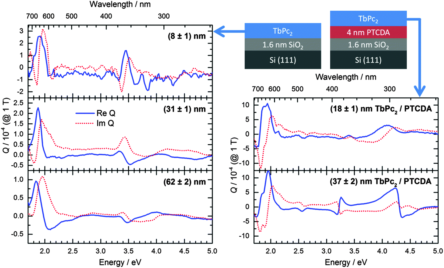
MOKE spectra of TbPc2 recorded for films with thicknesses of (8 ± 1) nm, (31 ± 1) nm, and (62 ± 2) nm are shown in Fig. 1 (left). The red dotted lines represent the imaginary part of the complex Kerr rotation angle, which is related to the ellipticity of the light polarization state after reflection on the magnetized sample. The blue continuous lines represent the real part of the complex Kerr rotation angle, which stems from the rotation of the main axis of the polarization ellipse with respect to the direction of the linear polarization of the incident beam (see sketch in Fig. 1, right).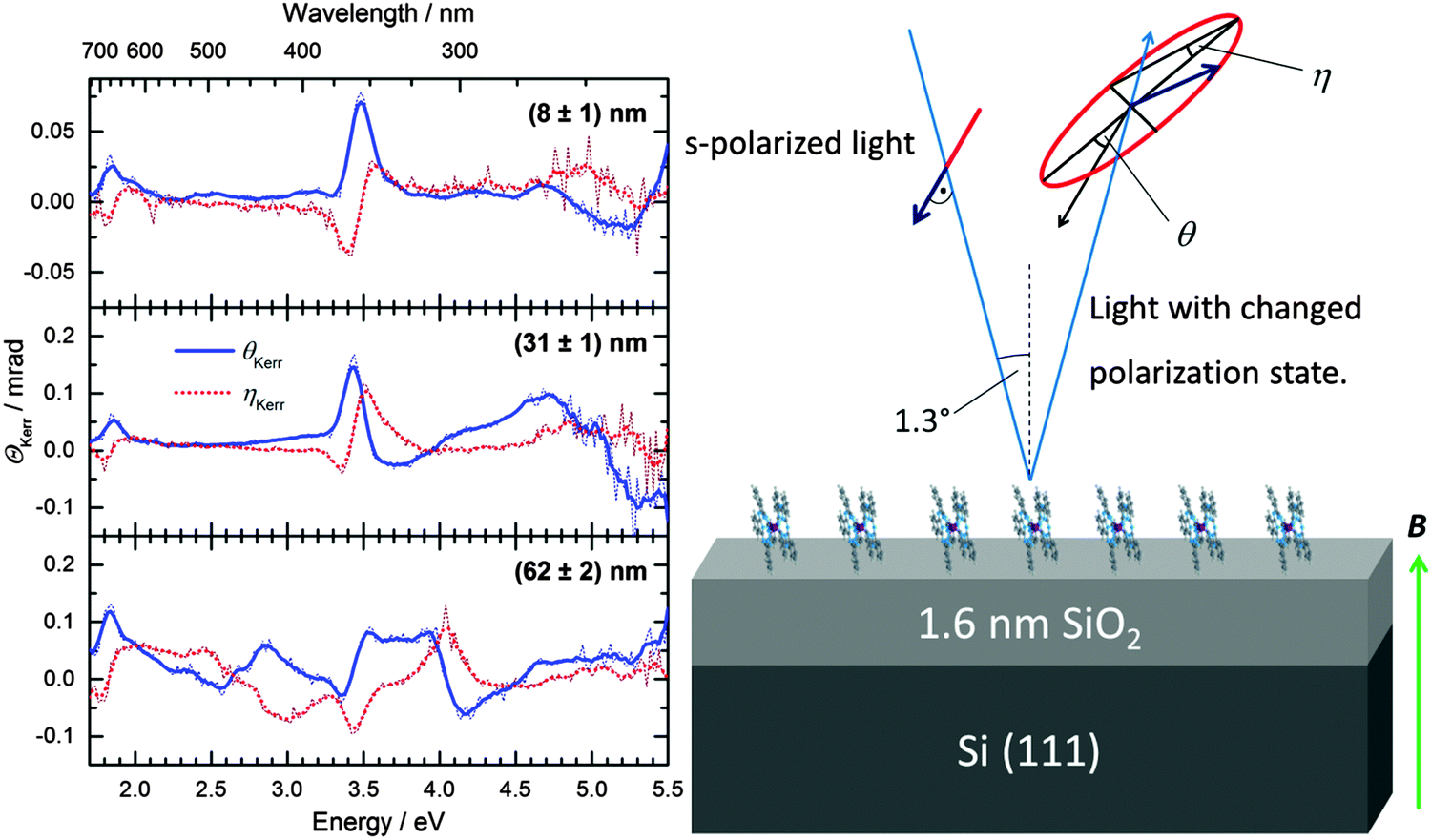 | ||
| Fig. 1 (left) MOKE spectra of TbPc2 films with three different thicknesses grown on SiO2/Si. The continuous lines (blue online) and dotted lines (red online) represent the spectra of the Kerr rotation and the Kerr ellipticity, respectively. The experimental data were averaged over five neighbouring points using the Boxcar filter. (right) Sketch of the measurement geometry. | ||
The prominent peak in the spectra of the thinner films at approximately 3.5 eV stems from the E1 transition of the silicon substrate (see Fig. S3 of the ESI†), since the light penetration depth at this photon energy in TbPc2 is about 80 nm. However, it is remarkable that a magneto-optical activity stemming from the TbPc2 can be detected in the near-infrared and near-ultraviolet for a film as thin as (8 ± 1) nm. With increasing film thickness the features below 2 eV and above 4 eV gain in intensity, which is a clear hint that they originate from optical transitions in TbPc2. In the complex Kerr spectra (Kerr rotation and Kerr ellipticity) of the thickest sample the two features shift and several additional features appear, which overcome in intensity the activity of the Si substrate. In order to interpret the observed spectral changes, the MOKE spectra need to be modelled under consideration of the optical constants and the magneto-optical Voigt constant of TbPc2.
For the determination of the optical constants and the diagonal elements of the dielectric tensor, we employed spectroscopic ellipsometry measurements performed at three angles of incidence (Φ = 50°, 60°, 70°). A first attempt to fit the experimental data using isotropic optical constants was not successful. Subsequently, the experimental data were fitted assuming an uniaxial anisotropy, i.e. the optical constants in the sample plane are different from those perpendicular to it, as it is often the case for single-decker phthalocyanines.22–24 The roughness was taken into account by introducing an additional top layer with optical constants described by the effective media approximation (EMA). Please refer to the ESI† for more details on the fitting model. The resulting optical constants, i.e. the complex refractive indices ñ = n + ik, both in the sample plane (ip) and perpendicular to it (out of plane, oop) are shown in Fig. 2. On the left and right hand side of the figure the refractive index (real part of ñ) and the extinction coefficient k (imaginary part of ñ), respectively, are displayed.
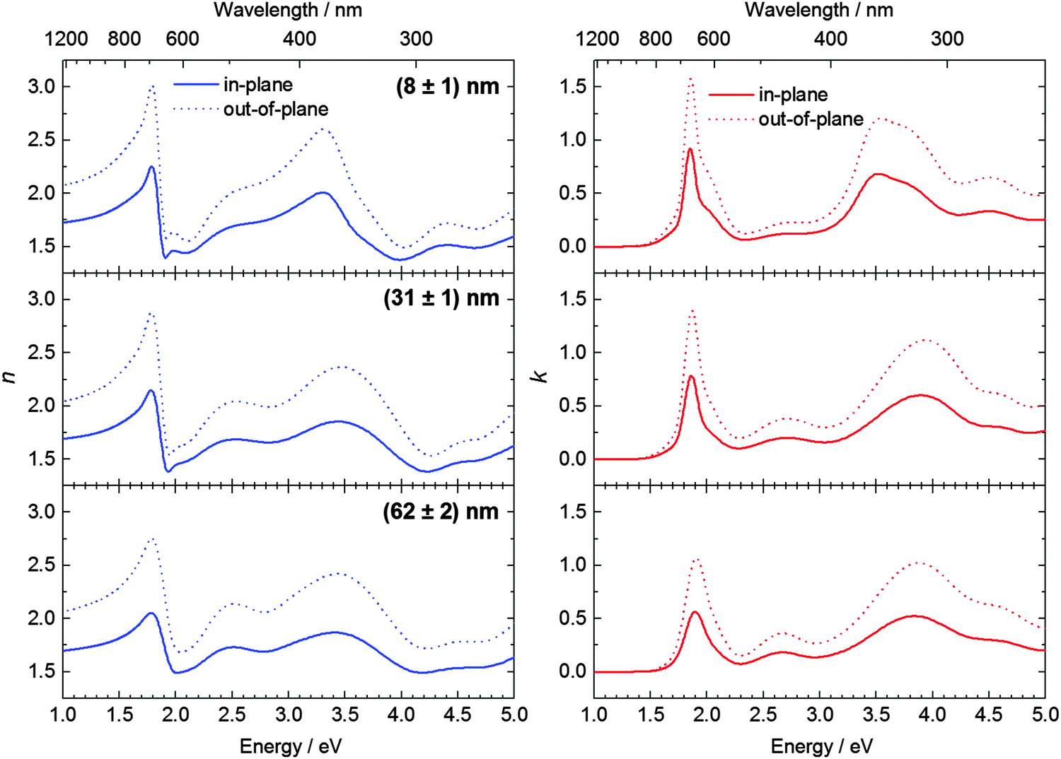 | ||
| Fig. 2 Real part of the refractive index (left) and the extinction coefficient (right) of TbPc2 thin films with different thicknesses. | ||
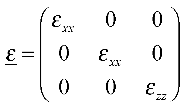
Considering that for organic semiconductors the relative magnetic permeability is μr ≈ 1, we calculate the diagonal components of the dielectric tensor using eqn (1):
| ñii2(ω) = μr·εii(ω) ≈ εii(ω) | (1) |
 | (2) |
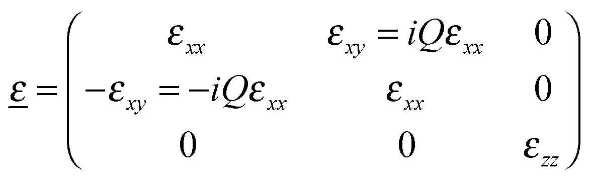
For describing the magneto-optical light–matter interaction the material parameter Q, the so-called Voigt constant (which is photon energy dependent) is the relevant physical quantity. When the magnetic field is perpendicular to the sample surface, along the z axis, two off-diagonal components appear in the dielectric tensor, as shown in eqn (3)22,25
 | (3) |
For experiments performed in transmission geometry, the MCD signal is correlated with the imaginary part of the complex Faraday rotation, ηF, and depends on the Voigt constant as shown in eqn (4):19
 | (4) |
For our MOKE measurements performed in reflection, the dependence of the complex MOKE rotation
| ΘK = θK + iηK | (5) |
 | ||
| Fig. 3 The continuous lines (blue online) and dotted lines (red online) represent the real and the imaginary part of the Voigt constant, respectively, calculated from the in-plane optical constants and from the MOKE spectra for TbPc2 films on SiO2/Si (left) and on PTCDA (right). The values of the Voigt constant are normalized to a magnetic field of 1 T. | ||
Let us now consider the evolution of the optical and magneto-optical constants with the film thickness. The general shape of the extinction spectra shown in Fig. 2 is in very good agreement with UV/vis spectra of TbPc2 dissolved in CH2Cl2.27 The lowest observed energy absorption band, the so-called Q-band, consists of two oscillators at energy positions of (1.86 ± 0.02) eV and (2.00 ± 0.02) eV. They represent ligand-related π → π* optical transitions from the HOMO (highest occupied molecular orbital) to the LUMO+1 and from HOMO−1 to LUMO (lowest unoccupied molecular orbital).28 The magneto-optical activity in the Q-band range is significantly stronger than that in the B-band or Soret-band range (around 3.8 eV), similar to the planar phthalocyanines but in contrast to porphyrins.29 This indicates that the ligand symmetry considerations that govern the selection rules of the (magneto-)optical transitions in planar phthalocyanines remain valid also in the double-decker molecules.29 In contrast to single-decker phthalocyanines, a small absorption band occurs around 2.6 eV, which is above the typical Q-band spectral range and below the typical B-band range of the phthalocyanines.30 It represents electronic transitions from deeper levels to the half-occupied HOMO and it is called the BV-band (blue vibronic).31 The magneto-optical activity of this transition is very weak compared to the other π → π* transitions in the Q- or B-bands and can only be observed in the spectrum of the thickest investigated film (62 nm). Between 3.3 eV and 4.3 eV a broad band is observed in the Q spectra, which corresponds to the B-band of the phthalocyanine ligands. It should be mentioned that the accuracy in determination of its amplitude at the low energy tail is complicated due to the partial overlap in the MOKE (see Fig. S3 of the ESI† and ref. 32) and ellipsometry spectra with the E1 transition in Si. However, the spectral shape of the Voigt constant determined for the thinnest film is in agreement with the MCD results for TbPc2 in solution.27
The peaks of the Voigt constant in the Q-band region are slightly red shifted (about 0.2 eV) in comparison to most single-decker phthalocyanines, e.g. CuPc.19 The value of Q is one order of magnitude higher than for CuPc grown on silicon with native oxide. Nevertheless, the peak positions and the order of magnitude of the Voigt constant for TbPc2 are very similar to VOPc.19 As already shown for H2Pc the Voigt constant can be increased by utilizing a templating layer of perylene-3,4,9,10-tetracarboxylic dianhydride (PTCDA) (Fig. 3).33 This is related to the changed molecular orientation which will be discussed later on.
Remarkably, all features observed in the optical and in the Voigt constant spectra are sharp and intense in the case of the thinnest investigated film ((8 ± 1) nm) and become broader and decrease in magnitude with increasing thickness. The broadening might be related to an increasing strength of excitonic effects. This implies formation and growth of larger crystalline domains. Indeed, AFM topography images shown in Fig. 4 confirm that thicker films consist of larger crystallites. The lower values of the Voigt constant for thicker TbPc2 films on SiO2/Si can be attributed to a small change in molecular orientation, as discussed in the next subsection.
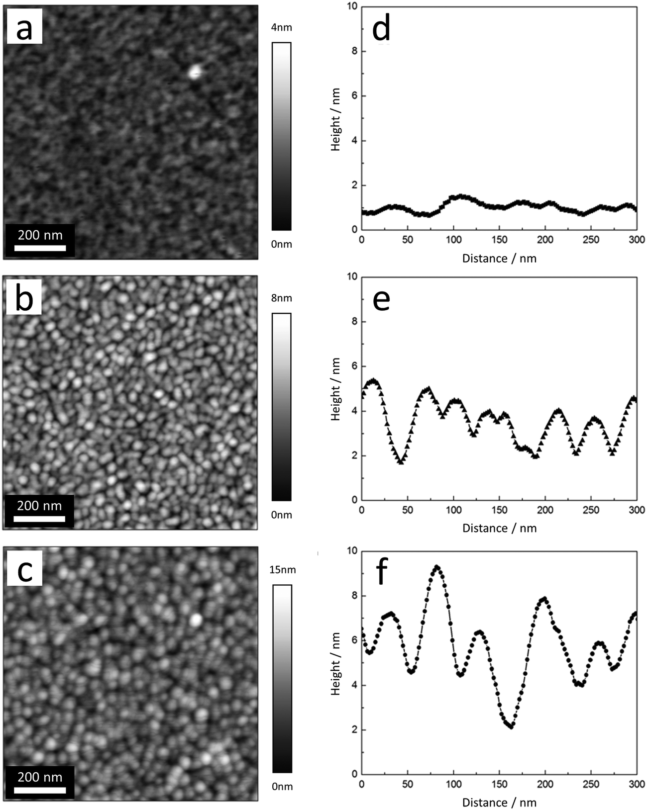 | ||
| Fig. 4 (a–c) AFM topography images and (d–f) typical line profiles of TbPc2 films with average film thicknesses of (a and d) 8 nm, (b and e) 31 nm, and (c and f) 62 nm. | ||
Molecular orientation of TbPc2 on different substrates
The optical anisotropy in molecular layers is caused by the ordering of molecules in crystalline domains. Consequently, the degree of optical anisotropy is influenced by the degree of molecular ordering and by the preferential molecular orientation. This effect was already exploited in order to calculate the average molecular tilt angles with respect to the substrate plane from VASE data for various phthalocyanines, e.g. CuPc23 and H2Pc.33 From the value of the extinction coefficient in the spectral range of the Q-band between 1.5 eV and 2.3 eV the angle between the molecular plane and the substrate plane can be estimated.24 This approach was first used for a double-decker phthalocyanine by Seidel et al.34 The symmetry of the double-decker phthalocyanine molecules is reduced compared to the conventional phthalocyanines. The double-decker phthalocyanines possess only D4d or even D4 symmetry instead of D4h.35 This symmetry lowering is caused by a twisting of the two phthalocyanine skeletons with respect to each other depending on the rare earth metal. However, the selection rules, which are important for the model used for the angle determination, are still valid, namely that the Q- and B-band transitions are polarized in the xy-plane of the ligand, at least in a first approximation.36 Assuming that all molecules adopt the same orientation in thin films, we can apply the formula typically used for planar single-decker phthalocyanines33 to determine the average molecular orientation of the double-deckers on the substrate: | (6) |
| Substrate | Thickness/nm | Tilt angle α/deg |
|---|---|---|
| SiO2/Si | 8 ± 1 | 78 ± 4 |
| 29 ± 1 | 79 ± 4 | |
| 31 ± 1 | 80 ± 4 | |
| 49 ± 2 | 81 ± 4 | |
| 62 ± 2 | 85 ± 4 | |
| PTCDA | 18 ± 1 | 49 ± 6 |
| 37 ± 2 | 61 ± 6 | |
| Co | 18 ± 1 | 67 ± 2 |
| 41 ± 1 | 79 ± 2 | |
| 58 ± 2 | 85 ± 4 | |
| 87 ± 3 | 90 ± 5 | |
This finding of nearly upright molecules holds for various oxide substrates, if we consider the literature reports to date. An overview of the molecular orientation reported on various substrates can be found in Table 2. In all these cases, the first monolayer of the molecules, except for LSMO (La1−xSrxMnO3), was shown or assumed to lie flat on the substrate. These observations are in line with studies on planar phthalocyanine molecules on various metallic substrates, indicating that the interaction between the highest energetic occupied π orbital of the ligand and the substrate governs the molecular orientation of the first layer and the intermolecular interaction determines the orientation in thicker films.37 The results of the few studies on thicker layers (100 nm and above) indicate an upright orientation of the molecules, whenever specified. On oxide substrates such as SiO2, ITO, and LSMO, the molecules tend to adopt a “more upright orientation” already at the interface to the substrate.9,37
| Substrate | TbPc2 film thickness | Molecular orientation | Ref. |
|---|---|---|---|
| Al foil | Few ML | Flat lying upright | L. Margheriti et al., (2010)6 |
| 200 nm | |||
| Au(111) | Isolated molecules | Flat lying | K. Katoh et al., (2009)4 |
| Au (200 nm, polycrystalline) | 100 nm | Upright upright | A. Hofmann et al., (2012)38 |
| 1 μm | |||
| Cu(100) | Isolated molecules | Flat lying | S. Stepanow et al., (2010)5 |
| Cu(111) | Isolated molecules | Flat lying | L. Vitali et al. (2008)3 |
| Co/Ir(111) | Isolated molecules | Flat lying | J. Schwöbel et al., (2012)39 |
| Co (10 ML)/Cu(100) | Isolated molecules | Flat lying | D. Klar et al., (2013)9 |
| Co/Cu(100) | Isolated molecules | Flat lying | L. Malavolti et al., (2013)10 |
| HOPG(0001) (highly oriented pyrolytic graphite) | Isolated molecules | Flat lying | M. Gonidec et al. (2011)40 |
| HOPG | Isolated molecules | Flat lying | D. Klar et al., (2014)41 |
| Ni (13 ML)/Cu(100) & Ni (6 ML)/Ag(100) | 0.05 ± 0.02 ML | Flat lying | A. Lodi Rizzini et al., (2011)8 |
| Ni (15 ML)/Cu(100) | Isolated molecules | Flat lying | D. Klar et al., (2013)9 |
| Mn (3 ML)/Ag(100) | 0.5 ML | Flat lying | A. Lodi Rizzini et al., (2012)7 |
| Graphene | Isolated molecules | Flat lying | A. Candini et al., (2011)11 |
| CoO (3 to 10 ML)/Ag(100) | 0.5 ML | Not specified | A. Lodi Rizzini et al., (2012)8 |
| LSMO | Isolated molecules | Upright | L. Malavolti et al., (2013)10 |
| Quartz | 200 nm | Upright | L. Malavolti et al., (2013)13 |
For the determination of the molecular orientation reported in Table 2 synchrotron based methods, i.e. near edge X-ray absorption fine structure (NEXAFS) and/or X-ray magnetic circular dichroism (XMCD), as well as muon spin relaxation (μSR) were employed.42 For single-decker phthalocyanines, optical lab based methods, such as variable angle spectroscopic ellipsometry, were already applied many times successfully for the determination of the average molecular orientation on various substrates, including opaque substrates, and it was demonstrated that the results are in good agreement with synchrotron based methods like NEXAFS.43,44 STM imaging of single adsorbed molecules as well as of monolayers may also directly confirm the molecular orientation on the substrate for ultrathin films. In this way, e.g. Katoh et al. demonstrated that TbPc2 molecules are lying flat on an Au(111) substrate.12
The magneto-optical response of phthalocyanines depends on the molecular orientation as well. The amplitude of the magneto-optical Kerr signal of single-decker phthalocyanines scales, in a first approximation, with the cosine of the molecular tilt angle.33 A tilt angle of 0° corresponds here to flat lying molecules on a surface. We, therefore, expect that if the TbPc2 molecules would lie flat on the substrate, the MOKE signal can be increased.
According to previous literature reports (see Table 2), one possibility to grow thin films of TbPc2 with the molecules lying parallel to the substrate plane would be to use metallic single crystal substrates. We fabricated TbPc2 films with various thicknesses on 25 nm thick polycrystalline Co films deposited on Si covered with SiO2, in order to mimic a heterostructure that can be found in a spin valve. The TbPc2 morphology and roughness is similar to that of the films grown on SiO2/Si, cf.ref. 14. The average tilt angle determined from ellipsometry measurements for TbPc2 in an 18 nm thin film is ca. 11° lower than the angle obtained for a similar sample on SiO2/Si. However, the average tilt angle (ca. 67°) for such a film thickness is still far from flat lying molecules. This can be attributed to the finite roughness of the Co films.
Another possibility to obtain lying molecules is to exploit the template effect of a thin layer of aromatic molecules that are known to adopt parallel orientation on various substrates. This method was proven to be successful for the case of H2Pc grown on PTCDA/SiO2/Si (see e.g.ref. 33). The morphology and roughness of the TbPc2 films deposited onto the PTCDA layer are similar to those grown on SiO2/Si. Fig. 5 shows the topography of the PTCDA and the Co films as well as the heterostructures.
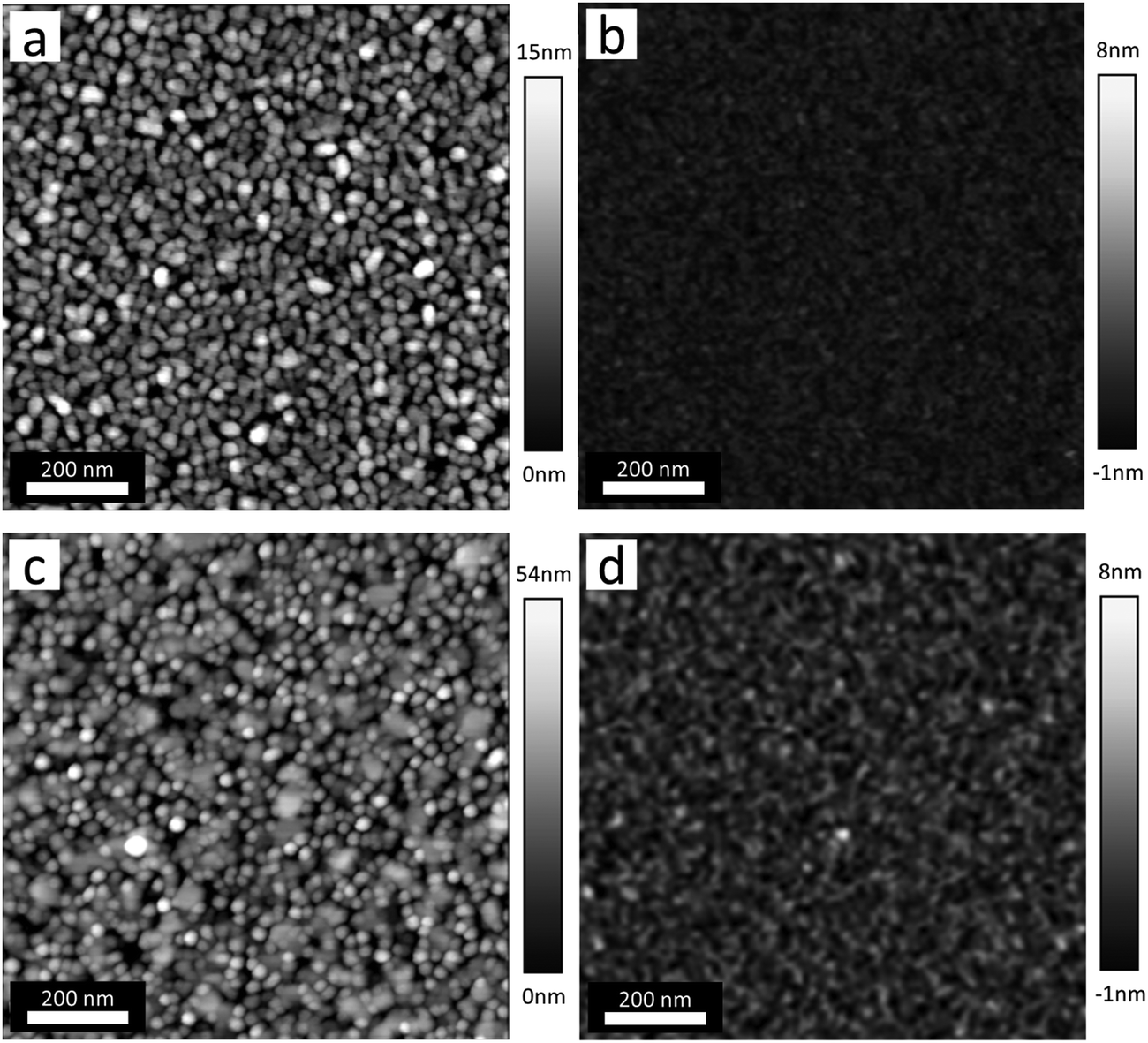 | ||
| Fig. 5 AFM topography images. (a) 4 nm PTCDA on SiO2/Si. (b) 25 nm Co on SiO2/Si. (c) 18 nm TbPc2 on PTCDA. (d) 18 nm TbPc2 on Co. | ||
The optical constants of TbPc2/PTCDA determined from the ellipsometry data can be found in Fig. S7 of the ESI.† The dielectric function of a (58 ± 2) nm thick film of TbPc2 on Co was published elsewhere.14 From the dielectric function, the complex refractive index for all investigated TbPc2 films on Co was calculated and included in Fig. S8 of the ESI† as a function of the film thickness starting with (18 ± 1) nm. The general lineshape of the optical constants does not change significantly with the film thickness and is similar to that of TbPc2/SiO2 or TbPc2/PTCDA. According to our ellipsometry results, the presence of a 4 nm PTCDA layer at the interface between TbPc2 and SiO2/Si has a stronger effect on the molecular orientation of TbPc2 as compared to the 25 nm thick polycrystalline Co film (cf.Table 1). For example, in the case of the 8 nm TbPc2 film on SiO2/Si, the angle α amounts to (78 ± 4)°, while for 18 nm TbPc2 films on PTCDA and Co, the angle α amounts to (49 ± 6)° and (67 ± 2)°, respectively. Please note that with increasing film thickness the templating effect on the molecular orientation decreases and finally vanishes.
Magnetic characterization
For verifying the molecular orientation revealed by optical studies SQUID-VSM investigations of a (43 ± 1) nm thick TbPc2 film on SiO2/Si and of a (37 ± 2) nm thick TbPc2 film on 4 nm PTCDA/Kapton as well as of a (2.6 ± 0.1) mg TbPc2 powder sample were performed at nine different temperatures with the magnetic field applied parallel to the sample surface (see Fig. 6). For TbPc2/Co/SiO2/Si it was not possible to extract the magnetic properties of the TbPc2 film due to the significantly higher signal from the ferromagnetic Co layer. The SMM properties of both TbPc2 films and powder can be described by a spin Hamiltonian as illustrated in the ESI.†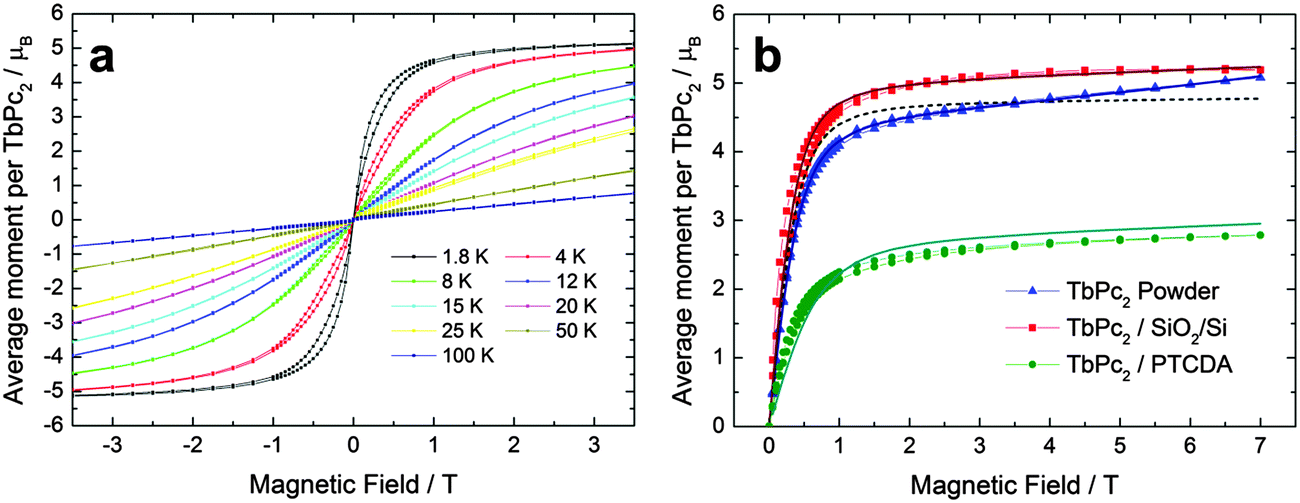 | ||
| Fig. 6 (a) Magnetic hysteresis loops of a 43 nm TbPc2 thin film on SiO2/Si at different temperatures measured by SQUID magnetometry. (b) Comparison between the hysteresis loops of the TbPc2 film on SiO2/Si (red squares), on PTCDA/Kapton (green circles), and powder (blue triangles) at a temperature of 1.8 K. The solid lines represent the fitting using a spin Hamiltonian. The dashed line shows the simulation using the ligand field parameters of Ishikawa et al.46 Simulations and fitting were performed using the PHI software.47 | ||
The hysteresis loops exhibit the typical butterfly shape up to 8 K in the case of the films (Fig. 6a). A comparison between the hysteresis loops of the film and of the powder at 1.8 K (Fig. 6b) shows that the thin film saturates much faster than the powder sample. This can be related to a good degree of ordering of the SMMs in the films, compared to the polycrystalline powder sample. As the magnetic field is applied parallel to the film surface in this experiment, and considering that the easy axis of magnetization of TbPc2 is perpendicular to the ligand planes, the fast saturation of the film hysteresis is consistent with the model of standing molecules in the film on SiO2/Si and closer to lying in the film on PTCDA (resulting from ellipsometry data analysis). The opening of the butterfly shaped hysteresis is larger in the films compared to the powder, probably due to a more pronounced tunneling probability in the powder. Such an effect was already observed on different substrates.13,45
Enhancing the magneto-optical response of TbPc2
The molecular orientation of TbPc2 has a significant effect on the magnitude of the MOKE signal. The Kerr rotation in the films grown on PTCDA (Fig. 7, left) is increased by up to one order of magnitude compared to the films on bare silicon substrates. Thanks to the signal enhancement the two Q-band transitions become distinguishable, which was not the case for the samples without any templating. It has to be mentioned that the peak at 2.6 eV can stem from the BV-band of the TbPc2 or the Q-band absorption of the PTCDA. However, the presence of a peak at the very same energy in the spectrum of the 58 nm thick sample on Co (Fig. 7, right) suggests that it originates from the TbPc2 layer. The MOKE signal enhancement can be simulated considering an increase in the Voigt constant of TbPc2 (Fig. 3, right hand side), which is consistent with a decreasing molecular tilt angle.19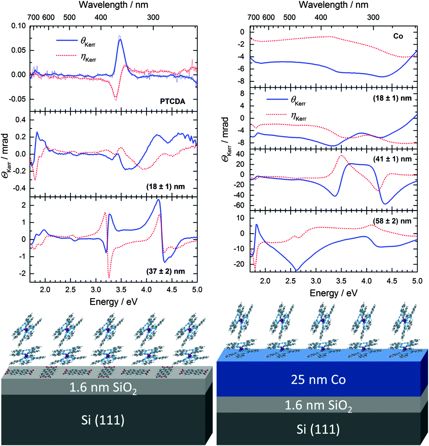 | ||
| Fig. 7 (left) MOKE spectra of TbPc2 films with two different thicknesses grown on PTCDA/SiO2/Si. The upper graph shows the spectrum of PTCDA/SiO2/Si. (right) MOKE spectra of TbPc2 films on Co/SiO2/Si. The continuous lines (blue online) and dotted lines (red online) represent the spectra of the Kerr rotation and the Kerr ellipticity, respectively. The experimental data were averaged over five neighbouring points using the Boxcar filter. (bottom) Sketch of the investigated samples. | ||
The blank Co substrate exhibits a signal of several mrad. As already observed for organic/ferromagnetic heterostructures, the thickness of the organic (dielectric) layer can modulate the magneto-optical activity of the ferromagnetic layer (see e.g.ref. 26 and references therein). The broad features of cobalt are then accompanied by sharp peaks related to the TbPc2 transitions. For the TbPc2 features an enhancement of the Kerr rotation by up to two orders of magnitude can be achieved compared to the films on SiO2/Si substrates, though the difference in molecular orientation is less than for the films on PTCDA substrates. This enhancement leads to signals of up to 60 mrad (3.4°) that are easily detectable with typical magneto-optical reading heads of data storage devices.48
Summary
In this work we fabricated thin films (from 8 nm to 87 nm) of the SMM TbPc2 by thermal evaporation in vacuum on several substrates, which can be regarded as model systems for organic electronic and spintronic applications. The effects of the substrate and of the increasing film thickness on the film morphology, molecular orientation, as well as on the optical and magneto-optical properties were investigated.By combining spectroscopic ellipsometry and MOKE results, we determined for the first time the optical and magneto-optical constants of thin films of TbPc2. The magneto-optical Voigt constant of the films shows that the magneto-optical activity of TbPc2 is about one order of magnitude larger than that of planar transition metal phthalocyanines. By introducing an organic templating layer of PTCDA it was possible to enhance the magneto-optical response of TbPc2 layers by up to one order of magnitude, while by using a cobalt substrate an increase of the Kerr rotation of up to two orders of magnitude was achieved.
Our observations open new perspectives for combining magnetism and optics in devices such as spin-OFETs and spin valves. The change in the polarization state of a linearly polarized light beam reflected by an active layer of TbPc2 might be used as a diagnosis tool for eventual electronic changes under applied electric/magnetic field in the spintronic device. On the other hand, by illuminating the TbPc2 film in such devices with circularly polarized light of suitable photon energy, the control on the spin polarization of the electrical current might be strived for, similar to reports in inorganic spintronic devices.49
Acknowledgements
We gratefully acknowledge the financial support from the Deutsche Forschungsgemeinschaft (DFG) in the frame of the Research Unit FOR 1154 “Towards Molecular Spintronics”.Notes and references
- N. Ishikawa, M. Sugita, T. Ishikawa, S. Koshihara and Y. Kaizu, J. Am. Chem. Soc., 2003, 125, 8694–8695 CrossRef CAS PubMed.
- A. Lodi Rizzini, C. Krull, A. Mugarza, T. Balashov, C. Nistor, R. Piquerel, S. Klyatskaya, M. Ruben, P. M. Sheverdyaeva, P. Moras, C. Carbone, C. Stamm, P. S. Miedema, P. K. Thakur, V. Sessi, M. Soares, F. Yakhou-Harris, J. C. Cezar, S. Stepanow and P. Gambardella, Surf. Sci., 2014, 630, 361–374 CrossRef CAS PubMed.
- L. Vitali, S. Fabris, A. M. Conte, S. Brink, M. Ruben, S. Baroni and K. Kern, Nano Lett., 2008, 8, 3364–3368 CrossRef CAS PubMed.
- K. Katoh, Y. Yoshia, M. Yamashita, H. Miyasaka, B. K. Breedlove, T. Kajiwara, S. Takaishi, N. Ishikawa, H. Isshiki, Y. F. Zhang, T. Komeda, M. Yamagishi and J. Takeya, J. Am. Chem. Soc., 2009, 131, 9967–9976 CrossRef CAS PubMed.
- S. Stepanow, J. Honolka, P. Gambardella, L. Vitali, N. Abdurakhmanova, T. Tseng, S. Rauschenbach, S. L. Tait, V. Sessi, S. Klyatskaya, M. Ruben and K. Kern, J. Am. Chem. Soc., 2010, 132, 11900–11901 CrossRef CAS PubMed.
- L. Margheriti, D. Chiappe, M. Mannini, P. Car, P. Sainctavit, M. Arrio, F. B. de Mongeot, J. C. Cezar, F. M. Piras, A. Magnani, E. Otero, A. Caneschi and R. Sessoli, Adv. Mater., 2010, 22, 5488–5493 CrossRef CAS PubMed.
- A. Lodi Rizzini, C. Krull, T. Balashov, A. Mugarza, C. Nistor, F. Yakhou, V. Sessi, S. Klyatskaya, M. Ruben, S. Stepanow and P. Gambardella, Nano Lett., 2012, 12, 5703–5707 CrossRef CAS PubMed.
- A. Lodi Rizzini, C. Krull, T. Balashov, J. J. Kavich, A. Mugarza, P. S. Miedema, P. K. Thakur, V. Sessi, S. Klyatskaya, M. Ruben, S. Stepanow and P. Gambardella, Phys. Rev. Lett., 2011, 107, 177205 CrossRef CAS.
- D. Klar, S. Klyatskaya, A. Candini, B. Krumme, K. Kummer, P. Ohresser, V. Corradini, V. de Renzi, R. Biagi, L. Joly, J.-P. Kappler, U. del Penninho, M. Affronte, H. Wende and M. Ruben, Beilstein J. Nanotechnol., 2013, 4, 320–324 CrossRef PubMed.
- L. Malavolti, L. Poggini, L. Margheriti, D. Chiappe, P. Graziosi, B. Cortigiani, V. Lanzilotto, F. Buatier de Mongeot, P. Ohresser, E. Otero, F. Choueikani, P. Sainctavit, I. Bergenti, V. A. Dediu, M. Mannini and R. Sessoli, Chem. Commun., 2013, 49, 11506–11508 RSC.
- A. Candini, S. Klyatskaya, M. Ruben, W. Wernsdorfer and M. Affronte, Nano Lett., 2011, 11, 2634–2639 CrossRef CAS PubMed.
- K. Katoh, T. Komeda and M. Yamashita, Dalton Trans., 2010, 39, 4708–4723 RSC.
- L. Malavolti, M. Mannini, P. E. Car, G. Campo, F. Pineider and R. Sessoli, J. Mater. Chem. C, 2013, 1, 2935–2942 RSC.
- P. Robaschik, P. F. Siles, D. Bülz, P. Richter, M. Monecke, M. Fronk, S. Klyatskaya, D. Grimm, O. G. Schmidt, M. Ruben, D. R. T. Zahn and G. Salvan, Beilstein J. Nanotechnol., 2014, 5, 2070–2078 CrossRef CAS PubMed.
- R. Vincent, S. Klyatskaya, M. Ruben, W. Wernsdorfer and F. Balestro, Nature, 2012, 488, 357–360 CrossRef CAS PubMed.
- S. Thiele, F. Balestro, R. Ballou, S. Klyatskaya, M. Ruben and W. Wernsdorfer, Science, 2014, 344, 1135–1138 CrossRef CAS PubMed.
- F. Branzoli, P. Carretta, M. Filibian, M. J. Graf, S. Klyatskaya, M. Ruben, F. Coneri and P. Dhakal, Phys. Rev. B: Condens. Matter Mater. Phys., 2010, 82, 134401 CrossRef.
- Spectroscopic Ellipsometry Software WVASE32 – J. A. Woollam Co., http://www.jawoollam.com/wvase.html.
- M. Fronk, B. Bräuer, J. Kortus, O. G. Schmidt, D. R. T. Zahn and G. Salvan, Phys. Rev. B: Condens. Matter Mater. Phys., 2009, 79, 235305 CrossRef.
- Gwyddion – Free SPM (AFM, SNOM/NSOM, STM, MFM,…) data analysis software, http://gwyddion.net/.
- S. Heutz, C. Mitra, W. Wu, A. J. Fisher, A. Kerridge, M. Stoneham, T. H. Harker, J. Gardener, H.-H. Tseng, T. S. Jones, C. Renner and G. Aeppli, Adv. Mater., 2007, 19, 3618–3622 CrossRef CAS PubMed.
- J. Zak, E. R. Moog, C. Liu and S. D. Bader, Phys. Rev. B: Condens. Matter Mater. Phys., 1991, 43, 6423 CrossRef.
- O. D. Gordan, M. Friedrich and D. R. T. Zahn, Org. Electron., 2004, 5, 291–297 CrossRef CAS PubMed.
- O. D. Gordan, M. Friedrich and D. R. T. Zahn, Thin Solid Films, 2004, 455, 551–556 CrossRef PubMed.
- A. Bauer, Habilitation thesis, FU, Berlin, 2000 Search PubMed.
- W. Li, M. Fronk, H. Kupfer, S. Schulze, M. Hietschold, D. R. T. Zahn and G. Salvan, J. Am. Chem. Soc., 2010, 132, 5687–5692 CrossRef CAS PubMed.
- M. Gonidec, E. S. Davies, J. McMaster, D. B. Amabilino and J. Veciana, J. Am. Chem. Soc., 2010, 132, 1756–1757 CrossRef CAS PubMed.
- K. Yoshino, S. B. Lee, T. Sonoda, H. Kawagishi, R. Hidayat, K. Nakayama, M. Ozaki, K. Ban, K. Nishizawa, K. Ohta and H. Shirai, J. Appl. Phys., 2000, 88, 7137–7143 CrossRef CAS PubMed.
- T. Birnbaum, T. Hahn, C. Martin, J. Kortus, M. Fronk, F. Lungwitz, D. R. T. Zahn and G. Salvan, J. Phys.: Condens. Matter, 2014, 26, 104201 CrossRef PubMed.
- A. T. Davidson, J. Chem. Phys., 1982, 77, 168–172 CrossRef CAS PubMed.
- E. Orti, J. L. Brédas and C. Clarisse, J. Chem. Phys., 1990, 92, 1228–1235 CrossRef CAS PubMed.
- M. Fronk, S. Müller, T. Waechtler, S. E. Schulz, R. Mothes, H. Lang, D. R. T. Zahn and G. Salvan, Thin Solid Films, 2012, 520, 4741–4744 CrossRef CAS PubMed.
- B. Bräuer, M. Fronk, D. Lehmann, D. R. T. Zahn and G. Salvan, J. Phys. Chem. B, 2009, 113, 14957 CrossRef PubMed.
- F. Seidel, M. Fronk, C. Himcinschi, V. Chis and D. R. T. Zahn, Phys. Status Solidi C, 2010, 2, 222–226 CrossRef PubMed.
- Y. Fu, J. Schwöbel, S. Hla, A. Dilullo, G. Hoffmann, S. Klyatskaya, M. Ruben and R. Wiesendanger, Nano Lett., 2012, 12, 3931–3935 CrossRef CAS PubMed.
- T. C. Vancott, Z. Gasyna, P. N. Schatz and M. E. Boyle, J. Phys. Chem., 1995, 99, 4820–4830 CrossRef CAS.
- I. Biswas, H. Peisert, M. B. Casu, B. E. Schuster, P. Nagel, M. Merz, S. Schuppler and T. Chasse, Phys. Status Solidi A, 2009, 206, 2524–2528 CrossRef CAS PubMed.
- A. Hofmann, Z. Salman, M. Mannini, A. Amato, L. Malavolti, E. Morenzoni, T. Prokscha and R. Sessoli, ACS Nano, 2012, 6, 8390–8396 CrossRef CAS PubMed.
- J. Schwöbel, Y. Fu, J. Brede, A. Dilullo, G. Hoffmann, S. Klyatskaya, M. Ruben and R. Wiesendanger, Nat. Commun., 2012, 3, 953 CrossRef PubMed.
- M. Gonidec, R. Biagi, V. Corradini, F. Moro, V. De Renzi, U. del Pennino, D. Summa, L. Muccioli, C. Zannoni, D. B. Amabilino and J. Veciana, J. Am. Chem. Soc., 2011, 133, 6603–6612 CrossRef CAS PubMed.
- D. Klar, A. Candini, J. Loïc, S. Klyatskaya, B. Krumme, P. Ohresser, J.-P. Kappler, M. Ruben and H. Wende, Dalton Trans., 2014, 43, 10686–10689 RSC.
- F. Branzoli, M. Filibian, P. Carretta, S. Klyatskaya and M. Ruben, Phys. Rev. B: Condens. Matter Mater. Phys., 2009, 79, 220404 CrossRef.
- M. Friedrich, G. Gavrila, C. Himcinschi, T. U. Kampen, A. Yu Kobitski, H. Méndez, G. Salvan, I. Cerilló, J. Méndez, N. Nicoara, A. M. Baró and D. R. T. Zahn, J. Phys.: Condens. Matter, 2003, 15, 2699–2718 CrossRef.
- T. U. Kampen, G. Salvan, A. Paraian, C. Himcinschi, A. Yu Kobitski, M. Friedrich and D. R. T. Zahn, Appl. Surf. Sci., 2003, 212, 501–507 CrossRef.
- M. Mannini, F. Bertani, C. Tudisco, L. Malavolti, L. Poggini, K. Misztal, D. Menozzi, A. Motto, E. Otero, P. Ohresser, P. Sainctavit, G. G. Condorelli, E. Dalcanale and R. Sessoli, Nat. Commun., 2014, 5, 4582 CAS.
- N. Ishikawa, M. Sugita, T. Okubo, N. Tanaka, T. Iino and Y. Kaizu, Inorg. Chem., 2003, 42, 2440–2446 CrossRef CAS PubMed.
- N. F. Chilton, R. P. Anderson, L. D. Turner, A. Soncini and K. S. Murray, J. Comput. Chem., 2013, 34, 1164–1175 CrossRef CAS PubMed.
- W. M. Steen, Laser Material Processing, Springer-Verlag London, London, UK, 2003 Search PubMed.
- S. A. Wolf, D. D. Awschalom, R. A. Burman, J. M. Daughton, S. von Molnár, M. L. Roukes, A. Y. Chtchelkanova and D. M. Treger, Science, 2001, 294, 1488–1495 CrossRef CAS PubMed.
Footnotes |
| † Electronic supplementary information (ESI) available: Maldi-ToF spectrum of [TbPc2]0 (Fig. S1). UV/vis/nIR spectrum of [TbPc2]0 (Fig. S2). MOKE spectrum of a blank Si substrate (Fig. S3). VASE spectra of one sample and the model fit (Fig. S4), and in-plane components (Fig. S5), as well as the out-of-plane components of the dielectric tensor (Fig. S6) of the TbPc2 films grown on SiO2/Si. Complex refractive index of TbPc2/PTCDA (Fig. S7). Complex refractive index of TbPc2/Co (Fig. S8). Ligand field parameters of TbPc2 powder and film (Table S1). See DOI: 10.1039/c5tc01520k |
| ‡ Present address: Department of Materials and London Centre for Nanotechnology, Imperial College London, London SW7 2AZ, UK. |
| This journal is © The Royal Society of Chemistry 2015 |