
Ferroelectricity in Dion–Jacobson ABiNb2O7 (A = Rb, Cs) compounds†
Chen
Chen
a,
Huanpo
Ning
a,
Serban
Lepadatu
b,
Markys
Cain
b,
Haixue
Yan
a and
Mike J.
Reece
*a
aSchool of Engineering and Materials Science, Queen Mary University of London, London E1 4NS, UK. E-mail: m.j.reece@qmul.ac.uk
bNational Physical Laboratory, Teddington, Middlesex TW11 0LW, UK
First published on 4th November 2014
Abstract
The ferroelectric properties of 2-layer Dion–Jacobson compounds ABiNb2O7 (A = Rb and Cs) were studied. Ferroelectricity and piezoelectricity of CsBiNb2O7 were demonstrated for the first time. The ferroelectric domain structure of Dion–Jacobson compounds were imaged using PFM. The Curie points of RbBiNb2O7 and CsBiNb2O7 are 1098 ± 5 and 1033 ± 5 °C, respectively. The piezoelectric constant of RbBiNb2O7 and CsBiNb2O7 are approximately 5 and 8 pC N−1. Thermal depoling was also studied to confirm the Curie temperature and the stability of the piezoelectricity.
Perovskite-like layered structured (PLS) compounds display a range of interesting physical and chemical properties, including photocatalysis, photoluminescence, ion conductivity, electrochemical stability, magnetic properties, ferroelectricity and piezoelectricity.1–7 Generally, the perovskite layers of PLS materials are formed by corner-sharing BO6 octahedra separated by oxygen rich layers. There are mainly three homologous series of PLS materials according to their different BO6 octahedra orientation: the Dion–Jacobson type phases (A′An−1BnO3n+1); the AnBnO3n+2 type phases; and the hexagonal phases (AnBn−1O3n).1 The crystal structure of Dion–Jacobson phase can be regarded as a result of cutting the idealized perovskite structure across the (1 0 0)perovskite plane, and the crystal structure of AnBnO3n+2 phase and the hexagonal phase can be regarded as a result of cutting the perovskite structure across the (1 1 0)perovskite and (1 1 1)perovskite planes, respectively.1,8 The AnBnO3n+2 type PLS materials have been shown to be ferroelectrics with super high Curie point, especially the 4-layer La2Ti2O7 and Sr2Nb2O7 phases, which have Curie point above 1300 °C.9–11 However, materials with Dion–Jacobson structure and Hexagonal structure have rarely been reported to present ferroelectricity.
The crystal structure of the Dion–Jacobson compound CsBiNb2O7 was studied by Snedden, et al. and found to have similar structural distortions to that of ferroelectric Aurivillius phase SrBi2Ta2O9, but they concluded that CsBiNb2O7 does not display ferroelectricity according to dielectric measurements.12,13 Recently, Fennie et al. demonstrated the polar nature of CsBiNb2O7 using first principles and group theoretical analysis and estimated that CsBiNb2O7 has a spontaneous polarization of 40 μC cm−2.14 More recently, Goff et al. reported that the ferroelectricity of CsBiNb2O7 cannot be detected due to its large leakage current and significant proton conductivity.15 Recently, the ferroelectricity and piezoelectricity of RbBiNb2O7, which has similar crystal structure to CsBiNb2O7, was reported by Li et al.,16 which made us to reconsider the possibility of discovering ferroelectricity for CsBiNb2O7.
In this work, we present the ferroelectricity and piezoelectricity of ABiNb2O7 (A = Rb, Cs) ceramics by direct evidence of ferroelectric domain switching and piezoelectric activity. The ferroelectric domain structures of CsBiNb2O7 and RbBiNb2O7 were investigated using PFM images. The Curie point for CsBiNb2O7 and RbBiNb2O7 were found to be 1033 ± 5 and 1098 ± 5 °C by studying the temperature dependence of permittivity and thermal depoling.
Fig. 1 shows the XRD patterns of ABiNb2O7 powders measured at room temperature. Both the powders of CsBiNb2O7 and RbBiNb2O7 are single phase, and no impurity can be observed in the XRD patterns. CsBiNb2O7 and RbBiNb2O7 have the same 2-layer Dion–Jacobson structure at room temperature, which is orthorhombic and belongs to space group P21am (26).13,14,16 The lattice parameters are a = 5.4964, b = 5.4223 and c = 11.3704 Å for CsBiNb2O7 and a = 5.4193, b = 5.3589 and c = 11.2099 Å for RbBiNb2O7. Their spontaneous polarization directions are along the a-axis. The insets in Fig. 1 show the SEM images of the plate-like powders. Due to the plate-like grain shape, preferred orientation of the (0 0 l) plane can be observed in the powders. After SPS sintering, greater preferred (0 0 l) orientation was found in the ceramics (Fig. S1†). The orientation factors for CsBiNb2O7 and RbBiNb2O7 ceramic were 0.9 and 0.7, respectively. The benefit of orientation is to decrease the coercive field for polarization switching.
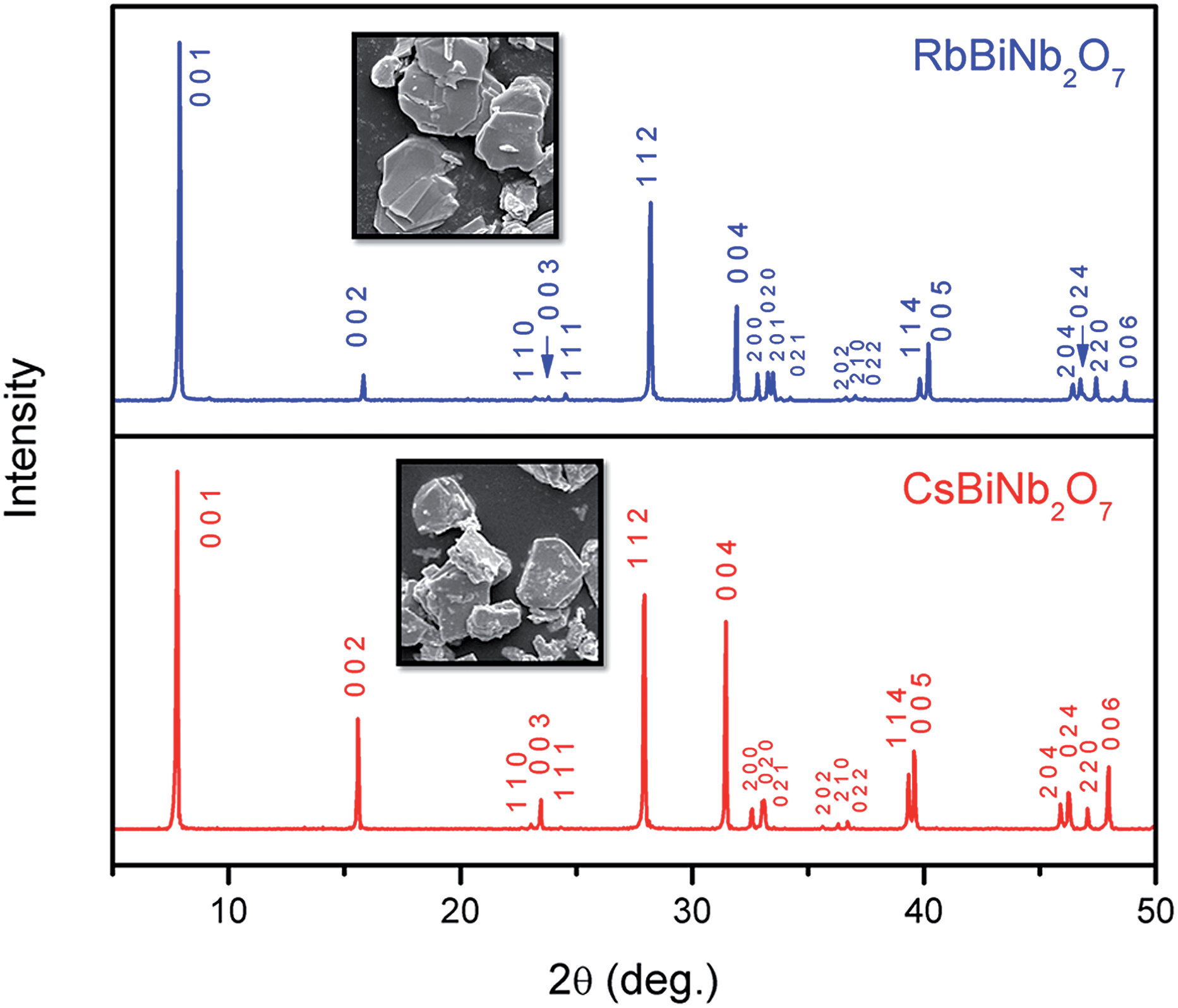 | ||
| Fig. 1 X-ray diffraction patterns of ABiNb2O7 powders. | ||
Fig. 2 shows the HRTEM images of ABiNb2O7 ceramics. Unfaulted lattice planes were observed for both CsBiNb2O7 (Fig. 2(a)) and RbBiNb2O7 (Fig. 2(b)). The d-pacing of the lattice planes was measured to be 1.12 ± 0.02 nm for CsBiNb2O7 and 1.08 ± 0.02 nm for RbBiNb2O7. Selected area electron diffraction patterns are shown in insets in Fig. 2(a) and (b). The linear reflections were indexed to be (0 0 l) lattice planes. The d-spacing of the (0 0 l) plane, which corresponds to the length of c axis of the unit cell, was measured to be 1.13 ± 0.02 nm for CsBiNb2O7 and 1.10 ± 0.02 nm for RbBiNb2O7.
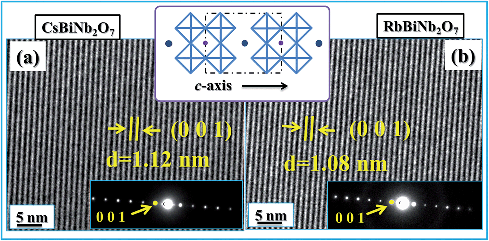 | ||
| Fig. 2 HRTEM images of ABiNb2O7 ceramics: (a) CsBiNb2O7; (b) RbBiNb2O7. | ||
Fig. 3 shows vertical-mode PFM images of CsBiNb2O7 ceramic. Because the SPS sintered ceramics were highly textured on the (0 0 l) plane and the polar axis is in the a-direction, samples with surfaces perpendicular to SPS pressing direction were prepared to investigate the ferroelectric domain structure with PFM. Several grains with clear grain boundaries can be observed in the topography image shown in Fig. 3(a). Ferroelectric domain morphology is clearly observed in the PFM amplitude and phase images (Fig. 3(b) and (c)). Bright areas in the amplitude image reveal the stripe domains with vertical piezo-response signal. Some of the dark areas reveal regions with in-plane polarization. The bright and dark areas in the phase image reveal the up and down out-of-plane polarization, respectively. Comparing the PFM amplitude and phase images with the topography image, clear ferroelectric domains can be observed in several grains (A to E), and stripe domains with different orientations show strong contrast in each grain. Fig. 3(d) shows the schematic of the out-of-plane and in-plane polarization in grain A. The black, yellow and orange stripes represent the dark, bright and grey areas. The polarization direction can be indexed through comparing the phase and amplitude images. The width of the domains was typically from 10 to 600 nm. Similar ferroelectric domain structure was also observed for RbBiNb2O7 ceramic (Fig. S2†).
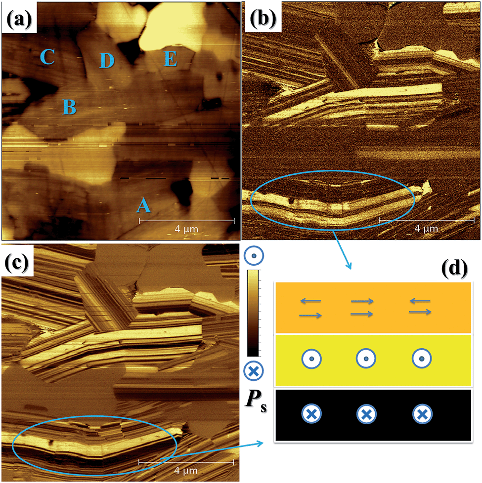 | ||
| Fig. 3 Vertical-mode PFM images of CsBiNb2O7 ceramic: (a) topography; (b) amplitude; (c) phase and (d) schematic of the selected area from (c). | ||
The temperature dependence of dielectric constants of CsBiNb2O7 and RbBiNb2O7 are shown in Fig. 4(a). The Curie point, Tc, of CsBiNb2O7 and RbBiNb2O7 are 1033 ± 5 and 1098 ± 5 °C, respectively. The ferroelectric-to-paraelectric phase transition temperature for CsBiNb2O7 is demonstrated for the first time. Goff et al. reported that the orthorhombic phase of CsBiNb2O7 was stable from room temperature to 900 °C and no ferroelectric orthorhombic to paraelectric tetragonal phase transition was observed using high-temperature XRD,15 which is in agreement with our result that the Tc of CsBiNb2O7 is above 900 °C (∼1033 °C). The Tc of RbBiNb2O7 was first reported to be 943 °C by Li et al.,16 which is about 155 °C lower than our result. To calibrate our equipment, the Tc of LiNbO3 single crystal was measured with the same equipment. The Tc of LiNbO3 was measured as ∼1138 °C. According to the literature,17 the Tc of single crystal LiNbO3 is 1140 °C, which means that the Tc values we measured are relatively accurate. The insets of Fig. 4(a) show the current–electric field (I–E) and electric displacement–electric field (D–E) hysteresis loops of CsBiNb2O7 and RbBiNb2O7. The I–E and D–E loops were measured at 110 °C and 10 Hz for CsBiNb2O7. A typical, unsaturated, ferroelectric D–E loop obtained for CsBiNb2O7 is shown in the inset of Fig. 4(a). In its I–E loop, a current peak (marked by arrow) produced by ferroelectric domain switching is observed. For RbBiNb2O7, I–E and D–E loops, measured at 200 °C and 100 Hz, are shown in the inset of Fig. 4(a). A typical vesica piscis-shaped D–E loop due to leakage current was observed, but the ferroelectric domain switching is demonstrated by the peak observed in the I–E loop.
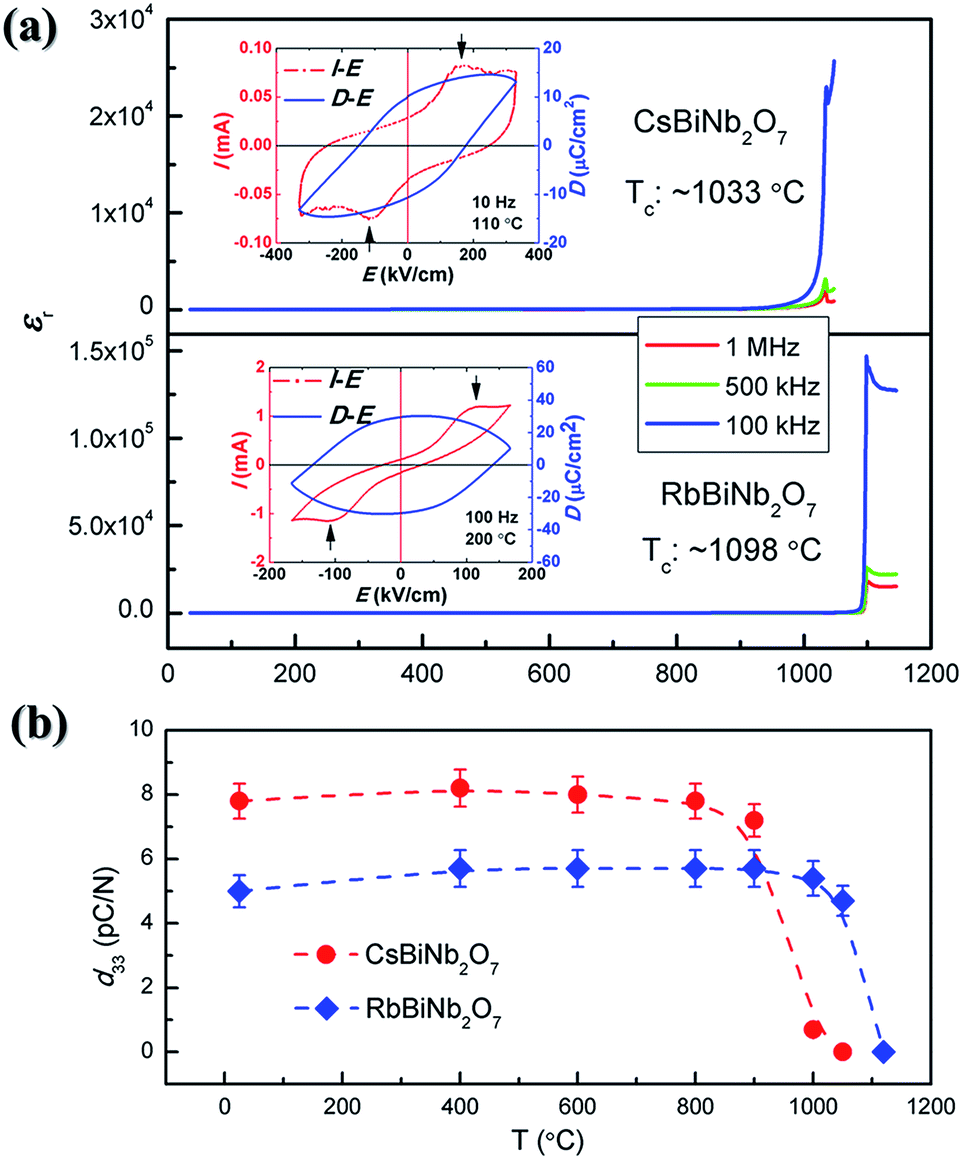 | ||
| Fig. 4 (a) Temperature dependence of dielectric constant; insets: I–E and D–E hysteresis loops; (b) thermal depoling results. | ||
CsBiNb2O7 and RbBiNb2O7 have similar polar orthorhombic structure P21am. Due to the off-centre displacements of A-site Bi ions and octahedral tilting of NbO6, a spontaneous polarization develops along their a-axis. Recently Benedek reported that the origin of ferroelectricity in polar oxides with Dion–Jacobson phases is induced by a combination of octahedral distortions and cation ordering.18 The macroscopic polarizations of CsBiNb2O7 and RbBiNb2O7 were both reported to be 48 μC cm−2 using symmetry principles, crystal chemical models, and first-principles calculations. Here the spontaneous polarization was calculated to be 43.8 μC cm−2 for CsBiNb2O7 and 47 μC cm−2 for RbBiNb2O7 according to Shimakawa's model,19,20 which is in good agreement with Benedek's report. The measured piezoelectric constant d33 at room temperature was 8 ± 0.5 pC N−1 for CsBiNb2O7 and 5 ± 0.5 pC N−1 for RbBiNb2O7. Fig. 4(b) shows the thermal depoling results for poled CsBiNb2O7 and RbBiNb2O7. All the samples poled at room temperature were annealed at different temperatures for 2 hours. Then their d33 values were measured at room temperature. For both CsBiNb2O7 and RbBiNb2O7, their d33 values are very stable with increasing depoling temperature. The d33 starts to drop when the depoling temperature is close to Tc and tends to zero above Tc.
In summary, highly textured 2-layer Dion–Jacobson ceramics ABiNb2O7 (A = Rb and Cs) were prepared by one-step spark plasma sintering with pressure due to their layered crystal structure, which was demonstrated using XRD. High resolution TEM showed well ordered (0 0 1) lattice planes. Striped ferroelectric domains were observed using PFM. The ferroelectricity and piezoelectricity of CsBiNb2O7 has been demonstrated for the first time. The Tc of RbBiNb2O7 and CsBiNb2O7 are 1098 ± 5 and 1033 ± 5 °C, respectively. The piezoelectric constant of RbBiNb2O7 and CsBiNb2O7 were approximately 5 and 8 pC N−1. Thermal depoling studies confirmed the Tc measurements and the stability of the piezoelectricity.
Acknowledgements
The Innovation Research and Development Programme of the Department of Business, Innovation and Skills, UK is acknowledged. Chen thanks China Scholarship Council (CSC) for supporting his PhD studies.Notes and references
- F. Lichtenberg, A. Herrnberger and K. Wiedenmann, Prog. Solid State Chem., 2008, 36, 253 CrossRef CAS PubMed.
- F. Lichtenberg, A. Herrnberger, K. Wiedenmann and J. Mannhart, Prog. Solid State Chem., 2001, 29, 1 CrossRef CAS.
- S. Zhang and F. Yu, J. Am. Ceram. Soc., 2011, 94, 3153 CrossRef CAS PubMed.
- M. Nyman, M. A. Rodriguez, L. E. S. Rohwer, J. E. Martin, M. Waller and F. E. Osterloh, Chem. Mater., 2009, 21, 4731 CrossRef CAS.
- T. Wang, C. N. Henderson, T. I. Draskovic and T. E. Mallouk, Chem. Mater., 2013, 26, 898 CrossRef.
- D. G. Cahill, A. Melville, D. G. Schlom and M. A. Zurbuchen, Appl. Phys. Lett., 2010, 96, 121903 CrossRef PubMed.
- T. Ukita, Y. Hirose, S. Ohno, K. Hatabayashi, T. Fukumura and T. Hasegawa, J. Appl. Phys., 2012, 111, 07D909 CrossRef PubMed.
- I. Levin and L. A. Bendersky, Acta Crystallogr., Sect. B: Struct. Sci., 1999, 55, 853 CrossRef PubMed.
- S. Nanamatsu, M. Kimura, K. Doi, S. Matsushita and N. Yamada, Ferroelectrics, 1974, 8, 511 CrossRef CAS.
- H. Yan, H. Ning, Y. Kan, P. Wang and M. J. Reece, J. Am. Ceram. Soc., 2009, 92, 2270 CrossRef CAS PubMed.
- H. Ning, H. Yan and M. J. Reece, J. Am. Ceram. Soc., 2010, 93, 1409 CAS.
- M. A. Subramanian, J. Gopalakrishnan and A. W. Sleight, Mater. Res. Bull., 1988, 23, 837 CrossRef CAS.
- A. Snedden, K. S. Knight and P. Lightfoot, J. Solid State Chem., 2003, 173, 309 CrossRef CAS.
- C. J. Fennie and K. M. Rabe, Appl. Phys. Lett., 2006, 88, 262902 CrossRef PubMed.
- R. J. Goff, D. Keeble, P. A. Thomas, C. Ritter, F. D. Morrison and P. Lightfoot, Chem. Mater., 2009, 21, 1296 CrossRef CAS.
- B.-W. Li, M. Osada, T. C. Ozawa and T. Sasaki, Chem. Mater., 2012, 24, 3111 CrossRef CAS.
- P. K. Gallagher, H. M. O'Bryan and C. D. Brandle, Thermochim. Acta, 1988, 133, 1 CrossRef CAS.
- N. A. Benedek, Inorg. Chem., 2014, 53, 3769 CrossRef CAS PubMed.
- H. Yan, H. Zhang, R. Ubic, M. J. Reece, J. Liu, Z. Shen and Z. Zhang, Adv. Mater., 2005, 17, 1261 CrossRef CAS.
- Y. Shimakawa, Y. Kubo, Y. Nakagawa, S. Goto, T. Kamiyama, H. Asano and F. Izumi, Phys. Rev. B: Condens. Matter Mater. Phys., 2000, 61, 6559 CrossRef CAS.
Footnote |
| † Electronic supplementary information (ESI) available: Experimental procedure, XRD results of sintered ceramics, PFM of RbBiNb2O7. See DOI: 10.1039/c4tc02136c |
| This journal is © The Royal Society of Chemistry 2015 |