DOI:
10.1039/C4TC01949K
(Communication)
J. Mater. Chem. C, 2015,
3, 26-32
Efficient polymer solar cells fabricated from solvent processing additive solution
Received
29th August 2014
, Accepted 28th October 2014
First published on 30th October 2014
Abstract
In this study, we investigate the device performance of bulk heterojunction (BHJ) polymer solar cells (PSCs) fabricated from pristine chlorobenzene (CB) solution, CB solutions with different concentrations of solvent processing additive, chloronaphthalene (CN) which has a high boiling point temperature, and pristine CN solution. An efficiency of 7.12% is observed from PSCs processed from pristine CN solution as compared with 4.01% of that from pristine CB solution. The correlation between the efficiency of PSCs with the concentrations of CN was systematically studied by absorption spectra, atomic force microscopy and cross-section transmission electron microscopy images, wide angle X-ray diffraction and grazing incidence small angle X-ray patterns of BHJ active layers and impedance spectroscopies of BHJ PSCs. It was found that the addition of CN into CB solution does not affect the crystallization or the molecular packing of the donor polymer in BHJ layers, but it changes the film morphology of the BHJ layers. The phase separation between the donor polymer and fullerene derivatives was reduced and BHJ layers were redistributed as the concentration of CN is increased in CB solutions. As a result, increased ratios of the donor polymer to fullerene derivatives, and high hole mobilities of the donor polymer in BHJ layers were obtained for the resultant films. Consequently, a high efficiency was observed from PSCs processed from CN solution rather than from CB solution. Our findings provide a method to approach highly efficient PSCs.
1. Introduction
Low-cost, solution-processed bulk heterojunction (BHJ) polymer solar cells (PSCs) have been developed as a promising alternative to inorganic-based photovoltaic cells.1–5 In PSCs, the BHJ active layer was solution-processed from the mixture of conjugated polymers and fullerene derivatives in a common solvent. Thus, the properties of the solvent, such as the solubility of the solvent to the polymers or the fullerene derivatives and the boiling-point (b. p.) temperature of the solvent, play a critical role in defining the film morphology of the BHJ active layer.6–11 In order to manipulate the film morphology of the BHJ active layer, one simple strategy is to cast the film from the BHJ composite in a common solvent mixed with a small amount of solvent processing additive which has a high b. p. temperature.6–11 With the addition of such solvent processing additives, the polymers and/or the fullerene derivatives will remain in the solution state for a long period before the solid state BHJ film is formed, so the polymer and the fullerene derivative domains will aggregate into an optimized size, which is favorable for charge carriers being separated and transported through the BHJ layer, resulting in high efficiency of BHJ PSCs.3 However, it was demonstrated that only a moderate amount of solvent additives will result in the expected film morphology, hence increased device performance.10,12–14 The addition of such solvent processing additives could introduce high surface energy to the mixture solution resulting in the dewetting process during film formation,13 and deteriorates the formation of the BHJ active layer when the polymers are easy to crystallize.13
In this study, we report the efficient PSCs fabricated from solvent processing additive chloronaphthalene (CN, b. p. 259 °C) solution. The power conversion efficiencies (PCEs) of PSCs fabricated using poly[4,8-bis[(2-ethylhexyl)oxy]benzo[1,2-b:4,5-b′]dithiophene-2,6-diyl][3-fluoro-2-[(2-ethylhexyl)carbonyl]thieno[3,4-b]-thiophenediyl] (PTB7) blended with [6,6]-phenyl-C71-butyric acid methyl ester (PC71BM) were increased to 7.12% from 4.01% as the PTB7:PC71BM BHJ composites processed from CN solution as compared to that from chlorobenzene (CB), with a b. p. of 131 °C. It was found that the additional CN in CB solutions could affect the film formation process hence to modify the film morphology of PTB7:PC71BM BHJ active layers, which result in an enhanced hole mobility of PTB7 in PTB7:PC71BM BHJ active layers and enhanced light capture by PTB7 due to the increased composition ratios of PTB7 to PC71BM in the resultant layers, and reduced internal charge transport resistances in PSCs. To the best of our knowledge, this is the first report that a high b. p. solvent is used as the solvent for approaching highly efficient PSCs.
2. Experimental
Materials
PTB7 was purchased from One-Material Inc. and PC71BM was purchased from Solenne. Both of the materials were used as received without further purification. PEDOT:PSS (poly(3,4-ethylenedioxythiophene):polystyrene sulfonate) (Clevios™ HTL Solar) was purchased from Heraeus and used as received. The solvents, CB (anhydrous, 99.8%) and CN (technique grade) were purchased from Sigma-Aldrich and used without further purification. Aluminum (99.99%) was purchased from Sigma-Aldrich. The molybdenum oxide powder was purchased from Alfa Aesar.
Absorption spectroscopy
The absorption spectra of PTB7:PC71BM films, which are cast from CB solutions with different concentrations of CN on top of PEDOT:PSS coated on ITO substrates were recorded by using a HP 8453 UV-vis spectrophotometer. The absorption spectra of the PTB7 thin layer cast from pristine CB and pristine CN solutions and the PC71BM thin layer cast from CB solution were also recorded by using a HP 8453 UV-vis spectrophotometer.
Atomic force microscopy (AFM) measurement
AFM images were taken on a Nano-Scope NS3A system (Digital Instrument) to investigate the surface topology of PTB7:PC71BM films cast from CB solutions with different concentrations of CN.
Impedance spectroscopy (IS) measurement
IS was carried out using a HP 4194A Impedance/gain-phase analyzer. All the devices were operated under dark conditions with an oscillating voltage of 10 mV and frequency of 5 Hz to 100 kHz. All PSCs were held at their respective open circuit potentials obtained from the J–V measurements, while the IS spectra were recorded.
Cross-section transmission electron microscopy (TEM)
The PTB7:PC71BM films were spin coated from CB solutions with different concentrations of CN. A carbon dye was deposited on these films as a signal indicator. Cross-section TEM images of the films were captured by using a FEI-Philips scanning transmission electron microscope, Model Tecnai T12T/STEM.
Wide angle X-ray diffraction (WAXRD)
WAXRD patterns of BHJ films deposited from pristine CB, CB with different concentrations of CN and pristine CN were obtained by using a Bruker AXS Dimension D8 X-ray System.
Grazing incidence small angle X-ray scattering (GISAXS) measurement
The thin films of BHJ composites were spin-coated on a silicon wafer from pristine CB, CB with 50% CN and pristine CN solution. The fabrication process for the thin films is the same as that used for the device fabrication. GISAXS was carried out in a beamline 8-ID-E, Advanced Photon Source, Argonne National Lab.
Film thickness measurement
The thickness of PTB7:PC71BM films fabricated from CB solutions with different concentrations of CN was characterized by using a Dektak 150 surface profilometer with a scan rate of 0.06 mm s−1.
Device fabrication and characterization
A conventional PSC with a device structure of ITO/PEDOT:PSS/PTB7:PC71BM/Al was fabricated and characterized, where ITO is indium tin oxide and Al is aluminum. The ITO substrates were ultrasonicated in acetone, detergent, deionized water and isopropanol subsequently and dried in an oven before device fabrication. An ∼30 nm thick PEDOT:PSS layer was formed by spin coating the precursor solution on the pre-cleaned ITO substrates and thermal annealing at 150 °C for 10 min. ∼120 nm active layers were spin-cast from PTB7![[thin space (1/6-em)]](https://www.rsc.org/images/entities/char_2009.gif) :PC71BM (1:1.5 weight ratio, 1 v/v%) in CB solutions with different concentrations of CN in a nitrogen glovebox. ∼100 nm of aluminum (Al) was thermally deposited on the PTB7:PC71BM active layer through a shadow mask in a vacuum of 2 × 10⁻⁶ mbar. The device area is 0.16 cm2. The PSCs were characterized by using a Newport Air Mass 1.5 Global (AM 1.5G) full spectrum solar simulator with irradiation of 100 mW m−2 calibrated by standard silicon solar cells. The current density–voltage (J–V) characteristics of PSCs were measured using a Keithley 2400 source meter. Note that the active layers spin coated from solution with high concentrations of CN and pristine CN were dried in a vacuum over 1 h before Al electrode thermal deposition.
:PC71BM (1:1.5 weight ratio, 1 v/v%) in CB solutions with different concentrations of CN in a nitrogen glovebox. ∼100 nm of aluminum (Al) was thermally deposited on the PTB7:PC71BM active layer through a shadow mask in a vacuum of 2 × 10⁻⁶ mbar. The device area is 0.16 cm2. The PSCs were characterized by using a Newport Air Mass 1.5 Global (AM 1.5G) full spectrum solar simulator with irradiation of 100 mW m−2 calibrated by standard silicon solar cells. The current density–voltage (J–V) characteristics of PSCs were measured using a Keithley 2400 source meter. Note that the active layers spin coated from solution with high concentrations of CN and pristine CN were dried in a vacuum over 1 h before Al electrode thermal deposition.
External quantum efficiency (EQE) measurement
The EQE was measured through the EQE measurement setup (DSR100UV-B) in use at ESTI for cells and mini-modules. A 300 W steady-state xenon lamp provides the source light. After collecting the EQE data, the software also integrates the date with the AM1.5G spectrum and gives the calculated JSC value.
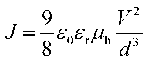
Hole mobility
The hole mobilities of PTB7 in active layers were estimated by the space charge limited current (SCLC) method based on the J–V characteristics of the diode with a structure of ITO/PEDOT:PSS/PTB7:PC71BM/MoOX/Ag/Al. The J–V characteristics of the diodes were measured by using a Keithley 2400 source meter. The hole mobilities of PTB7 in different active layers were estimated by the equation:  , where J is the current density, ε0 is the permittivity of free space, 8.85 × 10⁻¹² F m−1 and εr is the relative permittivity of PTB7 which generally was estimated to be 3, V is the applied voltage and d is the thickness of the active layers.
3. Results and discussion
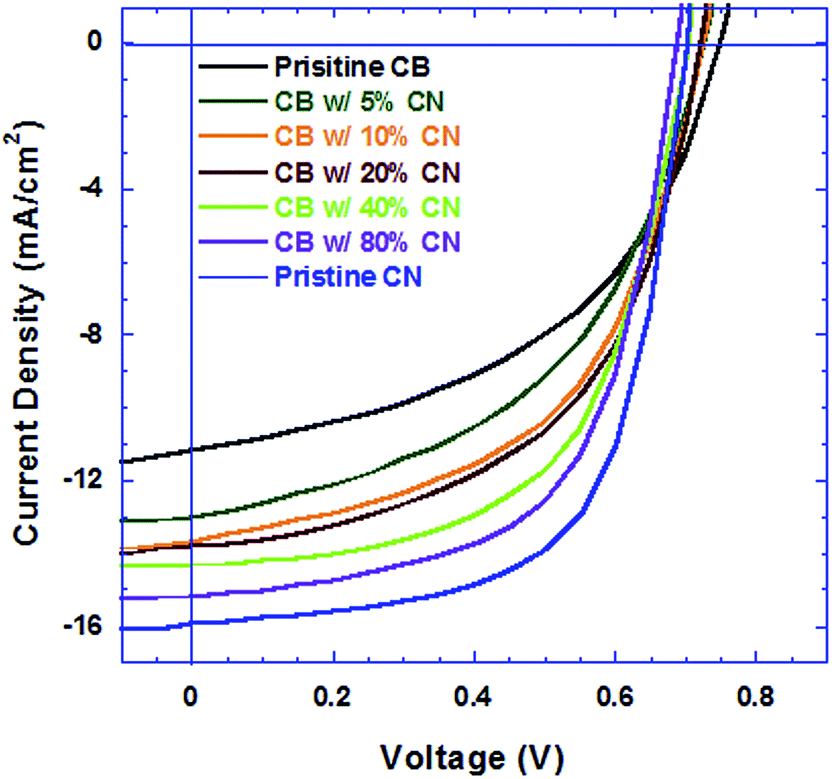
The current density versus voltage (J–V) characteristics of PSCs are shown in Fig. 1. Table 1 summarizes the average device performance parameters. The PSCs based on the PTB7:PC71BM BHJ composite processed from pristine CB solution exhibit an open-circuit voltage (VOC) of 0.75 V, a short-circuit current (JSC) of 11.15 mA cm−2, a fill factor (FF) of 48% and a corresponding PCE of 4.01%. The PSCs based on the PTB7:PC71BM BHJ composite processed from CB solutions with different concentrations of CN exhibit the same VOC, but with both increased JSC and FF, consequently, enhanced PCEs. The PSCs based on the PTB7:PC71BM BHJ composite processed from pristine CN solution exhibit a JSC of 15.90 mA cm−2, a FF of 63.9% and a corresponding enhanced PCE of 7.12%. Over 20 identical devices with the active layer fabricated from pristine CB, CB with different concentrations of CN and pristine CN were fabricated for the statistical study. The deviations in PCEs of devices are less than 5%. The PCEs from the PSCs based on the PTB7:PC71BM BHJ composite processed from CB solutions with increasing concentrations of CN are significantly higher than that from pristine CB solution and the PCE of the PSCs based on the PTB7:PC71BM BHJ composite processed from pristine CN solution is nearly twice higher than that from pristine CB. These results demonstrate that high b. p. solvent processing additive CN has a significant effect on the performance of PSCs.
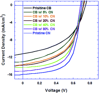 |
| | Fig. 1
J–V characteristics of PSCs processed from different solutions. | |
Table 1 Device performance of PSCsa
| Device |
V
OC (V) |
J
SC (mA cm−2) |
FF (%) |
PCE (%) |
|
Device parameters with each composition shown in the table are mean values over 20 devices. The deviations in device performance are less than 5%.
|
| Pristine CB |
0.75 |
11.20 ± 0.30 |
48.0 ± 1.0 |
4.01 ± 0.05 |
| CB w/5% CN |
0.72 |
13.00 ± 0.11 |
50.3 ± 0.8 |
4.58 ± 0.11 |
| CB w/10% CN |
0.72 |
13.65 ± 0.03 |
54.2 ± 0.1 |
5.18 ± 0.15 |
| CB w/20% CN |
0.71 |
13.80 ± 0.20 |
55.1 ± 1.1 |
5.40 ± 0.21 |
| CB w/40% CN |
0.70 |
14.32 ± 0.05 |
58.5 ± 0.2 |
5.86 ± 0.05 |
| CB w/80% CN |
0.69 |
15.17 ± 0.11 |
59.1 ± 1.2 |
6.27 ± 0.09 |
| Pristine CN |
0.70 |
15.92 ± 0.16 |
63.9 ± 0.1 |
7.12 ± 0.07 |
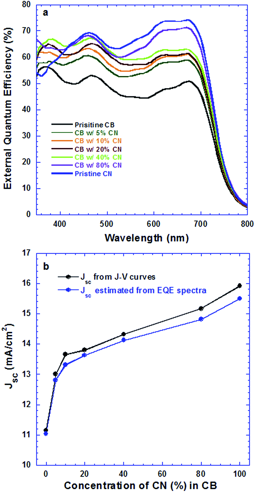
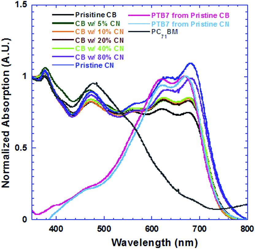
Fig. 2a presents EQE spectra of PSCs based on the PTB7:PC71BM BHJ composite processed from pristine CB, CB solutions with different concentrations of CN and pristine CN. The JSC values estimated from the EQE spectra of all PSCs and the JSC values observed from J–V characteristics are presented in Fig. 2b. It is clear that the estimated JSC values are consistent with the measured JSC values. Interestingly, the PSCs based on the PTB7:PC71BM BHJ composite processed from CB solutions with different concentrations of CN possess different profiles of EQE spectra. As the concentrations of CN are increased, the EQE intensities at wavelengths ranging from 550 nm to 720 nm are increased, but those at wavelengths ranging from 400 nm to 550 nm are decreased. In order to understand these changes, the absorption spectra of PTB7:PC71BM BHJ films cast from pristine CB solution, CB solutions mixed with different concentrations of CN and pristine CN solution were measured under the same conditions. The normalized absorption spectra of these films are presented in Fig. 3. Both absorption spectra of the pristine PTB7 film and pristine PC71BM are also presented in Fig. 3 for comparison studies. The EQE spectra of PSCs are consistent with the absorption spectra of BHJ active layers. It is clear that the enhanced EQE intensities at wavelengths ranging from 550 nm to 700 nm are contributed from PTB7 (ref. 15) and decreased EQE intensities at wavelengths ranging from 400 nm to 550 nm are assigned to PC71BM.16 The differences in both EQE profiles of PSCs and absorption spectra of BHJ thin films indicate that the film morphologies of BHJ active layers processed from pristine CB solution, CB solutions mixed with different concentrations of CN, and pristine CN are different; the component ratios of PTB7 to PC71BM in the resultant layers are increased as the concentrations of CN are increased in CB solutions.
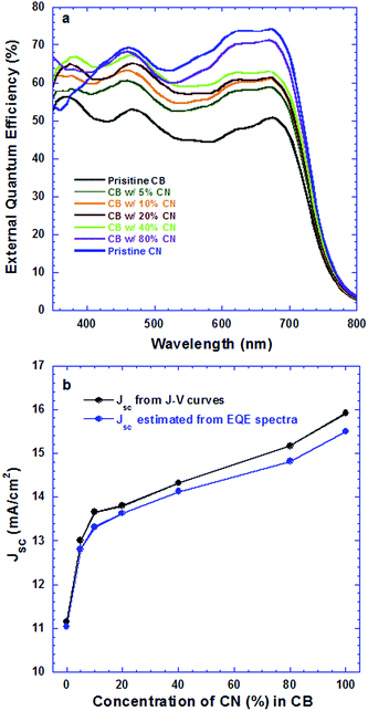 |
| | Fig. 2 (a) EQE spectra of PSCs processed from different solutions and (b) JSC from both J–V curves and EQE correlated with concentrations of CN in CB solutions. | |
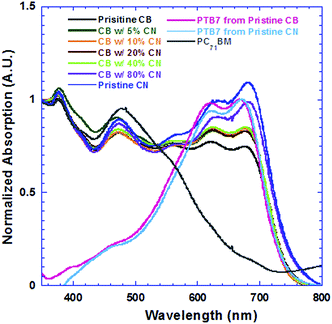 |
| | Fig. 3 Absorption spectra of active layers deposited from precursors with different concentrations of CN, PTB7 thin films deposited from pristine CB and pristine CN, and PC71BM thin film. | |
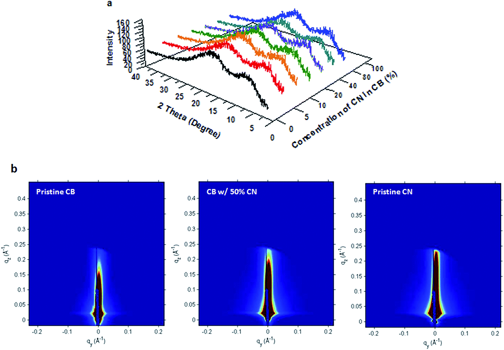
Both WAXRD and GISAX are used to characterize the molecular structures of PTB7 in PTB7:PC71BM BHJ thin films. The WAXRD patterns of PTB7:PC71BM BHJ layers are shown in Fig. 4a. All peaks are located in the same position, with no significant difference in the peak intensities, indicating that there is no obvious change in the molecular packing of PTB7.17–19 The GISAX patterns of PTB7:PC71BM films as shown in Fig. 4b are also the same; PTB7 does not show any face-on or edge-on packing in any films, suggesting that PTB7 is hard to crystallize.20 Thus WAXRD and GISAX studies indicate that the molecular structures of PTB7 in all PTB7:PC71BM films are the same and no effect of CN on the molecular packing of PTB7 is observed.
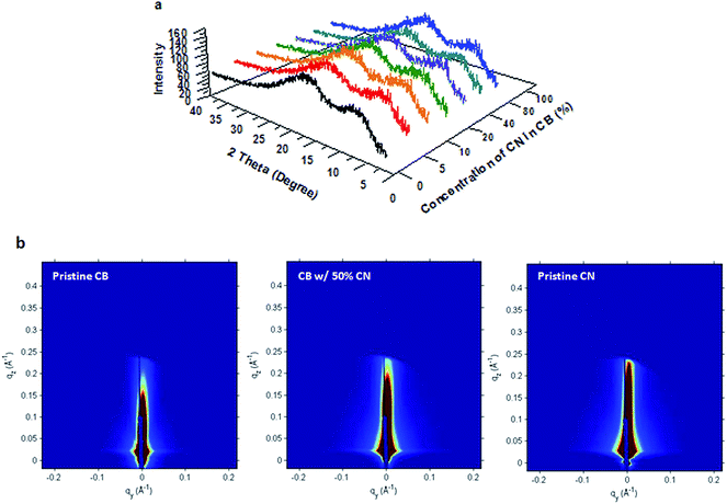 |
| | Fig. 4 (a) Wide angle X-ray diffraction pattern of BHJ layers processed from CB solutions with different concentrations of CN; (b) GISAX diffraction patterns of BHJ layers processed from pristine CB solution, CB solution with 50% CN and pristine CN solution. | |
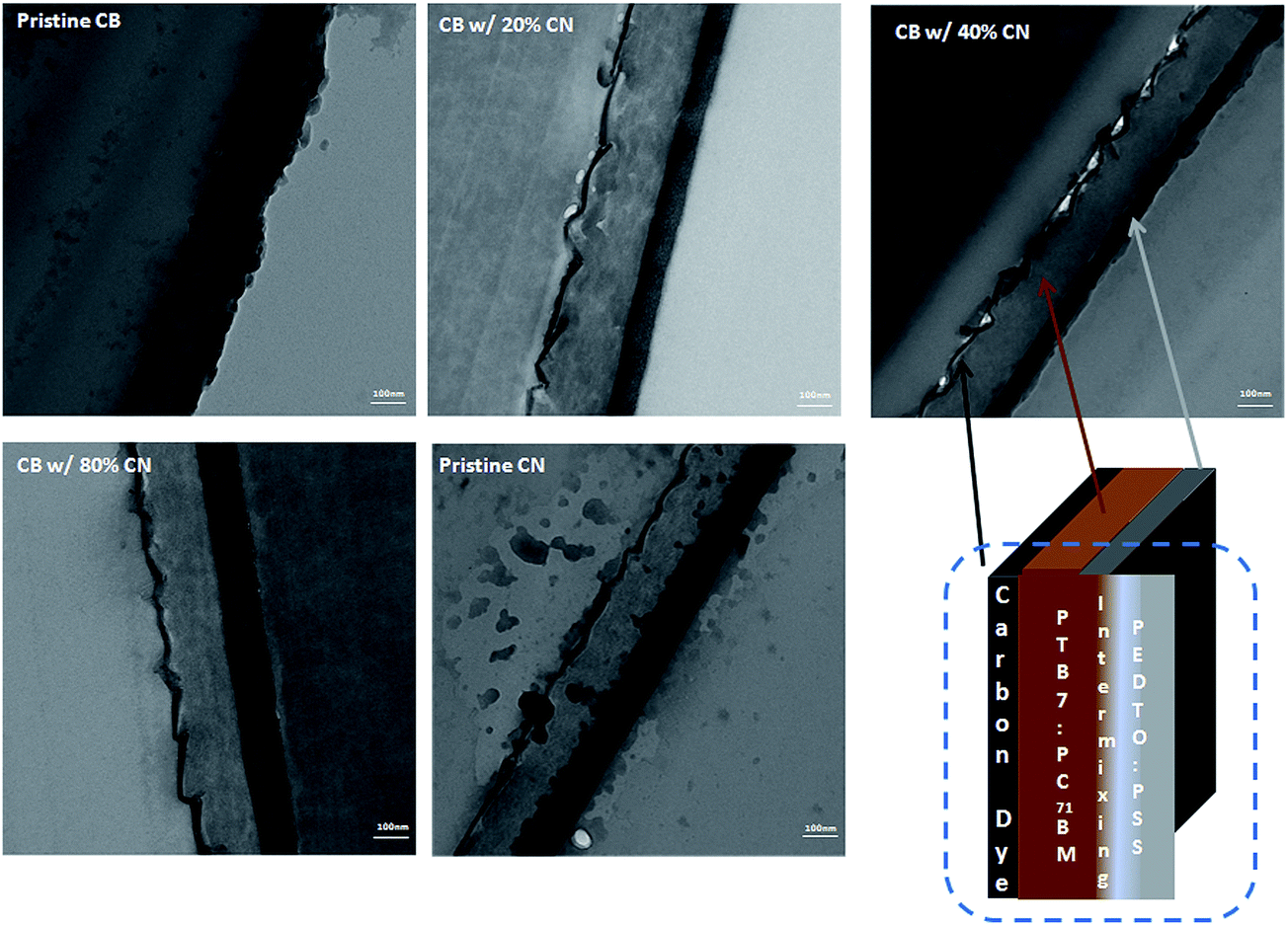
In order to further understand the underlying changes in both absorption spectra and EQE profiles, cross-section TEM was carried out to investigate the film morphology of the PTB7:PC71BM BHJ composite. Fig. 5 presents the cross-section TEM images of PTB7:PC71BM BHJ films processed from pristine CB solution, CB solutions with different concentrations of CN, and pristine CN. In the cross-section TEM images of PTB7:PC71BM/PEDOT:PSS/ITO/glass, where the PTB7:PC71BM BHJ composite is processed from pristine CB solution, the light layer is the PTB7:PC71BM active layer and the dark layer underneath the PTB7:PC71BM layer is the PEDOT:PSS layer.3,21 The thickness of the PEDOT:PSS layer underneath the PTB7:PC71BM layer is ∼30 nm, which is consistent with the measured thickness of the PEDOT:PSS layer (see the Experimental section). It was found that the thickness of the dark layer is increased as the PTB7:PC71BM BHJ composite is processed from the CB solutions with increased concentrations of CN. For instance, the thickness of the dark layer is 48 nm as the PTB7:PC71BM BHJ composite is processed from the CB solution with 40% of CN. The thickness of the dark layer is increased to 86 nm as the PTB7:PC71BM BHJ composite is processed from pristine CN solution. All these results demonstrate that the PTB7:PC71BM BHJ layer is re-distributed to the PCBM-rich (n-type layer) layer, PTB7:PC71BM BHJ layer (intrinsic layer) and PTB7-rich layer (p-type layer).9,11 The PTB7-rich layer is on top of the PEDOT:PSS layer.9,11 The re-distribution of the PTB7:PC71BM BHJ layer into the n–i–p structure would benefit the charge carrier to be transported into the respective electrodes.11,22–24 In order to verify this hypothesis, the hole-only devices were fabricated and characterized to investigate the hole mobility of PTB7 in the PTB7:PC71BM BHJ layer. The hole mobilities of PTB7 from PTB7:PC71BM BHJ layers processed from pristine CB solution, CB solutions with different concentrations of CN, and pristine CN solution are summarized in Table 2. The hole mobility of PTB7 from the PTB7:PC71BM BHJ layer processed from pristine CB solution is 3.94 × 10⁻⁴ cm2 V−1 s−1, while the hole mobilities of PTB7 from PTB7:PC71BM BHJ layers are increased as PTB7:PC71BM BHJ layers are processed from CB solutions with increased concentrations of CN. The hole mobility of PTB7 from the PTB7:PC71BM BHJ layer processed from pristine CN solution is 10.83 × 10⁻⁴ cm2 V−1 s−1, which is more than two times higher than that processed from pristine CB solution. These results confirm our hypothesis from TEM images of PTB7:PC71BM BHJ layers that hole transport could be facilitated in PTB7:PC71BM BHJ layers processed from CB solutions with increased concentrations of CN. The thicknesses of the active layers cast from pristine CB, the CB solutions with different concentrations of CN and pristine CN are from 175 ± 10 nm.
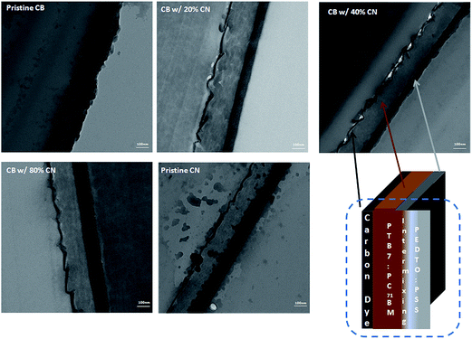 |
| | Fig. 5 Cross-sectional TEM images of BHJ/PEDOT:PSS layers where BHJ layers processed from CB solutions with different concentrations of CN. | |
Table 2 Hole mobilities of PTB7 in the BHJ layers
| BHJ layers processed from different solutions |
μ
h of PTB7 (cm2 V−1 s−1) |
| Pristine CB |
3.94 × 10⁻⁴ |
| CB w/5% CN |
4.67 × 10⁻⁴ |
| CB w/10% CN |
5.37 × 10⁻⁴ |
| CB w/20% CN |
5.80 × 10⁻⁴ |
| CB w/40% CN |
6.41 × 10⁻⁴ |
| CB w/80% CN |
7.46 × 10⁻⁴ |
| Pristine CN |
10.83 × 10⁻⁴ |
The film morphology of PTB7:PC71BM BHJ layers processed from different solutions was investigated by AFM. Fig. 6 presents the AFM height images of PTB7:PC71BM BHJ layers. It was found both the sizes of the polymer domain and fullerene aggregation are reduced along with the increased concentrations of CN in CB solutions. The reduced polymer domain and fullerene aggregation would result in a moderate phase separation, which facilitates charge carriers to be separated and transported within the BHJ layer.10,25,26
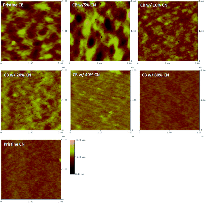 |
| | Fig. 6 AFM height images of BHJ layers processed from CB solutions with different concentrations of CN. | |
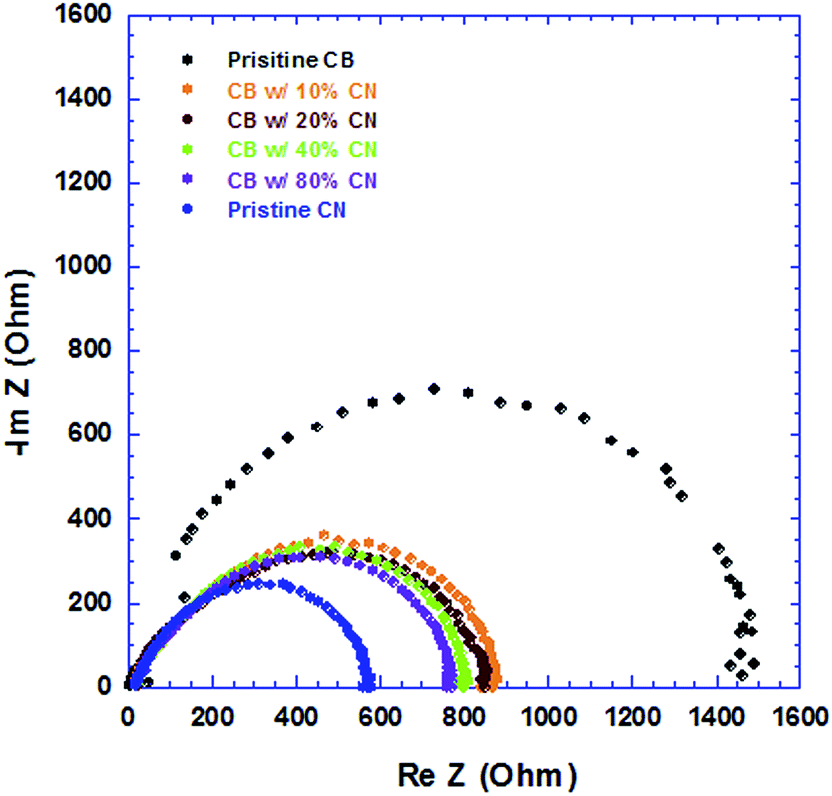
IS is carried out to investigate the detailed electrical properties of devices, which cannot be observed by direct current measurements. The internal resistance of the PSCs is composed of the sheet resistance (RSH) of the electrodes, and the charge-transport resistance (RCT) at the BHJ/electrode interfaces and inside the BHJ active layer. Since all the electrodes, ITO anode and Al cathode are the same for all PSCs, the sheet resistance of all PSCs should be the same. Thus the changes in the internal resistance originate from inside the BHJ active layers which are processed from CB solutions with different concentrations of CN. Fig. 7 displays the Nyquist plot of all PSCs. The internal resistance gradually reduced from 1450 Ω, 879 Ω, 830 Ω, 800 Ω, 760 Ω to 550 Ω, for the PSCs processed from pristine CB solution, CB solutions with 10%, 20%, 40%, 80% CN, and pristine CN solution, respectively. The decreased internal resistance further indicates that the film morphology of PTB7:PC71BM BHJ layers was affected by the incorporation of CN with CB solutions, which is in good agreement with the observation from cross-section TEM images. Furthermore, the decreased internal resistance would facilitate the charge transport in PSCs and the PSCs with high JSC and PEC are anticipated.27,28
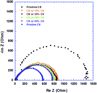 |
| | Fig. 7 Nyquist plot of PSCs where BHJ layers processed from CB solutions with different concentrations of CN. | |
4. Conclusions
In conclusion, we have reported efficient PSCs fabricated from CB solution with high boiling-point temperature solvent additive CN. We found that the addition of CN into CB solution does not affect the crystallization or the molecular packing of PTB7 in the PTB7:PC71BM BHJ layer, but it changes the film morphology of the PTB7:PC71BM BHJ layers. The phase separation between PTB7 and PC71BM was reduced and PTB7:PC71BM BHJ layers were redistributed as the concentration of CN is increased in CB solutions. As a result, an increased ratio of PTB7 to PC71BM and high hole mobility of PTB7 in PTB7:PC71BM BHJ layers were obtained for the resultant films. Consequently, an efficiency of 7.12% was observed from PSCs processed from pristine CN solution as compared to 4.01% of that from PSCs processed from pristine CB solution.
Acknowledgements
The authors would like to thank NSF (1351785) for financial support. The use of the Advanced Photon Source was supported by the U.S. Department of Energy, Office of Science, Office of Basic Energy Sciences, under Contract DE-AC02-06CH11357. The authors thank Zhang Jiang and Joseph Strzalka for assistance with GISAXS measurements. X. W. Hu thanks the China Scholarship Council for the Joint Ph. D. program.
References
- N. S. Sariciftci, L. Smilowitz, A. J. Heeger and F. Wudl, Science, 1992, 258, 1474 CAS.
- H.-Y. Chen, J. H. Hou, S. Zhang, Y. Liang, G. Yang, Y. Yang, L. Yu, Y. Wu and G. Li, Nat. Photonics, 2009, 3, 649 CrossRef CAS.
- G. Li, R. Zhu and Y. Yang, Nat. Photonics, 2012, 6, 153 CrossRef CAS.
- G. Li, V. Shrotriya, J. Huang, Y. Yao, T. Moriarty, K. Emery and Y. Yang, Nat. Mater., 2005, 4, 864 CrossRef CAS.
- Y. J. Cheng, S. H. Yang and C. S. Hsu, Chem. Rev., 2009, 109, 5868 CrossRef CAS PubMed.
- X. Yang, J. Loos, S. C. Veenstra, W. J. H. Verhees, M. M. Wienk, J. M. Kroon, M. A. J. Michels and R. A. J. Janssen, Nano Lett., 2005, 5, 579 CrossRef CAS PubMed.
- H. Hoppe and N. S. Sariciftci, J. Mater. Chem., 2006, 16, 45 RSC.
- S. van Bavel, S. Veenstra and J. Loos, Macromol. Rapid Commun., 2010, 31, 1835 CrossRef CAS PubMed.
- L. M. Chen, Z. Hong, G. Li and Y. Yang, Adv. Mater., 2009, 21, 1434 CrossRef CAS.
- C. V. Hoven, X. D. Dang, R. C. Coffin, J. Peet, T.-Q. Nguyen and G. C. Bazan, Adv. Mater., 2010, 22, E63 CrossRef CAS PubMed.
- X. Guo, M. Zhang, W. Ma, L. Ye, S. Zhang, S. Liu, H. Ade, F. Huang and J. Hou, Adv. Mater., 2014, 26, 4043 CrossRef CAS PubMed.
- J. Peet, J. Y. Kim, N. E. Coates, W. L. Ma, D. Moses, A. J. Heeger and G. C. Bazan, Nat. Mater., 2007, 6, 497 CrossRef CAS PubMed.
- F.-C. Chen, H.-C. Tseng and C.-J. Ko, Appl. Phys. Lett., 2008, 92, 103316 CrossRef PubMed.
- X. Hu, M. Wang, F. Huang, X. Gong and Y. Cao, Synth. Met., 2013, 164, 1 CrossRef CAS PubMed.
- Y. Liang, Z. Xu, J. Xia, S. T. Tsai, Y. Wu, G. Li, C. Ray and L. Yu, Adv. Mater., 2010, 22, E135 CrossRef CAS PubMed.
- S. Pfuetzner, J. Meiss, S. Olthof, M. P. Hein, A. Petrich, L. Dunsch, K. Leo and M. Riede, Photonics for Solar Energy Systems III, Proc. SPIE, 2010, 7725, 77250E CrossRef PubMed.
- F. Liu, Y. Gu, J. W. Jung, W. H. Jo and T. P. Russell, J. Polym. Sci., Part B: Polym. Phys., 2012, 50, 1018 CrossRef CAS.
- M. A. Ruderer and P. M. Buschbaum, Soft Matter, 2011, 7, 5482 RSC.
- F. Liu, W. Zhao, J. R. Tumbleston, C. Wang, Y. Gu, D. Wang, A. L. Lriseno, H. Ade and T. P. Russell, Adv. Energy Mater., 2014, 4, 1301377 Search PubMed.
- J. R. Tumbleston, B. A. Collins, L. Yang, A. C. Stuart, E. Gann, W. Ma, W. You and H. Ade, Nat. Photonics, 2014, 8, 385 CrossRef CAS.
- H.-C. Liao, C.-C. Ho, C.-Y. Chang, M.-H. Jao, S. B. Darling and W.-F. Su, Mater. Today, 2013, 16, 326 CrossRef CAS PubMed.
- L. Zhang, X. Xing, L. Zheng, Z. Chen, L. Xiao, B. Qu and Q. Gong, Sci. Rep., 2014, 4, 5071 Search PubMed.
- A. Loiudice, A. Rizzo, G. Latini, C. Nobile, M. de Giorgi and G. Gigli, Sol. Energy Mater. Sol. Cells, 2012, 100, 147 CrossRef CAS PubMed.
- Y.-C. Huang, G. C. Welch, G. C. Bazan, M. L. Chabinyc and W. Su, Chem. Commun., 2012, 48, 7250 RSC.
- T. Xiao, H. Xu, G. Grancini, J. Mai, A. Petrozza, U.-S. Jeng, Y. Wang, X. Xin, Y. Lu, N. S. Choon, H. Xiao, B. S. Ong, X. Lu and N. Zhao, Sci. Rep., 2014, 4, 5211 Search PubMed.
- P. Dutta, Y. Xie, M. Kumar, M. Rathi, P. Ahrenkiel, D. Galipeau, Q. Qiao and V. Bommisetty, J. Photonics Energy, 2011, 1, 011124 CrossRef PubMed.
- H. Zhou, Y. Zhang, J. Seifter, S. D. Collins, C. Luo, G. C. Bazan, T. Q. Nguyen and A. J. Heeger, Adv. Mater., 2013, 25, 1646 CrossRef CAS PubMed.
- M. Knipper, J. Parisi, K. Coakley, C. Waldauf, C. J. Brabec and V. Dyakonov, Z. Naturforsch., 2007, 62, 490 CAS.
|
| This journal is © The Royal Society of Chemistry 2015 |

 , where J is the current density, ε0 is the permittivity of free space, 8.85 × 10⁻¹² F m−1 and εr is the relative permittivity of PTB7 which generally was estimated to be 3, V is the applied voltage and d is the thickness of the active layers.