
 Open Access Article
 This Open Access Article is licensed under a Creative Commons Attribution-Non Commercial 3.0 Unported Licence
Solvent vapor annealing on perylene-based organic solar cells†
Stefan
Grob
*a,
Andrew N.
Bartynski
b,
Andreas
Opitz
c,
Mark
Gruber
a,
Florian
Grassl
a,
Eduard
Meister
a,
Theresa
Linderl
a,
Ulrich
Hörmann
a,
Christopher
Lorch
d,
Ellen
Moons
e,
Frank
Schreiber
d,
Mark E.
Thompson
b and
Wolfgang
Brütting
*a
aInstitut für Physik, Universität Augsburg, Universitätsstraße 1, 86135 Augsburg, Germany. E-mail: stefan.grob@physik.uni-augsburg.de; wolfgang.bruetting@physik.uni-augsburg.de
bInstitut für Physik, Humboldt-Universität zu Berlin, Brook-Taylor-Straße 6, 12489 Berlin, Germany
cDepartment of Chemical Engineering, Department of Chemistry, University of Southern California, Los Angeles, California 90089, USA
dInstitut für Angewandte Physik, Universität Tübingen, Auf der Morgenstelle 10, 72076 Tübingen, Germany
eDepartment of Engineering and Physics, Karlstad University, SE-65188 Karlstad, Sweden
First published on 2nd July 2015
Abstract
Diindenoperylene (DIP) and tetraphenyldibenzoperiflanthene (DBP) are two commonly used donor materials in organic solar cell devices. Despite their structural similarities, DIP films are crystalline, exhibiting good charge and exciton transport, whereas DBP films are amorphous and have lower carrier mobility and a short exciton diffusion length. However, DBP reveals a distinctly higher absorption due to the lying orientation of its transition dipole moments. In this paper, we investigate the influence of solvent vapor annealing (SVA) on the solar cell performance of both materials. In general, SVA induces a partial re-solubilization of the material leading to enhanced crystallinity of the treated layer. For DBP, extended annealing times result in a strong aggregation of the molecules, creating inhomogeneous layers unfavorable for solar cells. However, in DIP cells, SVA leads to an increase in fill factor (FF) and also a slight increase in short-circuit current density (JSC) due to interface roughening. The best results are obtained by combining solvent vapor annealed DIP layers with strongly absorbing DBP and C70 on top. Through this device architecture, we obtain the same increase in FF in addition to a higher gain in JSC, elevating the power conversion efficiency by a factor of 1.2 to more than 4%.
I Introduction
During the past several years, research on small-molecule and polymer-based organic photovoltaic cells (OPVs) has led to a significant enhancement in power conversion efficiency (PCE) following various approaches, like cascades,1 plasmonic nanostructures2 and planar-mixed architectures.3 Thus, efficiencies greater than 9% have been achieved for small molecule single-junction cells4–6 and efficiencies even greater than 10% have been reported for tandem or triple-junction devices.7,8 These works have shown that there are numerous factors that influence the complex mechanisms occurring within an OPV during charge carrier generation which can cause an improvement of the efficiency. Of course, the choice of donor and acceptor materials is fundamental. Fullerenes like C60 and C70 are the most common acceptor materials in small-molecule OPVs yielding good results in combination with various donors and are also used in this study. In recent years, perylenes have attracted attention for use as donor materials. Tetraphenyldibenzoperiflanthene (DBP) has proven to be especially well suited for the fabrication of highly efficient OPVs3,8 due to its high absorption coefficient and despite its amorphous character. Also its crystalline counterpart diindenoperylene (DIP) has already been utilized successfully in organic solar cells.9–11 It offers good charge12 and exciton transport,13 but suffers from poor absorption due to unfavorable orientation of the optical transition dipole moment.14 Both perylenes will be used as donors within this work.Beside the choice of organic materials there are a couple of other factors which influence the performance of OPVs, as the process of charge generation is complex. The complexity can be illustrated by dividing the overall process into four sub-processes.15,16 First, photons are absorbed resulting in the formation of excitons. In the second step, the excitons diffuse to the donor–acceptor (D/A) interface. Exciton dissociation and the transfer of the separated charge carriers to donor and acceptor, respectively, represent the third sub-process. Finally, the free charge carriers are transported to the electrodes, where they are collected. Each of these four sub-processes can be characterized by a separate efficiency, labeled as the absorption efficiency ηAbs, the exciton diffusion efficiency ηED, the charge-transfer efficiency ηCT and the charge collection efficiency ηCC. The product of these partial efficiencies finally results in the external quantum efficiency ηEQE:
| ηEQE = ηAbsηEDηCTηCC. | (1) |
In this work, we investigate how solvent vapor annealing (SVA) leads to a modification of these individual sub-processes and quantify the impact SVA has on the overall performance of thermally evaporated, perylene-based organic solar cells. As the name suggests, SVA means the treatment of functional layers with solvent vapor while avoiding direct contact between the liquid solvent and the organic films. The film swells by taking up the solvent molecules of the vapor. As a result, the organic molecules become mobile and can rearrange leading to a higher structural order within the layer.17–20
An increased crystallinity is able to affect the efficiency of the first sub-process as ηAbs is, on the one hand, determined by the organic layer thickness. It has already been shown that enhanced crystallinity allows the use of thicker active layers without negatively impacting the fill factor.21 Furthermore, we clarify the influence of SVA on the second important factor determining ηAbs, the absorption strength of the utilized materials, which is mainly determined by the orientation of the molecules. For example, an upright standing arrangement of organic molecules inhibits strong coupling between the incident light and the transition dipole moment aligned along the long axis of the molecules and results in weak absorption. This is the case for the crystalline donor DIP with its molecules standing almost upright, tilted by an angle of ϕ ≈ 17° with respect to the surface normal.22 Conversely, a horizontal alignment of the molecules leads to strong coupling and as a consequence strong absorption. This is true for the second perylene, the amorphous DBP.23 SVA may provide a potential route to alter the orientation of molecules within the film, modifying their coupling with incident light and resulting in a change in ηAbs.
Moreover, all transport processes are expected to improve within the treated layer with increasing crystallinity. The efficiency of the diffusion of excitons ηED, as well as the transport of free charge carriers ηCC should increase. This implies that if the donor is annealed, the mobility of the holes rises, while a treatment of the acceptor should improve the electron transport. A measure for good transport is a low series resistance RS. To extract the series resistance of an organic solar cell, dark current characteristics can be analyzed. Although the physics behind it is not the same as in an inorganic p–n junction, it has been shown that the exponential part of the forward-bias characteristics can be described by a modified Shockley equation:24,25
 | (2) |
But not only the FF can be positively influenced, an improvement of ηED might also contribute to an increase of JSC as the second sub-process, the diffusion of excitons, also implies that excitons are able to diffuse to the D/A interface and do not recombine within the bulk. This is far from self-evident, considering that typical exciton diffusion lengths for organic materials are only a few nanometers,28,29 for example DBP exhibits an LD of 9 ± 3 nm.30 An alternative to increasing the exciton diffusion length is to increase the surface area of the D/A interface e.g. by co-evaporation, however, this results in a completely different concept, the bulk heterojunction (BHJ).31,32 Nevertheless, the interface area can also be increased in planar heterojunction (PHJ) devices, albeit on a smaller scale, by enlarging the roughness of the donor layer. As roughness is usually connected to crystallinity, SVA may also affect this parameter. Finally, the increase in the number of dissociated excitons leads to an increase in free charge carriers and thus a higher JSC.
The only process not influenced by SVA is the charge-transfer (CT) process, occurring at the D/A interface. As this dissociation process typically takes place over time scales of a few hundred femtoseconds or less,33–35 it is much shorter than any other competing process. Thus, as long as the nature of the D/A interface is not fundamentally changed, the charge-transfer efficiency approaches ηCT = 100%.36,37
II Solvent vapor annealing on amorphous donor DBP
In the treatment of organic layers with solvent vapor it is important to consider some correlations. First, the most suitable solvent has to be found for the material to be treated. For that reason, the solubility of DBP was evaluated in chlorobenzene, ortho-dichlorobenzene, chloroform, dichloromethane, toluene, xylene and tetrahydrofuran. Optical microscopy images show that chloroform yields the best results, as the DBP precipitates, which appear for all solvents, are surrounded by a purple-colored area as it is typical for (evaporated) DBP films. However, DBP does not show particularly good solubility in any of these solvents. In this work, all SVA treatments are carried out with chloroform. Beside the choice of a suitable solvent, it is important to find out an appropriate duration of the SVA treatment. This also depends largely on the treated material as well as on the layer thickness.Photovoltaic cells were fabricated on a transparent indium-tin oxide (ITO, 140 nm) electrode, covered with 45 nm of the poly(ethylenedioxythiophene):poly(styrenesulfonate) (PEDOT:PSS) derivative HIL1.3 to adjust the work function of the ITO anode for hole-selectivity. The thicknesses of the donor layers and the acceptor layers (C60, C70) are 30 nm and 45 nm, respectively. Exciton quenching at the organic–metal interface is suppressed by inserting 5 nm of bathocuproine (BCP) and the top electrode consists of 100 nm of aluminium (Al). For these samples, SVA was performed after evaporation of the donor material. As donor either crystalline DIP or amorphous DBP is used. Furthermore, solar cells were fabricated consisting of two donor layers with 15 nm DIP and 15 nm DBP, which were evaporated consecutively. In this case, DBP is the primary absorber while DIP acts as an exciton blocking layer, a concept which has already been established successfully.38,39 For these solar cells only the DIP layer is treated by use of SVA.
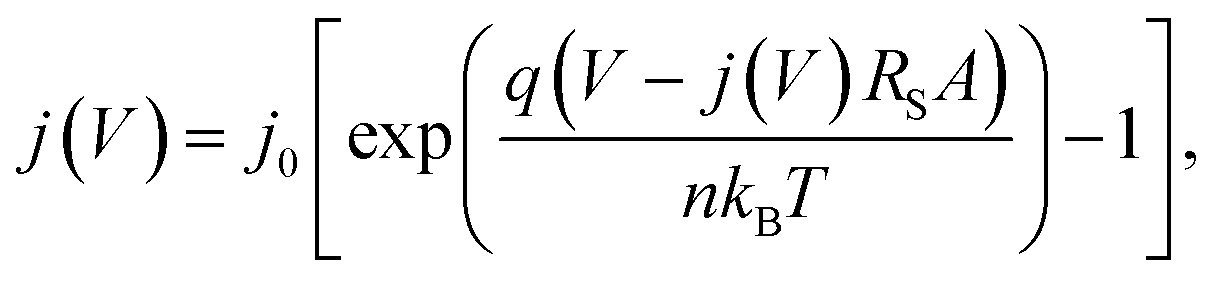
First of all, annealed DBP films were studied by optical microscopy. Inspection of an image taken from a sample annealed for 10 minutes under 20-fold magnification reveals that round DBP crystallites are formed with diameters of approximately 50 μm (Fig. 1). To investigate the crystallinity of the annealed layer, X-ray diffraction (XRD) measurements were performed. Initially, out-of-plane X-ray reflection (XRR) was measured, but just like the pristine layers no reflections, indicating a well-ordered crystalline structure, could be observed. Therefore, in-plane (grazing incident X-ray diffraction) measurements were recorded, but also in this configuration no peaks indicating DBP crystallinity are observable. The results of both, out-of-plane and in-plane measurements are shown in the ESI.† Other groups have already reported on more crystalline DBP, achieved through different techniques. Growing on a crystalline template38 or on a heated substrate40 as well as applying organic vapor phase deposition (OPVD) using a hot inert carrier gas21 were reported to result in DBP layers of higher order. However, in these cases the crystallinity could neither be visualized by means of XRD,38 nor via reflection high energy electron diffraction40 (RHEED) nor by selected area electron diffraction21 (SAED).
 | ||
| Fig. 1 Round crystallites formed in a 50 nm thick DBP-layer by annealing for 10 minutes in chloroform vapor. | ||
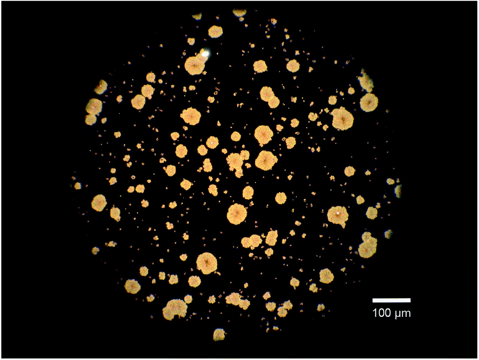
Next, we investigated the surface properties of 15 nm films of DBP annealed for various durations via AFM. There was no difference for layers growing either on ITO/HIL1.3 or on glass so the reorganization of the molecules is independent of the substrate. These layers were treated by SVA for 4, 8 and 12 minutes, respectively, and then compared with each other as well as with an untreated sample. As reported previously,23,40 the pristine DBP layer has an extremely smooth surface with a root-mean-square (RMS) roughness of merely RMS = 0.63 nm. However, SVA causes a strong aggregation of the DBP molecules. After 4 minutes of SVA treatment, the RMS roughness increases more than thirtyfold to 21.65 nm. Longer exposure times enhance this effect. For example, after 12 minutes of SVA the RMS roughness amounts to 39.8 nm with DBP islands up to 130 nm height and diameters of approximately 500 nm (Fig. 2).
 | ||
| Fig. 2 AFM images of a 15 nm DBP layer treated by SVA for (a) 0 minutes, (b) 4 minutes, (c) 8 minutes and (d) 12 minutes. | ||
The aggregation of molecules leads to a strong inhomogeneity within the DBP film, which is detrimental to the charge transport properties required for devices like photovoltaic cells.41 In addition to the negative effect on charge transport, the absorption also drops drastically. The change can already be seen with the naked eye, as the annealed layers became much more translucent, i.e. they absorb less. To quantify this observation, absorption measurements were performed. It can be seen that the correlation between SVA and the reduction of the absorption coefficient α depends on the annealing time (Fig. 3). There is hardly any change for the first two minutes of annealing followed by a slight decrease after four minutes. A more drastic change occurs after six minutes. At longer times of SVA no further change is visible. This correlates quite well with images taken by AFM, which also reveal negligible differences for eight and twelve minutes and an intermediate topography after four minutes (Fig. 2). Thus, we attribute the drop of absorption to a dewetting process of DBP leading to a decreased two-dimensional coverage of the substrate. Furthermore, the increasing absorption for wavelength higher than about 630 nm can most likely be attributed to scattering. This results from the extremely rough surface of crystalline DBP islands. As scattering is not detected in transmission nor reflection, it is included in the calculated absorption A = 1 − R − T. However, dewetting is not the only process which contributes to the absorption drop. Near edge X-ray absorption fine structure (NEXAFS) measurements reveal an additional change in molecular orientation. Measurements on pristine films yield a higher intensity of the 40° as compared to the 90° spectrum in the low energy region which is related to the transition from the C1s core level to the LUMO level. This reveals a more flat lying perylene core. After 4 minutes of SVA, however, no angular dependence appears any more. This is indicative of a reorientation process which has started, leading to an intermediate configuration, similar to the results obtained by AFM and absorption measurements. Further annealing yields a reversed angular dependence indicating a change of molecular orientation due to solvent vapor annealing (Fig. 4). These results indicate a more upright oriented perylene core and even more upright oriented phenyl rings. This leads to an unfavorable orientation of the transition dipole moment – which is aligned along the long axis of the molecule – and thus less absorption.
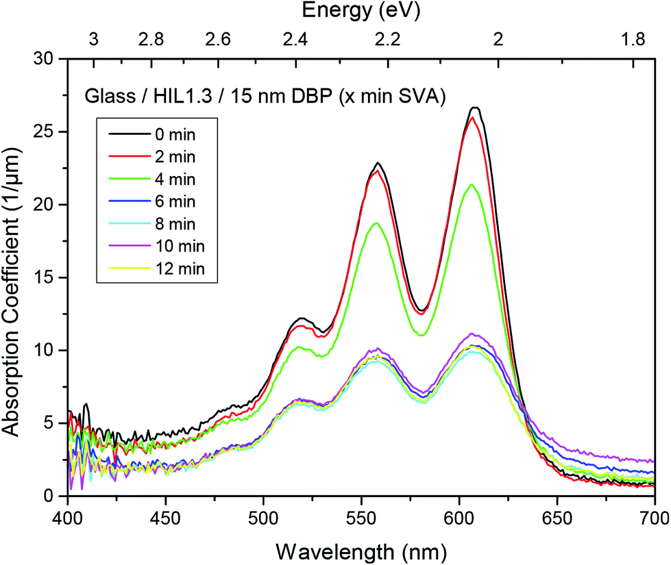 | ||
| Fig. 3 Correlation between SVA time and absorption drop of an annealed DBP layer. | ||
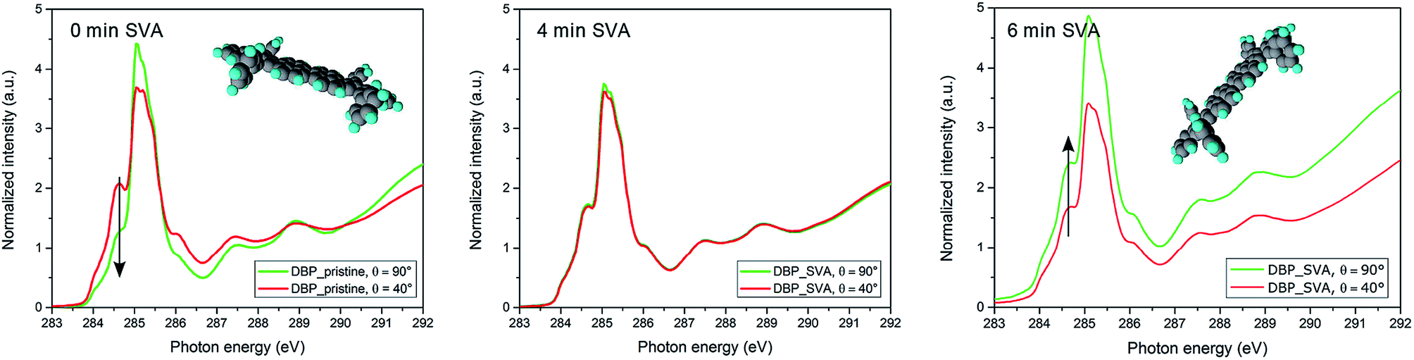 | ||
| Fig. 4 NEXAFS data of a 15 nm DBP film annealed for 0, 4 and 6 minutes at 40° and 90° angle of incidence (θ) of the X-ray photons. Comparing the data of the untreated sample and the sample annealed for 6 minutes a distinct change in dichroism is visible e.g. at about 284.6 eV. This indicates a change in molecular orientation from rather horizontal to more upright standing alignment. Additional data for θ = 30°, 55°, 70° confirm this trend, however, are omitted for clarity. The omitted data can be found in the ESI.† | ||
Evaluating the performance of solar cells fabricated with annealed DBP films confirms these problems. For elevated SVA times (t ≥ 6 min) all relevant values diminish. The decreased absorption leads to a smaller JSC, the fill factor declines due to poor transport and the open-circuit voltage (VOC) is reduced by enhanced recombination as the strong DBP aggregation leads to the appearance of pinholes limiting VOC.42 The origin of the loss in JSC can clearly be seen in the IPCE curves (Fig. 5(b)). The contribution of DBP (500 nm < λ < 650 nm) nearly vanishes completely for 8 and 12 minutes. However, for 4 minutes SVA, the decrease in DBP absorbance is small and is compensated by an enhanced response from the fullerene layer (400 nm < λ < 500 nm), resulting in a slight increase in JSC. This increase is due to the enlarged area of the D/A interface caused by the surface roughening observed by AFM. In addition, the series resistance decreases slightly and the FF increases, resulting in a 10% increase in PCE from 2.3% to 2.5% for the device without SVA and the device treated with 4 minutes SVA, respectively (Fig. 5(c)).
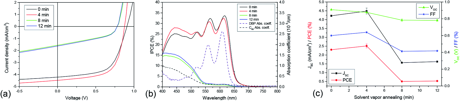 | ||
| Fig. 5 (a) J–V-characteristics, (b) IPCE curves with absorption spectra of DBP and C60 and (c) solar cell parameters vs. annealing time. The architecture of the solar cells is ITO(140 nm)/HIL1.3(45 nm)/DBP(30 nm)/C60(45 nm)/BCP(5 nm)/Al(100 nm). The times listed in (a) and (b) represent the time of SVA treatment, which is always done after evaporation of the donor DBP. | ||
Based on these results, the positive effects anticipated for SVA – the increase of ηED and ηCC – do indeed occur, however the duration of SVA must be precisely controlled in order to avoid significant aggregation of molecules within the film which deleteriously affects absorption and charge transport. A possible strategy to circumvent this problem would be to increase the DBP-layer thickness, as the enhanced crystallinity should allow a thicker film without negatively impacting RS or FF.21
III Solvent vapor annealing on crystalline donor DIP
In addition to DBP, we also tested the effect of solvent vapor annealing on DIP, which is known to grow crystalline in Stranski–Krastanov mode on various substrates.43,44 This means that a possible roughening effect caused by SVA is expected to be more pronounced on rather thin DIP layers, which are smoother than thicker ones due to its growth mechanism. Similar to DBP, XRR measurements do not reveal any change in the out-of-plane crystallinity due to SVA on 50 nm thick DIP layers. For the pristine as well as the SVA-treated sample, both the σ(001) and the σ(002)-peak appear at qz = 0.38 Å−1 and qz = 0.75 Å−1 respectively. Moreover, neither broadening of these peaks, which indicates a change in the vertical extent of the crystalline domains, nor the presence of additional peaks were detected. However, a distinct change of topography is visible by comparing the AFM images recorded on a 15 nm thick DIP layer which is either untreated or treated by SVA for four, eight, and twelve minutes, respectively (Fig. 6). The smooth surface of the pristine layer roughens continuously with increasing SVA time. The RMS roughness rises from 1.99 nm (0 min) to 2.14 nm (4 min) and 3.75 nm (8 min) up to 9.18 nm (12 min). Island-like structures appear on the surface with increasing diameters up to approximately 250 nm for the 12 minute sample. Thus, the increased surface roughness will provide increased D/A interface area upon evaporation of the acceptor. At the same time, AFM images indicate that the long-range order within the DIP donor increases and this should also lead to a similar increase of structural order in the subsequently evaporated C60 acceptor layer.45 In contrast to the DBP molecules, the DIP molecules do not aggregate strongly in the process of SVA resulting in a layer which is still continuous. As a result, a drastic decrease in absorption as was observed for the SVA treated DBP layer does not occur. In fact, absorption measurements even show a growing absorption coefficient, however it is just a minor effect. As this effect appears over the whole measured spectral range, it is assumed to be a measurement artifact due to increased scattering caused by the enhanced surface roughness. NEXAFS measurements were performed to clarify the origin of this behavior. Comparing pristine and annealed DIP layers, NEXAFS measurements show no change in angular dependence, meaning that there is also no change in molecular orientation and thus absorption strength. The corresponding data is shown in the ESI,† moreover, results of NEXAFS measurements on pristine DIP can also be found elsewhere.46,47 On the other hand, this confirms our interpretation that more scattering occurs at the DIP surface leading to an extended light path. In turn, this leads to more excitons generated within the organic.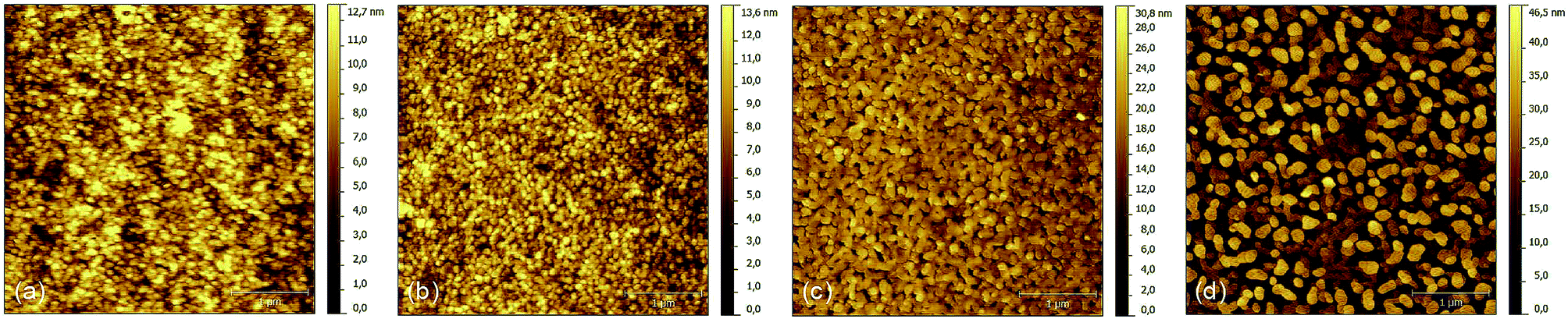 | ||
| Fig. 6 AFM images of a 15 nm DIP layer treated by SVA for (a) 0 minutes, (b) 4 minutes, (c) 8 minutes and (d) 12 minutes. | ||
As a result, the corresponding solar cells show a continuous increase in JSC. Based on the AFM images, absorption, and NEXAFS measurements, it can be assumed that both the enlarged interface as well as the extended light path due to enhanced scattering are responsible for this gain. Moreover, the FF increases by almost 10% while VOC remains unaffected. The gain in FF comes along with a decrease in RS, which drops continuously with increasing SVA time (Fig. 7(d)). As a consequence, the efficiency of DIP-based solar cells is improved through SVA by 16.8% (Fig. 7(a) and (c)). These results are comparable with improvements achieved using glancing angle deposition (GLAD).48 By the use of GLAD the D/A interface is enlarged as well, in this case however, by establishing nanocolumns using shadowing effects during the evaporation process.49 However, SVA is the more viable method as it is very easy to handle and does not require any sophisticated equipment. Summing up, it can be shown that also already crystalline layers can be affected positively using SVA. Again the efficiencies ηED and ηCC are raised, apparent from the gain in JSC and FF respectively. Moreover, negative effects like a strong aggregation or an unfavorable reorientation of the molecules accompanied with a decreasing ηAbs, which were observed for amorphous DBP, do not occur. However, as DIP inherently yields poor absorption, even for the SVA-treated case, the PCE is low. In this study it was increased from 1.55% (no treatment) to 1.8% with 12 minutes SVA.
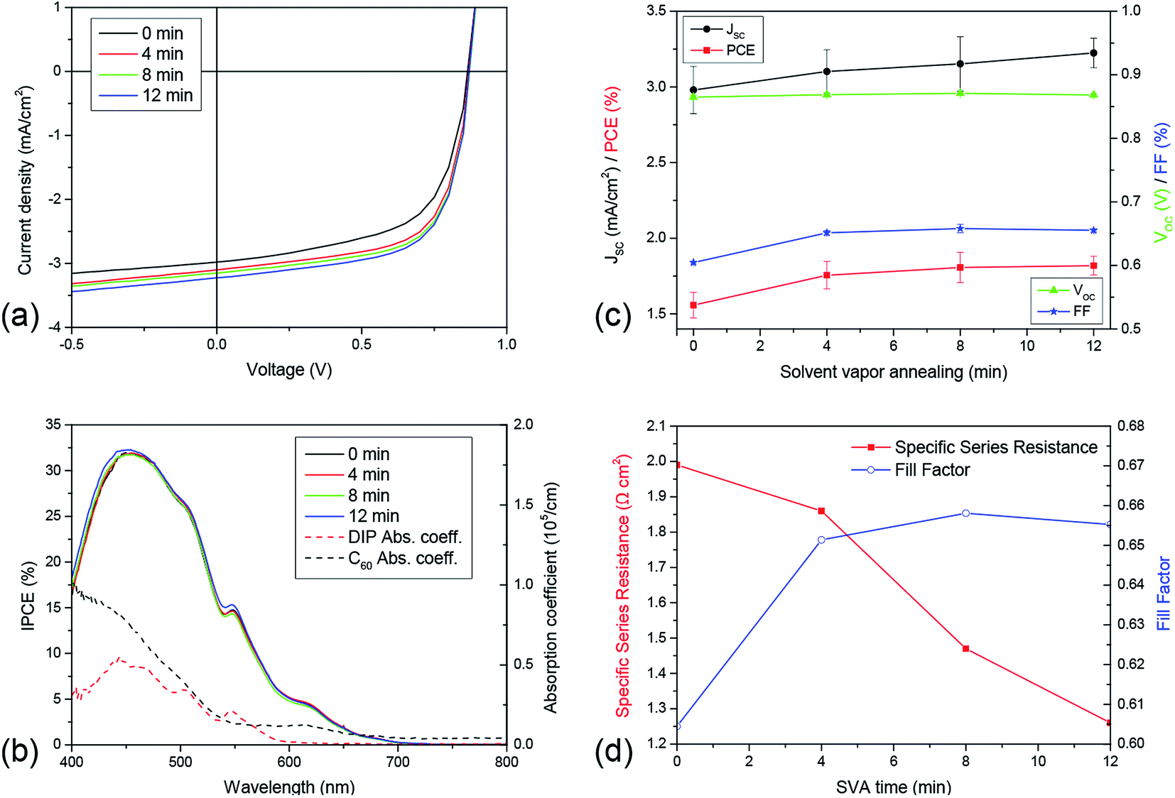 | ||
| Fig. 7 (a) J–V-characteristics, (b) IPCE curves with absorption spectra of DIP and C60, (c) solar cell parameters vs. annealing time and (d) development of RS and FF vs. SVA time. The architecture of the solar cells is ITO(140 nm)/HIL1.3(45 nm)/DIP(30 nm)/C70(45 nm)/BCP(5 nm)/Al(100 nm). The times listed in (a) and (b) represent the time of SVA treatment, which is always done after evaporation of the donor DIP. | ||
IV Solvent vapor annealing on exciton blocking layer DIP
In order to combine the positive effects observed for solvent vapor annealed DIP with the exciton blocking concept38,39 and using DBP and C70 as strongly absorbing donor and acceptor, respectively, planar photovoltaic cells are fabricated yielding overall efficiencies of more than 4%. The insertion of an exciton blocking layer at the anode interface provides an increase of η, mainly due to an increase in photocurrent, as excitons are prevented from being quenched at the HIL1.3/DBP interface. Moreover, we find that such solar cells can be further improved using SVA. However, it is not useful to perform the SVA after evaporation of DBP, because the strong aggregation of the molecules also occurs on a DIP substrate accompanied with the drop in absorption for longer SVA times. Absorption measurements even show that in this case the aggregation process of DBP already starts for shorter SVA times (see Fig. 3 in ESI†). As a consequence, the decrease of JSC and FF sets in for shorter SVA times, too.However, by treating only the exciton blocking layer, DIP, with solvent vapor, these parameters can be enhanced. The gain in JSC indicates that the SVA-induced increase in surface roughness of the DIP layer propagates to the DBP/C70 interface, where excitons dissociate and by that determine JSC. This is confirmed by AFM images of samples consisting of glass/45 nm HIL1.3/15 nm DIP/15 nm DBP. The annealing was performed on DIP for 4, 8 and 12 minutes. The RMS roughness of the surface of the subsequently evaporated DBP layer increases from 0.69 nm to 1.44 nm and 3.14 nm up to 4.24 nm. This means that the evaporation of the DBP layer smoothens the roughened DIP layer, however as desired, the D/A interface is enlarged compared to a pristine DBP film. Moreover, scattering that occurs at the rough DIP surface should enhance the path of the light through the DBP layer and by that also the absorption. Whether the enhanced crystallinity of the DIP layer also leads to a higher order in the amorphous DBP layer cannot be clearly confirmed. However, we suggest that this is the case, as again the FF of the corresponding photovoltaic cells increases while the values of their series resistance decline (Fig. 8(d)). This correlation is not linear, which shows that RS is just one factor contributing to FF.27 The expected gain in JSC appears (Fig. 8(a) and (b)) and the PCE can be increased by 20% from 3.4% to 4.1%. IPCE-curves (Fig. 8(c)) show that the gain in JSC caused by the insertion of the additional exciton blocking layer is mainly due to a greater contribution of excitons generated within the DBP layer. However, the SVA on DIP leads mainly to more contribution of the fullerene C70. A similar result was obtained for SVA on DBP (see Fig. 5(b)) where C60 was used as acceptor material. Thus, this trend is not influenced by changing the acceptor from C60 to C70.
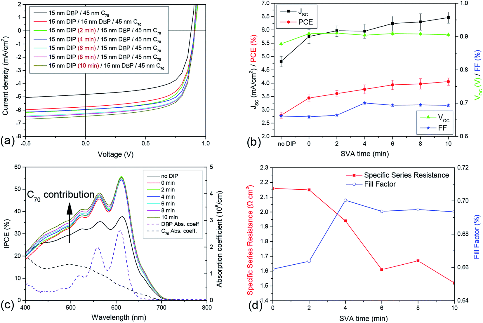 | ||
| Fig. 8 (a) J–V-characteristics, (b) solar cell parameters vs. annealing time, (c) IPCE curves with absorption spectra of DBP and C70 and (d) development of RS and FF vs. SVA time. The architecture of the solar cells is ITO(140 nm)/HIL1.3(45 nm)/DIP(15 nm)/DBP(15 nm)/C70(45 nm)/BCP(5 nm)/Al(100 nm). Moreover, data of a corresponding solar cell without the exciton blocking layer DIP are shown as reference. The times listed in (a) and (c) represent the time of SVA treatment, which is always done after evaporation of the blocking layer DIP. | ||
V Conclusion
In conclusion, solvent vapor annealing on perylene-based solar cells improves several processes contributing to the conversion of light to electrical power. In fact, SVA contributes to a majority of the sub-processes involved in various ways. For instance, the absorption efficiency ηAbs is influenced by an aggregation and/or by reorientation of the molecules. The reorganization process also leads to a higher structural order within the organic film. This enhanced crystallinity, resulting in a decreasing series resistance, has a positive impact on transport processes so that the efficiencies of exciton diffusion ηED and charge collection ηCC go up, resulting in a higher FF. Moreover, ηED is increased by a roughening of the D/A interface, as this enlargement enables more excitons to reach the interface before recombining within the bulk. In this way, a higher JSC can be achieved. However, we could show that the SVA-induced changes on organic solar cells are not necessarily positive and depend on some crucial correlations, which are different for each organic material. Thus, SVA has the potential to improve organic solar cells of various compositions, nevertheless for each material a suitable solvent, the best layer thickness, and a convenient SVA time has to be found.VI Experimental section
For SVA the substrate with the layer to be treated was laid face up in a small Petri dish. This Petri dish is then placed in a sealable vessel with 300 ml volume and 1 ml of chloroform is injected around the dish, so that there is no direct contact between solvent and sample. However, the solvent evaporates and the vapor can act on the organic material. The time is measured while the vessel is closed. The sample is then reinstalled into the evaporation chamber. Donor, acceptor, BCP and aluminum were all evaporated in UHV (<5 × 10⁻⁷ mbar) at 0.5 Å s−1. The PEDOT:PSS derivative HIL1.3 however, was spin-coated from aqueous dispersion and subsequently dried at 125 °C for 30 minutes. While HIL1.3 was obtained from Clevios (Germany), we purchased DBP from Lumtec (Taiwan), DIP from S. Hirschmann (Univ. Stuttgart, Germany) and BCP from Sigma-Aldrich (United States). The solar cell devices were characterized electrically by recording current–voltage (J–V) characteristics using a source measure unit (Keithley 236 SMU) under illumination with a solar simulator (Oriel 300 W with AM 1.5G filters) in a glovebox system with nitrogen atmosphere. The illumination intensity was approved by a calibrated silicon reference cell (RERA systems, PV Measurement Facility, Radboud University Nijmegen, area 1 × 1 cm2). Moreover, incident photon-to-current efficiency (IPCE) measurements were carried out using a monochromatized halogen lamp as light source and lock-in detection.In addition, a variety of measurements were carried out on pristine and SVA-treated organic (DIP, DBP) layers. Light microscopy was performed with a Zeiss Axioskop 40. Further, X-ray reflection (XRR) was done, both out-of-plane with a Seifert XRD 3003 PTS (CuKα1 radiation with λ = 1.541 Å) and also in-plane (grazing incidence X-ray diffraction, GIXD50) performed on the X04SA beamline at the Swiss Light Source, Paul Scherrer Institute, Villigen, Switzerland (12 keV photon energy).51 Atomic Force Microscopy (AFM52) data are acquired under ambient conditions with an Autoprobe CP-Research microscope from ThermoMicroscopes operated in tapping mode. To carry out absorption, transmittance and reflectance measurements were performed using a thin film analysis setup of omt GmbH. Moreover, angular resolved near edge X-ray absorption fine structure (NEXAFS) spectroscopy53 was measured at beamline D1011 (Max-lab, Lund, Sweden). Using polarized monochromatic X-rays around the C1s-edge, the total electron yield was determined by measuring the sample current.
Acknowledgements
This work was supported by the German Research Foundation (DFG) within the priority program SPP 1355 “Elementary Processes of Organic Solar Cells” and by the Bavarian State Ministry of Science, Research and the Arts within the collaborative research network “Solar Technologies go Hybrid”. S.G. and U.H. acknowledge the Bavarian Research Foundation (BFS), and C.L. thanks the Carl-Zeiss-Stiftung for Ph.D. scholarships. We thank Rickard Hansson and Leif K. E. Ericsson of the University of Karlstad, Sweden, and Paul Beyer, Humboldt University of Berlin, Germany, for experimental support and gratefully acknowledge Alexei Preobrajenski and Alexander Generalov for support at beamline D1011 at MaxIV laboratory as well as the MS-X04SA/Surface Diffraction beamline staff for their assistance during experiments at the Swiss Light Source.References
- K. Cnops, B. P. Rand, D. Cheyns, B. Verreet, M. A. Empl and P. Heremans, 8.4% efficient fullerene-free organic solar cells exploiting long-range exciton energy transfer, Nat. Commun., 2014, 5, 3406 CrossRef PubMed.
- X. Li, W. C. H. Choy, L. Huo, F. Xie, W. E. I. Sha, B. Ding, X. Guo, Y. Li, J. Hou, J. You and Y. Yang, Dual plasmonic nanostructures for high performance inverted organic solar cells, Adv. Mater., 2012, 24(22), 3046–3052 CrossRef CAS PubMed.
- X. Xiao, K. J. Bergemann, J. D. Zimmerman, K. Lee and S. R. Forrest, Small-molecule planar-mixed heterojunction photovoltaic cells with fullerene-based electron filtering buffers, Adv. Energy Mater., 2014, 4(7), 1301557 Search PubMed.
- Q. Zhang, B. Kan, F. Liu, G. Long, X. Wan, X. Chen, Y. Zuo, W. Ni, H. Zhang, M. Li, Z. Hu, F. Huang, Y. Cao, Z. Liang, M. Zhang, T. P. Russell and Y. Chen, Small-molecule solar cells with efficiency over 9%, Nat. Photonics, 2015, 9(1), 35–41 CrossRef CAS PubMed.
- K. Sun, Z. Xiao, S. Lu, W. Zajaczkowski, W. Pisula, E. Hanssen, J. M. White, R. M. Williamson, J. Subbiah, J. Ouyang, A. B. Holmes, W. W. H. Wong and D. J. Jones, A molecular nematic liquid crystalline material for high-performance organic photovoltaics, Nat. Commun., 2015, 6, 6013 CrossRef PubMed.
- B. Kan, M. Li, Q. Zhang, F. Liu, X. Wan, Y. Wang, W. Ni, G. Long, X. Yang, H. Feng, Y. Zuo, M. Zhang, F. Huang, Y. Cao, T. P. Russell and Y. Chen, A series of simple oligomer-like small molecules based on oligothiophenes for solution-processed solar cells with high efficiency, J. Am. Chem. Soc., 2015, 137(11), 3886–3893 CrossRef CAS PubMed.
- J. You, L. Dou, K. Yoshimura, T. Kato, K. Ohya, T. Moriarty, K. Emery, C.-C. Chen, J. Gao, G. Li and Y. Yang, A polymer tandem solar cell with 10.6% power conversion efficiency, Nat. Commun., 2013, 4, 1446 CrossRef PubMed.
- X. Che, X. Xiao, J. D. Zimmerman, D. Fan and S. R. Forrest, High-efficiency, vacuum-deposited, small-molecule organic tandem and triple-junction photovoltaic cells, Adv. Energy Mater., 2014, 4(18), 1400568 Search PubMed.
- J. Wagner, M. Gruber, A. Hinderhofer, A. Wilke, B. Bröker, J. Frisch, P. Amsalem, A. Vollmer, A. Opitz, N. Koch, F. Schreiber and W. Brütting, High fill factor and open circuit voltage in organic photovoltaic cells with diindenoperylene as donor material, Adv. Funct. Mater., 2010, 20(24), 4295–4303 CrossRef CAS PubMed.
- M. Gruber, M. Rawolle, J. Wagner, D. Magerl, U. Hörmann, J. Perlich, S. V. Roth, A. Opitz, F. Schreiber, P. Müller-Buschbaum and W. Brütting, Correlating Structure and Morphology to Device Performance of Molecular Organic Donor–Acceptor Photovoltaic Cells Based on Diindenoperylene (DIP) and C60, Adv. Energy Mater., 2013, 3(8), 10751083 Search PubMed.
- A. Opitz, J. Wagner, W. Brütting, I. Salzmann, N. Koch, J. Manara, J. Pflaum, A. Hinderhofer and F. Schreiber, Charge separation at molecular donor–acceptor interfaces: correlation between morphology and solar cell performance, IEEE J. Sel. Top. Quantum Electron., 2010, 16(6), 1707–1717 CrossRef CAS.
- A. K. Tripathi and J. Pflaum, Correlation between ambipolar transport and structural phase transition in diindenoperylene single crystals, Appl. Phys. Lett., 2006, 89(8), 082103 CrossRef PubMed.
- D. Kurrle and J. Pflaum, Exciton diffusion length in the organic semiconductor diindenoperylene, Appl. Phys. Lett., 2008, 92(13), 133306 CrossRef PubMed.
- A. C. Dürr, F. Schreiber, M. Münch, N. Karl, B. Krause, V. Kruppa and H. Dosch, High structural order in thin films of the organic semiconductor diindenoperylene, Appl. Phys. Lett., 2002, 81(12), 2276–2278 CrossRef PubMed.
- P. W. M. Blom, V. D. Mihailetchi, L. J. A. Koster and D. E. Markov, Device physics of polymer:fullerene bulk heterojunction solar cells, Adv. Mater., 2007, 19(12), 1551–1566 CrossRef CAS PubMed.
- P. Heremans, D. Cheyns and B. P. Rand, Strategies for increasing the efficiency of heterojunction organic solar cells: material selection and device architecture, Acc. Chem. Res., 2009, 42(11), 1740–1747 CrossRef CAS PubMed.
- M. Brinkmann, J. C. Wittmann, C. Chaumont and J. J. André, Effects of solvent on the morphology and crystalline structure of lithium phthalocyanine thin films and powders, Thin Solid Films, 1997, 292(1–2), 192–203 CrossRef CAS.
- F. Toffolo, M. Brinkmann, O. Greco, F. Biscarini, C. Taliani, H. L. Gomes, I. Aiello and M. Ghedini, Influence of the metal center on the morphology of coordination compounds thin films, Synth. Met., 1999, 101(1–3), 140–141 CrossRef CAS.
- D. J. Mascaro, M. E. Thompson, H. I. Smith and V. Bulović, Forming oriented organic crystals from amorphous thin films on patterned substrates via solvent-vapor annealing, Org. Electron., 2005, 6(5–6), 211–220 CrossRef CAS PubMed.
- J. D. Zimmerman, X. Xiao, C. K. Renshaw, S. Wang, V. V. Diev, M. E. Thompson and S. R. Forrest, Independent control of bulk and interfacial morphologies of small molecular weight organic heterojunction solar cells, Nano Lett., 2012, 12(8), 4366–4371 CrossRef CAS PubMed.
- B. Song, C. Rolin, J. D. Zimmerman and S. R. Forrest, Effect of mixed layer crystallinity on the performance of mixed heterojunction organic photovoltaic cells, Adv. Mater., 2014, 26(18), 2914–2918 CrossRef CAS PubMed.
- A. C. Dürr, F. Schreiber, K. A. Ritley, V. Kruppa, J. Krug, H. Dosch and B. Struth, Rapid roughening in thin film growth of an organic semiconductor (diindenoperylene), Phys. Rev. Lett., 2003, 90(1), 016104 CrossRef.
- D. Yokoyama, Z. Q. Wang, Y.-J. Pu, K. Kobayashi, J. Kido and Z. Hong, High-efficiency simple planar heterojunction organic thin-film photovoltaics with horizontally oriented amorphous donors, Sol. Energy Mater. Sol. Cells, 2012, 98, 472–475 CrossRef CAS PubMed.
- M. D. Perez, C. Borek, S. R. Forrest and M. E. Thompson, Molecular and morphological influences on the open circuit voltages of organic photovoltaic devices, J. Am. Chem. Soc., 2009, 131(26), 9281–9286 CrossRef CAS PubMed.
- U. Hörmann, J. Kraus, M. Gruber, C. Schuhmair, T. Linderl, S. Grob, S. Kapfinger, K. Klein, M. Stutzman, H. J. Krenner and W. Brütting, Quantification of energy losses in organic solar cells from temperature-dependent device characteristics, Phys. Rev. B: Condens. Matter Mater. Phys., 2013, 88(23), 235307 CrossRef.
- J. D. Servaites, S. Yeganeh, T. J. Marks and M. A. Ratner, Efficiency enhancement in organic photovoltaic cells: Consequences of optimizing series resistance, Adv. Funct. Mater., 2010, 20(1), 97–104 CrossRef CAS PubMed.
- B. Qi and J. Wang, Fill factor in organic solar cells, Phys. Chem. Chem. Phys., 2013, 15, 8972–8982 RSC.
- R. R. Lunt, J. B. Benziger and S. R. Forrest, Relationship between crystalline order and exciton diffusion length in molecular organic semiconductors, Adv. Mater., 2010, 22(11), 1233–1236 CrossRef CAS PubMed.
- S. Banerjee, A. Prasad Parhi, S. Sundar Kumar Iyer and S. Kumar, Method of determining the exciton diffusion length using optical interference effect in Schottky diode, Appl. Phys. Lett., 2009, 94(22), 223303 CrossRef PubMed.
- M. Hirade and C. Adachi, Small molecular organic photovoltaic cells with exciton blocking layer at anode interface for improved device performance, Appl. Phys. Lett., 2011, 99(15), 153302 CrossRef PubMed.
- J. J. M. Halls, C. A. Walsh, N. Greenham, E. A. Marseglia, R. Friend, S. C. Moratti and A. Holmes, Efficient photodiodes from interpenetrating polymer networks, Nature, 1995, 376, 498–500 CrossRef CAS PubMed.
- G. Yu, J. Gao, J. C. Hummelen, F. Wudl and A. J. Heeger, Polymer photovoltaic cells: enhanced efficiencies via a network of internal donor–acceptor heterojunctions, Science, 1995, 270(5243), 1789–1791 CAS.
- C. J. Brabec, G. Zerza, G. Cerullo, S. De Silvestri, S. Luzzati, J. C. Hummelen and S. Sariciftci, Tracing photoinduced electron transfer process in conjugated polymer/fullerene bulk heterojunctions in real time, Chem. Phys. Lett., 2001, 340(3–4), 232–236 CrossRef CAS.
- P. A. van Hal, R. A. J. Janssen, G. Lanzani, G. Cerullo, M. Zavelani-Rossi and S. De Silvestri, Full temporal resolution of the two-step photoinduced energy-electron transfer in a fullerene–oligothiophene–fullerene triad using sub-10 fs pump-probe spectroscopy, Chem. Phys. Lett., 2001, 345(1–2), 33–38 CrossRef CAS.
- G. Zerza, C. J. Brabec, G. Cerullo, S. De Silvestri and N. S. Sariciftci, Ultrafast charge transfer in conjugated polymer–fullerene composites, Synth. Met., 2001, 119(1–3), 637–638 CrossRef CAS.
- C. J. Brabec, N. S. Sariciftci and J. C. Hummelen, Plastic solar cells, Adv. Funct. Mater., 2001, 11(1), 15–26 CrossRef CAS.
- P. Peumans, A. Yakimov and S. R. Forrest, Small molecular weight organic thin-film photodetectors and solar cells, J. Appl. Phys., 2003, 93(7), 3693–3723 CrossRef CAS PubMed.
- Y. Zhou, T. Taima, T. Kuwabara and K. Takahashi, Efficient small-molecule photovoltaic cells using a crystalline diindenoperylene film as a nanostructured template, Adv. Mater., 2013, 25(42), 6069–6075 CrossRef CAS PubMed.
- S. Grob, M. Gruber, A. N. Bartynski, U. Hörmann, T. Linderl, M. E. Thompson and W. Brütting, Amorphous vs. crystalline exciton blocking layers at the anode interface in planar and planar-mixed heterojunction organic solar cells, Appl. Phys. Lett., 2014, 104(21), 213304 CrossRef PubMed.
- Y. Zhou, T. Taima, Y. Shibata, T. Miyadera, T. Yamanari and Y. Yoshida, Controlled growth of dibenzotetraphenylperiflanthene thin films by varying substrate temperature for photovoltaic applications, Sol. Energy Mater. Sol. Cells, 2011, 95(10), 2861–2866 CrossRef CAS PubMed.
- D. Bartesaghi and L. J. A. Koster, The effect of large compositional inhomogeneities on the performance of organic solar cells: a numerical study, Adv. Funct. Mater., 2015, 25(13), 2013–2023 CrossRef CAS PubMed.
- D. Gebeyehu, C. J. Brabec, F. Padinger, T. Fromherz, J. C. Hummelen, D. Badt, H. Schindler and N. S. Sariciftci, The interplay of efficiency and morphology in photovoltaic devices based on interpenetrating networks of conjugated polymers with fullerenes, Synth. Met., 2001, 118(1–3), 1–9 CrossRef CAS.
- S. Kowarik, A. Gerlach, S. Sellner, F. Schreiber, L. Cavalcanti and O. Konovalov, Real-time observation of structural and orientational transitions during growth of organic thin films, Phys. Rev. Lett., 2006, 96, 125504 CrossRef CAS.
- M. B. Casu, S.-A. Savu, B.-E. Schuster, I. Biswas, C. Raisch, H. Marchetto, Th. Schmidt and T. Chasse, Island shapes and aggregation steered by the geometry of the substrate lattice, Chem. Commun., 2012, 48(55), 6957–6959 RSC.
- A. Hinderhofer, A. Gerlach, K. Broch, T. Hosokai, K. Yonezawa, K. Kato, S. Kera, N. Ueno and F. Schreiber, Geometric and electronic structure of templated C60 on diindenoperylene thin films, J. Phys. Chem. C, 2013, 117(2), 1053–1058 CAS.
- M. B. Casu, I. Biswas, B.-E. Schuster, M. Nagel, P. Nagel, S. Schuppler and T. Chassé, Molecular orientation in diindenoperylene thin films deposited on polycrystalline gold, Appl. Phys. Lett., 2008, 93(2), 024103 CrossRef PubMed.
- U. Hörmann, C. Lorch, A. Hinderhofer, A. Gerlach, M. Gruber, J. Kraus, B. Sykora, S. Grob, T. Linderl, A. Wilke, A. Opitz, R. Hansson, A. S. Anselmo, Y. Ozawa, Y. Nakayama, H. Ishii, N. Koch, E. Moons, F. Schreiber and W. Brütting, V OC from a morphology point of view: the influence of molecular orientation on the open circuit voltage of organic planar heterojunction solar cells, J. Phys. Chem. C, 2014, 118(46), 26462–26470 Search PubMed.
- S. Yu, A. Opitz, S. Grob, R. Resel, M. Oehzelt, W. Brütting, I. Salzmann and N. Koch, Performance enhancement of diindenoperylene-based organic photovoltaic cells by nanocolumn-arrays, Org. Electron., 2014, 15(10), 2210–2217 CrossRef CAS PubMed.
- K. Robbie and M. J. Brett, Sculptured thin films and glancing angle deposition: growth mechanics and applications, J. Vac. Sci. Technol., A, 1997, 15(3), 1460–1465 CAS.
- W. C. Marra, P. Eisenberger and A. Y. Cho, X-ray total-external-reflection-Bragg diffraction: a structural study of the GaAs–Al interface, J. Appl. Phys., 1979, 50(11), 6927–6933 CrossRef CAS PubMed.
- P. R. Willmott, D. Meister, S. J. Leake, M. Lange, A. Bergamaschi, M. Böge, M. Calvi, C. Cancellieri, N. Casati, A. Cervellino, Q. Chen, C. David, U. Flechsig, F. Gozzo, B. Henrich, S. Jäggi-Spielmann, B. Jakob, I. Kalichava, P. Karvinen, J. Krempasky, A. Lüdeke, R. Lüscher, S. Maag, C. Quitmann, M. L. Reinle-Schmitt, T. Schmidt, B. Schmitt, A. Streun, I. Vartiainen, M. Vitins, X. Wang and R. Wullschleger, The Materials Science Beamline Upgrade at the Swiss Light Source, J. Synchrotron Radiat., 2013, 20(5), 667–682 CrossRef CAS PubMed.
- G. Binnig, C. F. Quate and Ch. Gerber, Atomic force microscope, Phys. Rev. Lett., 1986, 56, 930–933 CrossRef.
- J. Stöhr and D. A. Outka, Determination of molecular orientations on surfaces from the angular dependence of near-edge X-ray-absorption fine-structure spectra, Phys. Rev. B: Condens. Matter Mater. Phys., 1987, 36(15), 7891–7905 CrossRef.
Footnote |
| † Electronic supplementary information (ESI) available. See DOI: 10.1039/c5ta02806j |
| This journal is © The Royal Society of Chemistry 2015 |