
 Open Access Article
 This Open Access Article is licensed under a
 Creative Commons Attribution 3.0 Unported Licence
CH3NH3PbI3 perovskite single crystals: surface photophysics and their interaction with the environment†
G.
Grancini‡
 *a,
V.
D'Innocenzo
ab,
E. R.
Dohner
c,
N.
Martino
ab,
A. R.
Srimath Kandada
a,
E.
Mosconi
d,
F.
De Angelis
d,
H. I.
Karunadasa
c,
E. T.
Hoke
e and
A.
Petrozza
*a
*a,
V.
D'Innocenzo
ab,
E. R.
Dohner
c,
N.
Martino
ab,
A. R.
Srimath Kandada
a,
E.
Mosconi
d,
F.
De Angelis
d,
H. I.
Karunadasa
c,
E. T.
Hoke
e and
A.
Petrozza
*a
aCenter for Nano Science and Technology@Polimi, Istituto Italiano di Tecnologia, via Giovanni Pascoli 70/3, 20133, Milan, Italy. E-mail: giulia.grancini@epfl.ch; annamaria.petrozza@iit.it
bDipartimento di Fisica, Politecnico di Milano, Piazza L. da Vinci, 32, 20133 Milano, Italy
cDepartment of Chemistry, Stanford University, 337 Campus Drive, Stanford, California 94305, USA
dComputational Laboratory for Hybrid/Organic Photovoltaics (CLHYO), CNR-ISTM, Via Elce di Sotto 8, I-06123, Perugia, Italy
eDepartment of Materials Science and Engineering, Stanford University, 476 Lomita Mall, Stanford, California 94305, USA
First published on 17th September 2015
Abstract
Here we identify structural inhomogeneity on a micrometer scale across the surface of a CH3NH3PbI3 perovskite single crystal. At the crystal edge a local distortion of the crystal lattice is responsible for a widening of the optical bandgap and faster photo-carrier recombination. These effects are inherently present at the edge of the crystal, and further enhanced upon water intercalation, as a preliminary step in the hydration of the perovskite material.
Introduction
Hybrid perovskite based solar cells have already exceeded a certified power conversion efficiency of 20.1%.1,2 However, a clear understanding of the relationship between the optoelectronic properties of these materials and their morphology is lacking due to the large degree of structural variability within samples. Hybrid perovskites are usually deposited as polycrystalline thin-films with variable mesoscale morphology.3–5 Depending on the growth conditions, the obtained grain size typically ranges from tens to thousands of nm.3–5 To overcome this issue, perovskite single crystals are the ideal sample for understanding the inherent properties of the material, providing insight into their full potential once embodied in optoelectronic devices. However, several recent studies have reported conflicting optical properties for MAPbI3 (MA = CH3NH3+) single crystals.6–9 Here we provide a unifying picture, by highlighting the variation of the structural and optical properties across the crystal surface at a micrometer scale and by elucidating its interaction with the environment. Indeed, the optical properties we reveal at the crystal edges more closely resemble those of polycrystalline MAPbI3 thin films used in optoelectronic devices.10,11 These local probes of the structure and photophysical dynamics of the single crystal edge sites provide a systematic method for studying and optimizing the active interfaces, which are of high technological impact in polycrystalline perovskite films.Results and discussion
Fig. 1a–c shows the SEM image of the single crystal and higher resolution images of the region investigated. Specifically, we probe points at the centre of the crystal face (point A) or at the crystal edge (point B). The local photoluminescence spectra and dynamics have been measured with a spatial resolution of ∼1 μm (micro-PL hereafter, see the Experimental section for details) with the aim to probe the optical properties of the single crystal surface at a local scale. Example PL spectra and decay dynamics from the centre of the crystal face and the edge (taken at points A and B, respectively) are presented in Fig. 1d and e. The PL spectrum blue-shifts and the PL decay accelerates when moving from the centre to the crystal edge. In particular, the higher-energy PL from the crystal edge (Fig. 1c, point B) consists mainly of a fast component (∼40 ns, see Fig. 1e), along with a minor contribution from a long-lived tail (∼600 ns). On the contrary, for the lower-energy PL from the crystal centre (Fig. 1c and e, point A) the long-lived component dominates over the fast decay. Though the actual shift cannot be accurately quantified due to re-absorption effects that cannot be fully disregarded, together, these observations suggest that the spatial variation of the PL spectra arises from energetic inhomogeneity across the crystal. Such a conclusion can be further corroborated by looking at the spatial variation of the transient reflectance (TR) signal across the crystal face, which probes the semiconductor band edge (by monitoring the band edge photobleaching upon carrier cooling – see Fig. S1 in the ESI† with relative discussion).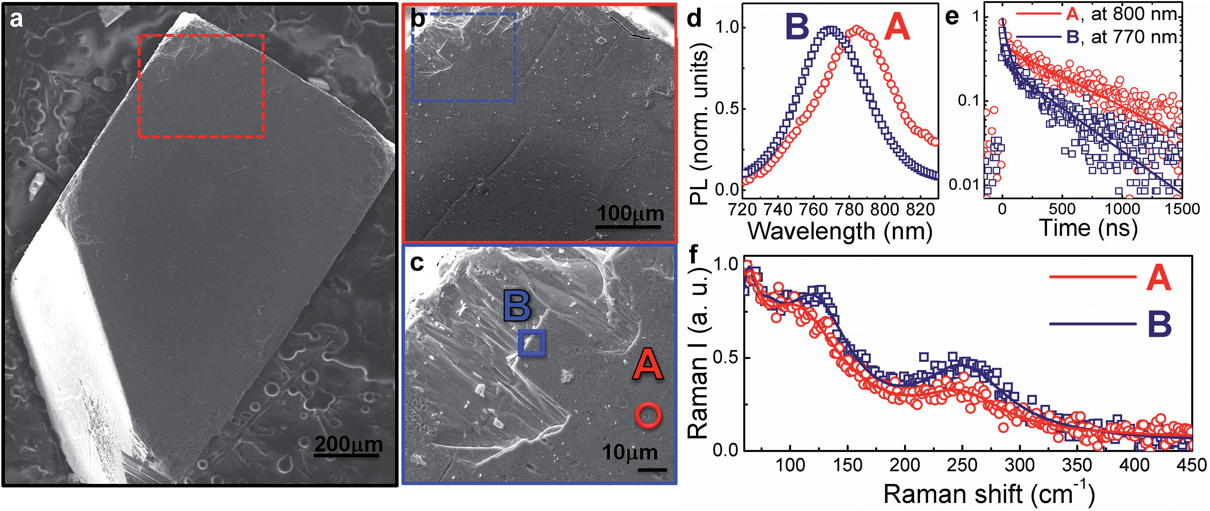 | ||
Fig. 1 (a) Top view SEM image of a mm-sized MAPbI3 single crystal (see Fig. S2† for XRD data); (b) enlarged view of the SEM in the top-left area of (a); (c) higher-resolution image of the SEM in the top-left area of (b) where spot A (towards the centre of the crystal face) and B (at the edge of the crystal face) have been measured, respectively; (d) PL spectra on spot A and B upon excitation at 690 nm (fluence ∼ 10 μJ cm−2) under a N2 atmosphere; (e) PL time decays at 770 nm (peak of point B PL spectrum) and 800 nm (peak of point A PL spectrum), solid lines represent the fits (y = 0.5![[thin space (1/6-em)]](https://www.rsc.org/images/entities/char_2009.gif) exp(−t/τ1) + 0.2exp(−t/τ2), τ1 = 630 ns, τ2 = 40 ns fits the decay at 800 nm; y = 0.2exp(−t/τ1) + 0.44exp(−t/τ2), τ1 = 500 ns, τ2 = 38 ns fits the decay at 770 nm). (f) Raman spectra from point B (blue squares) and point A (red dots) along with fitting results (solid lines). The measurement has been done under a N2 atmosphere. exp(−t/τ1) + 0.2exp(−t/τ2), τ1 = 630 ns, τ2 = 40 ns fits the decay at 800 nm; y = 0.2exp(−t/τ1) + 0.44exp(−t/τ2), τ1 = 500 ns, τ2 = 38 ns fits the decay at 770 nm). (f) Raman spectra from point B (blue squares) and point A (red dots) along with fitting results (solid lines). The measurement has been done under a N2 atmosphere. | ||
Considering that the excitation wavelength of 690 nm has an absorption depth of approximately 250 nm, surface effects (e.g., dangling bonds, under-coordinated atoms) will dominate the micro-PL measurement, certainly significant when probing the surface edges. We suggest that these edge surface effects are responsible for the blue-shifted, faster decaying component of the PL. In polycrystalline perovskite thin films it has been demonstrated11,12 that deformation of the inorganic cage through interactions with the organic cations can compress the lattice, resulting in an increased bandgap.11–15 Specific vibrational modes have been assigned as evidence for these lattice structural distortions.11,16,17
To better understand the origin of the spatially inhomogeneous PL, we measured the micro-Raman spectra at a ∼1 μm scale resolution on exactly the same points at which the micro-PL spectra were measured (Fig. 1f; see the Experimental section for details on the set-up). Excitation at the centre (point A) and the edge (point B) of the crystal face leads to different spectra, suggesting a restructuring of the crystal surface at the edges. The former shows a peak at 109 cm−1, assigned to the Pb–I stretching mode17 and a broad band at 250 cm−1, previously assigned to the torsional mode of the MA cation.11,17 When moving to the edge, we observe that the frequency of the Pb–I stretching mode is blue-shifted (towards 120 cm−1) and the peak gains intensity, while the band at 250 cm−1 slightly shifts and gets more intense. A similar trend has been previously observed for MAPbI3 nanocrystals grown within a mesoporous oxide scaffold, which were reported to be more distorted with respect to micrometer-size MAPbI3 crystallites deposited on a flat glass substrate.11 This result suggests that lattice strain at the crystal edges can be responsible for the blue-shifted PL. The above observations indicate that the edges of the MAPbI3 single crystal differ optically, energetically and structurally from the centre of the crystal face. This is not surprising, considering that defects and lattice reconstructions are common at crystal edges. Note also that the micro-PL spectra we measure at the crystal edges, rather than the crystal centre PL, more closely resemble the usual PL spectra observed for MAPbI3 polycrystalline thin films.10,11,19 Thus, we believe that the distorted crystal surface provides a model for the properties of polycrystalline thin films with small grains where surface effects at high defect densities, grain boundaries and active interfaces dominate and dramatically impact the device operation.18
Because the surface is exposed to the surrounding atmosphere, we investigated how the optical properties of the single crystal surface are sensitive to environmental interaction, in particular to the presence of moisture. The interaction between MAPbI3 and water is of particular concern as moisture has been shown to dramatically impact not only the perovskite film growth and crystallization dynamics20–25 but also accelerate material degradation.25–28Fig. 2 shows the macro-PL spectra measured on the whole crystal surface (a) under vacuum, (b) under low humidity (dry air with water content <10 ppm mol−1) and (c) under high humidity (ambient conditions, ∼50% relative humidity) (see Fig. S3† for a cartoon of the excitation–collection geometry).
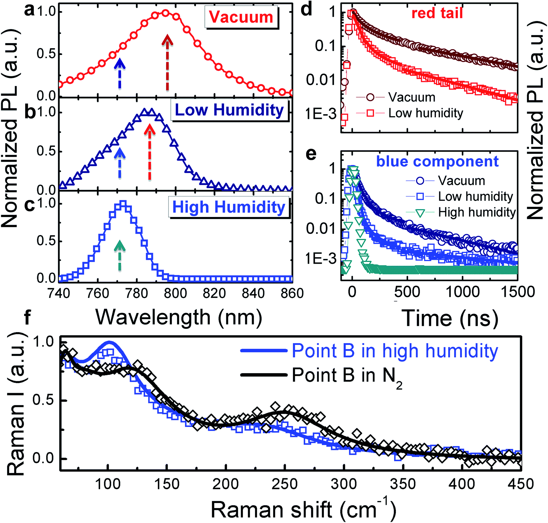 | ||
| Fig. 2 Normalized PL spectra (a–c) and dynamics (d and e, respectively) at the wavelengths indicated by the arrows in (a–c), collected under vacuum (a), under a low humidity atmosphere (b) and under high humidity (c); fluence ∼ 10 μJ cm−2. The solid lines in (2d and 2e) represent exponential fits: (y = 0.9exp(−t/τ1) + 0.1exp(−t/τ2)), τ1 = 35 ns τ2 = 240 ns fits the decay in vacuum; y = 0.95exp(−t/τ1) + 0.05exp(−t/τ2), τ1 = 26 ns, τ2 = 200 ns fits the decay under low humidity and y = exp(−t/τ), τ = 22 ns fits the decay under high humidity. (f) Comparison of the Raman spectra at point B, under dry N2versus under a high humidity environment. | ||
Here we are probing the signal from the whole crystal surface, including the edges. As shown, when under vacuum (Fig. 2a), the PL spectrum appears broad and asymmetric. Upon increasing exposure to humidity, the blue component becomes dominant (Fig. 2b and c) resulting in a sharp spectrum (FWHM ∼ 22 nm) peaking at 770 nm and the PL decay dynamics are shortened (Fig. 2d and e) showing a complete quenching of the longer-wavelength emission under ambient humidity. The PL spectra were taken within a few minutes of changing the test chamber atmosphere, indicating that the spectral changes are rapid. Such behaviour indicates that under ambient conditions, the reconstruction of the crystal surface induced by lattice distortion becomes more significant.
We hypothesize that the strained surface region grows and extends deeper into the crystal upon moisture exposure. Note that this phenomenon is partially reversible as shown by the recovery of the PL decay dynamics after storing the sample back under vacuum (Fig. S4†). To validate our hypothesis that exposure to the environment leads to a local distortion at the crystal surface we measured the micro-Raman spectra at the edge of the crystal in the presence of ambient humidity (Fig. 2f). In particular, the peak at 109 cm−1 shifts to lower energy and increases in intensity giving evidence for local distortion.11,17 Concomitantly, the MA cation mode at 250 cm-1 red shifts as well. Overall, this behaviour can be the result of water molecule interactions through hydrogen bonding with the organic cations and the halide ions. This is particularly relevant at the crystal edge. The centre of the crystal face, indeed, is less affected by interaction with humidity (see Fig. S5 in the ESI†).
We remark here that the widening of the band gap observed upon moisture exposure along with structural distortion happening at the crystal edges are distinct from the optical and structural features related to perovskite conversion into its hydrated phases.21,23,26 Hydrated forms of MAPbI3, such as the (CH3NH3)4PbI6·2H2O compound consisting of isolated PbI64− octahedra,21,23,26,29 are indeed pale yellow in colour, and exhibit a bandgap of over 3 eV and a zero-dimensional structure.21,23,26 We therefore believe that what we observe is likely an initial step of structural reorganization towards the conversion to a hydrated phase.
As evidenced by ab initio molecular dynamics simulations,30 water molecules can permeate across the perovskite structure to form a partly hydrated phase. Based on this preliminary observation, we further computationally simulated the possible phases obtained from stepwise perovskite hydration. To investigate how water and oxygen molecules can interact with the hybrid perovskite we calculated the formation energies for 4MAPbI3·nH2O and 4MAPbI3·O2, (Fig. 3a and b, respectively), by scalar-relativistic Perdew–Burke–Ernzerhof (PBE) calculations employing van der Waals corrections. Starting from a tetragonal unit cell, consisting of four MAPbI3 units, we sequentially add either one oxygen or up to four water molecules. The calculated relaxed atomic positions for 4MAPbI3·H2O and 4MAPbI3·O2 are shown in Fig. 3. Both structures exhibit an increase in cell volume of ∼11–12 Å3 with respect to MAPbI3. While the incorporation of one water molecule preserves the original tetragonal cell, with a ≈ b < c cell parameters, O2 interaction with MAPbI3 produces a sizable elongation/contraction of the a/b cell parameters (a = 8.61, b = 8.81, c = 12.82), respectively. Interestingly, as shown in Table S1 in the ESI,† the formation energy of 4MAPbI3·1H2O is negative, (−0.45 eV) indicating spontaneous water incorporation into the perovskite lattice. On the other hand, the incorporation of molecular oxygen is unfavourable, with a positive ΔEform of 0.17 eV.
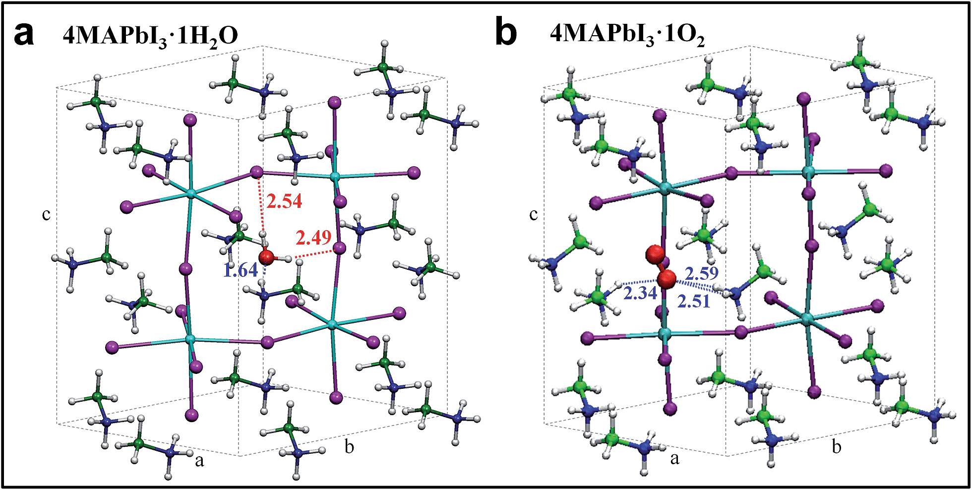 | ||
| Fig. 3 Optimized geometry structures for 4MAPbI3·1H2O (a) and 4MAPbI3·1O2 (b). Pb = light blue, I = violet, green = carbon, blue = nitrogen, red = oxygen, white = hydrogen. | ||
The driving force for water incorporation into the perovskite lattice is primarily the formation of hydrogen bonds between the water molecules and lattice iodides, as well as the tight hydrogen bonding interaction between one of the MA cations and the water oxygen atom, as signalled by a ∼1.6 Å separation distance between oxygen and one hydrogen atom of the MA cation (Fig. 3a). Notably, O2 interacts only through weaker hydrogen bonds with two vicinal MA cations, reflecting its lower tendency to be intercalated into the perovskite lattice. Water as well as oxygen (although less likely) incorporation into MAPbI3 increases the band gap by 50 and 90 meV, respectively, estimated here at the scalar-relativistic level of theory used for geometry optimization (see Table S1† for further details). While this level of theory is only able to accurately calculate the absolute bandgap values of lead halide perovskites due to a fortuitous cancelation of spin–orbit coupling effects,12 the calculated variations in bandgap are still valid. Subsequent incorporation of water molecules into MAPbI3 was also investigated up to 4:4 stoichiometries (see Table S1 and Fig. S6†). The results show that incorporation of a second water molecule has an essentially additive effect on the perovskite properties, with a slight additional volume and bandgap increase as a result of lattice distortion. However, adding four water molecules destabilizes the perovskite lattice, resulting in a large band gap increase. This is consistent with reports of a large band gap hydrated MAPbI3 phase with a non-perovskite structure.21,23,26,29 These findings support our experimental observations: the crystal edge surface, with a certain degree of distortion with respect to the bulk structure, is prone to water intercalation, resulting in a widening of the bandgap.
Experimental
MAPbI3 single crystal synthesis
All reagents were purchased from commercial vendors and used as received. Solid PbI2 (0.20 g, 0.43 mmol) and methylammonium iodide (0.069 g, 0.43 mmol) were added to 3 mL of acetonitrile. Hydroiodic acid (200 μL, 57 wt%, stabilized with 1.5% hypophosphorous acid) was added to the acetonitrile mixture, which was then sonicated for 5 minutes to ensure complete dissolution of the precursors. Dark, highly reflective block crystals were obtained by allowing diffusion of diethyl ether into this solution over a period of 2 days. The crystals were washed three times with diethyl ether and then dried under reduced pressure. Single crystals were stored under nitrogen and then cleaved along the (110) plane before optical measurements.Scanning electron microscopy (SEM)
The sample was placed on conductive carbon tape. SEM observation was carried out using a high vacuum tungsten filament commercial JEOL 6010-LV scanning electron microscope operating at 20 kV.Macro-photoluminescence
Time-resolved fluorescence measurements used for registering the spectra and dynamics in Fig. 2 were performed using a femtosecond laser source and a streak camera detection system (Hamamatsu C5680). For details on the experimental set-up see ref. 3 and 19. The measurements were generally carried out under vacuum and the environmental conditions are explicitly stated in the manuscript when other conditions were used.Micro-Raman and micro-PL spectroscopy
Our micro-Raman/PL system, used for the measurements presented in Fig. 1b–d and 2f, is based on an optical microscope (Renishaw microscope, see ref. 11 for further details on the experimental apparatus). Samples are excited with a 532 nm laser diode. For the Raman measurements the spectra were registered in the 60–500 cm−1 range. The final data were averaged over five hundreds acquisitions in order to improve the signal to noise ratio. The micro-PL was registered simultaneously on the same micrometer-large spot of the sample in back reflection geometry in the range between 700 and 850 nm. To prevent sample degradation or thermal effects, the laser power intensity is kept below 100 μW.Computational details
All calculations were carried out with the Quantum Espresso package along with the GGA-PBE functional. Electron–ion interactions were described by scalar relativistic ultrasoft pseudopotentials with electrons from O, N and C 2s, 2p; H 1s; I 5s, 5p; and Pb 6s, 6p, 5d shells explicitly included in the calculations. Variable cell geometry optimizations were carried out including a dispersion correction as in ref. 29. The formation energy of 4MAPbI3·nH2O has been evaluated as follows: ΔEform = E(4MAPbI3·nH2O) − E(4MAPbI3) − n × E(H2O), where E(4MAPbI3·nH2O) is the energy of the n-hydrated perovskite, E(4MAPbI3) is the energy of the anhydrous perovskite and E(H2O) is the energy of the isolated water molecule. The same approach has been used to evaluate the formation energy of 4MAPbI3·1O2.Conclusions
In conclusion, we demonstrate that the optical properties and band gap of MAPbI3 single crystals are spatially inhomogeneous, particularly at their edge surfaces. The edge surface exhibits a larger band gap and shorter carrier recombination dynamics with respect to the centre. We demonstrate that the origin of this variation is structural in nature, resulting from lattice strain which may be attributed to surface reconstruction at the crystal edges. The degree of strain at the crystal edges can be modulated by exposure to moisture and possibly oxygen to a lesser extent. The sensitivity of the perovskite single crystal optical properties to environmental conditions and the balance between surface and edge effects can explain the discrepancies in optical spectra reported so far in the literature.5–9 The crystal edge surface further acts as an open gate for the intercalation of water molecules, occurring spontaneously due to hydrogen bonding interactions with the perovskite lattice. This extends the depth of the surface region further into the bulk of the semiconductor, perhaps resulting in increased carrier trapping in optoelectronic devices. Regarding the moisture-induced degradation of perovskite optoelectronic devices, partial water intercalation into the perovskite structure is likely a necessary first step before structural conversion into a hydrate phase can occur. The observed blue-shift in the PL of perovskite crystals upon humidity exposure may provide an early warning signal before irreversible degradation occurs. Considering the tremendous interest in the application of such materials in optoelectronic devices, where the “interface is the device” (cit. Nobel laureate Herbert Kroemer) this work puts forward important information on the local properties of active interfaces and grain boundaries in polycrystalline perovskite films.Acknowledgements
The authors thank Dr F. Tassone, Dr James Ball and Dr Ilaria Bargigia for valuable discussion and Giovanni de Vecchi and Marina Gandini for the SEM image. The research leading to these results has received funding from the European Union Seventh Framework Program [FP7/2007-2013] under grant agreement no. 604032 of the MESO project. E.T.H. and E.R.D. were supported through the Global Climate and Energy Project (GCEP). Single-crystal X-ray precession images were obtained at beamline 11.3.1 at the Advanced Light Source (ALS). The ALS is supported by the Director, Office of Science, Office of Basic Energy Sciences, of the U.S. Department of Energy under contract no. DE-AC02-05CH11231.Notes and references
- H. Zhou, Q. Chen, G. Li, S. Luo, T.-b. Song, H.-s. Duan, Z. Hong, J. You, Y. Liu and Y. Yang, Science, 2014, 345, 542 CrossRef CAS PubMed.
- M. Grätzel, Nat. Mater., 2014, 13, 838 CrossRef PubMed.
- M. de Bastiani, V. D'Innocenzo, S. D. Stranks, H. J. Snaith and A. Petrozza, APL Mater., 2014, 2, 081509 CrossRef PubMed.
- J.-H. Im, I.-H. Jang, N. Pellet, M. Grätzel and N.-G. Park, Nat. Nanotechnol., 2014, 9, 927 CrossRef CAS PubMed.
- H. Yu, F. Wang, F. Xie, W. Li, J. Chen and N. Zhao, Adv. Funct. Mater., 2014, 24, 7102 CAS.
- D. Shi, V. Adinolfi, R. Comin, M. Yuan, E. Alarousu, A. Buin, Y. Chen, S. Hoogland, A. Rothenberger, K. Katsiev, Y. Losovyj, X. Zhang, P. A. Dowben, O. F. Mohammed, E. H. Sargent and O. M. Bakr, Science, 2015, 347, 519 CrossRef CAS PubMed.
- Q. Dong, Y. Fang, Y. Shao, P. Mulligan, J. Qiu, L. Cao and J. Huang, Science, 2015, 347, 967 CrossRef CAS PubMed.
- W. Nie, H. Tsai, R. Asadpour, J. C. Blancon, A. J. Neukirch, G. Gupta, J. J. Crochet, M. Chhowalla, S. Tretiak, M. A. Alam, H.-L. Wang and A. D. Mohite, Science, 2015, 347, 522 CrossRef CAS PubMed.
- H. H. Fang, R. Raissa, M. Abdu-Aguye, S. Adjokatse, G. R. Blake, J. Even and M. A. Loi, Adv. Funct. Mater., 2015, 25, 2378 CrossRef CAS PubMed.
- D. W. de Quilettes, S. M. Vorpahl, S. D. Stranks, H. Nagaoka, G. E. Eperon, M. E. Ziffer, H. J. Snaith and D. S. Ginger, Science (Washington, DC, U. S.), 2015, 348, 683 CrossRef CAS PubMed.
- G. Grancini, S. Marras, M. Prato, C. Giannini, C. Quarti, F. de Angelis, M. de Bastiani, G. E. Eperon, H. J. Snaith, L. Manna and A. Petrozza, J. Phys. Chem. Lett., 2014, 5, 3836 CrossRef CAS PubMed.
- E. Mosconi, A. Amat, M. K. Nazeeruddin, M. Grätzel and F. de Angelis, J. Phys. Chem. C, 2013, 117, 13902 CAS.
- J. J. Choi, X. Yang, Z. M. Norman, S. J. L. Billinge and J. S. Owen, Nano Lett., 2014, 14, 127 CrossRef CAS PubMed.
- M. R. Filip, G. E. Eperon, H. J. Snaith and F. Giustino, Nat. Commun., 2014, 5, 5757 CrossRef CAS PubMed.
- A. Amat, E. Mosconi, E. Ronca, C. Quarti, P. Umari, M. K. Nazeeruddin, M. Grätzel and F. de Angelis, Nano Lett., 2014, 14, 3608 CrossRef CAS PubMed.
- E. Mosconi, C. Quarti, T. Ivanovska, G. Ruani and F. de Angelis, Phys. Chem. Chem. Phys., 2014, 16, 16137 RSC.
- C. Quarti, G. Grancini, E. Mosconi, P. Bruno, J. M. Ball, M. M. Lee, H. J. Snaith, A. Petrozza and F. de Angelis, J. Phys. Chem. Lett., 2014, 5, 279 CrossRef CAS PubMed.
- E. T. Hoke, D. J. Slotcavage, E. R. Dohner, A. R. Bowring, H. I. Karunadasa and M. D. McGehee, Chem. Sci., 2015, 6, 613 RSC.
- V. D'Innocenzo, A. R. Srimath Kandada, M. de Bastiani, M. Gandini and A. Petrozza, J. Am. Chem. Soc., 2014, 136, 17730 CrossRef PubMed.
- C. Motta, F. El-Mellouhi, S. Kais, N. Tabet, F. Alharbi and S. Sanvito, Nat. Commun., 2015, 6, 7026 CrossRef CAS PubMed.
- A. Leguy, Y. Hu, M. Campoy-Quiles, M. I. Alonso, O. J. Weber, P. Azarhoosh, M. van Schilfgaarde, M. T. Weller, T. Bein, J. Nelson, P. Docampo and P. R. F. Barnes, Chem. Mater., 2015, 27, 3397 CrossRef CAS.
- J. You, Y. (M. ) Yang, Z. Hong, T.-b. Song, L. Meng, Y. Liu, C. Jiang, H. Zhou, W.-H. Chang, G. Li and Y. Yang, Appl. Phys. Lett., 2014, 105, 183902 CrossRef PubMed.
- J. A. Christians, P. A. Miranda Herrera and P. V. Kamat, J. Am. Chem. Soc., 2015, 137, 1530 CrossRef CAS PubMed.
- X. Dong, X. Fang, M. Lv, B. Lin, S. Zhang, J. Ding and N. Yuan, J. Mater. Chem. A, 2015, 3, 5360 CAS.
- K. K. Bass, R. E. McAnally, S. Zhou, P. I. Djurovich, M. E. Thompson and B. C. Melot, Chem. Commun., 2014, 50, 15819 RSC.
- J. Yang, B. D. Siempelkamp, D. Liu and T. L. Kelly, ACS Nano, 2015, 9, 1955 CrossRef CAS PubMed.
- S. Pathak, A. Sepe, A. Sadhanala, F. Deschler, A. Haghighirad, N. Sakai, K. C. Goedel, S. D. Stranks, N. Noel, M. Price, S. Hüttner, N. A. Hawkins, R. H. Friend, U. Steiner and H. J. Snaith, ACS Nano, 2015, 9, 2311 CrossRef CAS PubMed.
- N. Aristidou, I. Sanchez-Molina, T. Chotchuangchutchaval, M. Brown, L. Martinez, T. Rath and S. A. Haque, Angew. Chem., 2015, 127, 8326 CrossRef PubMed.
- B. R. Vincent, K. N. Robertson, T. S. Cameron and O. Knop, Can. J. Chem., 1987, 65, 1042 CrossRef CAS.
- E. Mosconi, J. M. Azpiroz and F. de Angelis, Chem. Mater., 2015, 27, 4885 CrossRef CAS.
Footnotes |
| † Electronic supplementary information (ESI) available. See DOI: 10.1039/c5sc02542g |
| ‡ Present address: EPFL Valais Wallis, Rue de l'Industrie 17, CH-1951 Sion, Switzerland. |
| This journal is © The Royal Society of Chemistry 2015 |