
 Open Access Article
 This Open Access Article is licensed under a
 Creative Commons Attribution 3.0 Unported Licence
Low ensemble disorder in quantum well tube nanowires†
Christopher L.
Davies
*a,
Patrick
Parkinson
 b,
Nian
Jiang
c,
Jessica L.
Boland
a,
Sonia
Conesa-Boj
a,
H. Hoe
Tan
c,
Chennupati
Jagadish
c,
Laura M.
Herz
a and
Michael B.
Johnston
*a
b,
Nian
Jiang
c,
Jessica L.
Boland
a,
Sonia
Conesa-Boj
a,
H. Hoe
Tan
c,
Chennupati
Jagadish
c,
Laura M.
Herz
a and
Michael B.
Johnston
*a
aDepartment of Physics, University of Oxford, Clarendon Laboratory, Parks Road, Oxford, OX1 3PU, UK. E-mail: michael.johnston@physics.ox.ac.uk
bSchool of Physics and Astronomy and the Photon Science Institute, University of Manchester, Manchester M13 9PL, UK
cDepartment of Electronic Materials Engineering, Research School of Physics and Engineering, The Australian National University, Canberra, ACT 0200, Australia
First published on 6th November 2015
Abstract
We have observed very low disorder in high quality quantum well tubes (QWT) in GaAs-Al0.4Ga0.6As core–multishell nanowires. Room-temperature photoluminescence spectra were measured from 150 single nanowires enabling a full statistical analysis of both intra- and inter-nanowire disorder. By modelling individual nanowire spectra, we assigned a quantum well tube thickness, a core disorder parameter and a QWT disorder parameter to each nanowire. A strong correlation was observed between disorder in the GaAs cores and disorder in the GaAs QWTs, which indicates that variations in core morphology effectively propagate to the shell layers. This highlights the importance of high quality core growth prior to shell deposition. Furthermore, variations in QWT thicknesses for different facet directions was found to be a likely cause of intra-wire disorder, highlighting the need for accurate shell growth.
1. Introduction
Semiconductor nanowires have received much attention over the past decade owing to their potential use in electronic and optoelectronic devices. Already many nanowire based devices have been demonstrated, including solar cells,1,2 terahertz detectors,3–5 field effect transistors,6,7 electrical detection of cancer markers8 and LED-based devices.9,10 Customisation of the band gap is essential for such nanowire applications. While adjusting the alloy fraction of ternary materials such as AlxGa1−xAs is traditionally used to tailor the band gap of semiconductors, tuning the nanowire band gaps across the full visible region has proved challenging.11 An alternative method for tailoring the band gap energy is to take advantage of quantum effects: by growing a thin layer of lower band gap material within the higher band gap shell layer, a “quantum well tube” (QWT), or “radial quantum well”, along the nanowire axis can be produced.Core–multishell nanowires have previously been fabricated in a range of material systems from nitride,12 phosphide,13 and arsenide14 based III–Vs, to silicon.15–17 Furthermore, they have already been implemented in a range of optoelectronic devices.18–22 Small changes in the width of the QWT shell layers result in large changes in the confinement energy with an associated significant impact on the emitted spectrum. Control of the size of the core and shell layers, as well as the intra-wire energetic disorder in each layer, is therefore crucial to the development of nanowire-based devices. In order to achieve good repeatability needed for large-scale device manufacturing, it is important to understand the underlying mechanisms causing inter-nanowire variations. For commercial applications, characterisation of nanowires at room temperature is highly desirable. Previous studies have been carried out at low temperature to characterise single QWTs,23–25 unfortunately room temperature measurements have, until now, remained challenging owing to quenching and broadening effects in the photoluminescence (PL) emission spectrum.
In this report, we have conducted PL measurements on 150 single GaAs/Al0.4Ga0.6As core–multishell nanowires to investigate the statistical distributions of the structural and optical properties that result from growing a thin GaAs shell layer (QWT) between two thicker Al0.4Ga0.6As shell layers. We observe that charge carriers in the QWT are confined in one dimension, resulting in a blue shift of the allowed transitions associated with PL emission (ΔE = 0.1–0.3 eV). A simple one-dimensional (1D) finite well model for the QWT was implemented to obtain an estimate of the well width. Furthermore, statistics have been collected on 150 nanowires from 3 different samples and used to examine the intra-sample and inter-sample variations in nanowire thicknesses and defects. We report low disorders for both the core and QWT and discuss correlations between them and their structure. Two-dimensional (2D) numerical simulations have also been performed to investigate the effect of introducing geometric distortions and disorder on the optical and electronic properties of nanowires.
2. Method
2.1. Growth method
Core–multishell GaAs/Al0.4Ga0.6As QWT nanowires have been grown by metalorganic chemical vapor deposition with various QWT widths in order to investigate energetic disorder. Trimethylgallium (TMGa), trimethylaluminium (TMAl), and arsine (AsH3) were used for the source of Ga, Al, and As, respectively. First, GaAs nanowires were grown on GaAs (111)B substrates by a two-temperature procedure26 using Au nanoparticles with a diameter of, 50 nm, 100 nm and 100 nm, as the catalysts of samples we will label, B50, B100 and C100, respectively. After the 50 nm (100 nm) core growth, the growth temperature was increased to 750 °C and then a 23 nm (46 nm) AlGaAs layer was deposited surrounding the core, followed by the GaAs QWT growth by switching off TMAl. The thicknesses of GaAs QWTs were controlled by the growth time, which was 30 and 15 seconds for the B and C samples respectively. This resulted in QWT thicknesses of approximately, 1.5 nm, 3 nm and 2 nm, for the three samples respectively. The GaAs QWT was then enclosed in another AlGaAs layer with thickness 16 nm (32 nm). As a result, a GaAs QWT sandwiched between two AlGaAs layers was obtained in the nanowire. Finally, a thin layer of GaAs was deposited as a capping layer to prevent the oxidation of Al in the AlGaAs shell. The aluminium concentration has been determined previously to be 0.40 ± 0.06 in the AlGaAs barriers.23 This was measured by aberration-corrected high-angle annular dark field scanning transmission electron microscopy images taken on nanowires grown by the same method. After growth, the nanowires were transferred from their growth wafers to quartz substrates by rubbing.2.2. Experimental method
Time-integrated PL measurements were performed at room temperature using a custom-built microscope. Two 50![[thin space (1/6-em)]](https://www.rsc.org/images/entities/char_2009.gif) :50 beam splitters were used in the system to observe, excite and collect PL from the nanowires. Incident light was focused onto the sample using a 40× infinity objective with a numerical aperture of 0.65 and the spot size measured to be 1.5 ± 0.1 μm. The Abbe diffraction limit of this setup was approximately 400 nm, small enough to observe single nanowires under back illumination due to efficient light scattering. Single nanowires were located by back illumination of the sample and observed through the same objective used to focus the laser. A Ti:sapphire laser combined with an optical parametric oscillator (OPO) was used to excite the sample with 100 fs pulses of 532 nm (2.33 eV) photons at a repetition rate of 80 MHz. The average power used was 3 μW (equivalent to 2.2 μJ cm−2 per pulse). Excitation power dependent measurements were taken to confirm emitted PL was in the linear regime. The PL was detected using a grating spectrometer and liquid nitrogen cooled charge coupled device (CCD) array. The system was corrected for spectral response. Reflections and scatter of the laser from the sample substrate were blocked using a 575 nm and 590 nm long pass filter. The PL was observed to be strongest at the ends of the nanowires as a result of waveguiding.30–32 The PL from the QWT was sensitive to the position of the incident light on the nanowire33 and measurements were taken at a position where the emissions from the core and QWT were approximately of the same order of intensity.
:50 beam splitters were used in the system to observe, excite and collect PL from the nanowires. Incident light was focused onto the sample using a 40× infinity objective with a numerical aperture of 0.65 and the spot size measured to be 1.5 ± 0.1 μm. The Abbe diffraction limit of this setup was approximately 400 nm, small enough to observe single nanowires under back illumination due to efficient light scattering. Single nanowires were located by back illumination of the sample and observed through the same objective used to focus the laser. A Ti:sapphire laser combined with an optical parametric oscillator (OPO) was used to excite the sample with 100 fs pulses of 532 nm (2.33 eV) photons at a repetition rate of 80 MHz. The average power used was 3 μW (equivalent to 2.2 μJ cm−2 per pulse). Excitation power dependent measurements were taken to confirm emitted PL was in the linear regime. The PL was detected using a grating spectrometer and liquid nitrogen cooled charge coupled device (CCD) array. The system was corrected for spectral response. Reflections and scatter of the laser from the sample substrate were blocked using a 575 nm and 590 nm long pass filter. The PL was observed to be strongest at the ends of the nanowires as a result of waveguiding.30–32 The PL from the QWT was sensitive to the position of the incident light on the nanowire33 and measurements were taken at a position where the emissions from the core and QWT were approximately of the same order of intensity.
3. Results and discussion
A schematic diagram of the band structure of one of the QWT nanowires is displayed in Fig. 1a, with the transition energies from the core and the quantum well tube indicated. A typical spectrum is shown in Fig. 1b, with the peak of the QWT shifted higher in energy owing to confinement. This confinement in nanowire heterostructures has been documented previously at low temperature23–25 with some studies of axial heterostructures reporting this effect at room temperatures.34 We demonstrate this effect at room temperature for radial heterostructures; and more importantly, using measurements taken on single nanowires.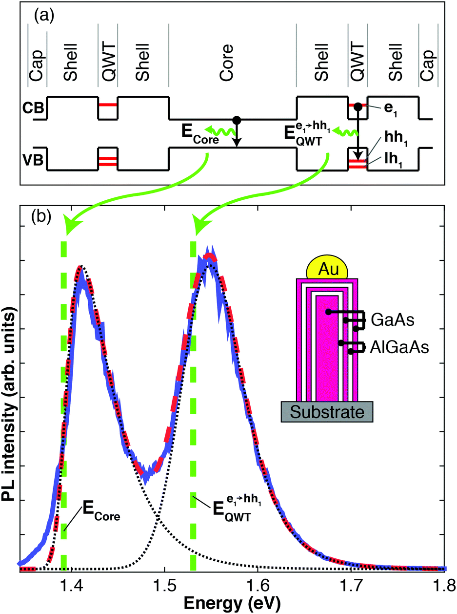 | ||
| Fig. 1 (a) Schematic of the band structure of a nanowire taken along a line perpendicular to and intersecting the nanowire axis. The black lines show the conduction band (CB) and the valence band (VB), with black arrows depicting the electronic transitions from the core and the QWT with emission energies ECore and EQWT respectively. The horizontal red lines show the ground state energies, which are shifted with respect to the bulk values owing to quantum confinement. The nanowire is composed of: a GaAs core; two Al0.4Ga0.6As shell barrier layers with a GaAs QWT in-between; and a GaAs capping layer. (b) A PL spectrum from a typical nanowire from sample B100 (shown on a linear scale). Experimental data is shown as a blue solid line, the model as a red dashed line, and the core and QWT components of the model as black dashed lines. The two green dashed lines show the energy gap of the core and the QWT. The inset shows a schematic of the nanowire showing the GaAs core, QWT and cap, and the Al0.4Ga0.6As shell barrier layers. | ||
3.1. Model
The carrier lifetime for GaAs/Al0.4Ga0.6As core–shell nanowires grown using the two-temperature technique26 has been previously measured to be of the order of nanoseconds.27 Following pulsed excitation, photo-injected electrons and holes rapidly establish a thermal distribution near the conduction and valence band edges.35 As excitonic effects are weak at room temperature in GaAs36,37 we assume the PL spectrum of each nanowire is dominated by band-to-band recombination in both the core and QWT. To a first approximation, the emission energy spectrum in a 3D semiconductor is proportional to a Fermi–Dirac distribution multiplied by the density of states. At room temperature, thermal energies are large enough that we can approximate this Fermi–Dirac distribution using the classical limit to a Boltzmann distribution, with an energy-offset equal to the band gap energy, multiplied by the joint density of states for the electrons and holes. This approximated distribution can then be used to model the expected emission peak from the core and the QWT respectively. The core has a three-dimensional (3D) density of states (DoS), as the width is large enough such that quantum confinement effects are insignificant.38 Thus, for the core with band gap, ECore, we simply fit a Maxwell–Boltzmann distribution, | (1) |
 | (2) |
 . The nanowires, however, do not have a perfect structure and so the spectral peaks are broadened by defects and disorder. In order to parameterise disorder, we introduce a Gaussian distribution:
 | (3) |
 ) of the PL spectrum in the absence of thermal broadening (i.e. in the limit T → 0). The intensity of each peak is therefore proportional to the convolution of G(E) and B(E). Thus, we model the intensity of measured PL, I(E), as a linear combination of the core and QWT intensities,
| I(E) ∝ GCore(E) ⊗ BCore(E) + GQWT(E) ⊗ BQWT(E). | (4) |
From this model, the following parameters could then be determined: the emission energy of the core (ECore) and QWT  ; the disorder parameter of the core (σCore) and QWT (σQWT); and the electron temperature (T). The electron temperature extracted from fits to the data (average: 360 ± 60 K) was significantly above the lattice temperature (290 K) as expected.41,42 Finally, a finite well model was used to extract the well width for the QWT. While excited charge carriers do relax to lower energy states, we have observed that a significant number of charge carriers have larger energies than the energetic disorder parameter. These carriers can occupy states in thinner sections of the QWT and therefore we are able to probe all parts of the QWT and not just the thicker sections. Further detail on the modelling is included in the ESI.†
3.2. Results
The PL spectrum of a typical single nanowire from sample B100 is shown in Fig. 1b. The spectrum is composed of two broad peaks; the peak at 1.42 eV is the emission from the GaAs core and the peak at 1.55 eV is attributed to a blue shift in the e1 → hh1 transition in the GaAs QWT layer owing to quantum confinement. The red dashed line in Fig. 1b is a fit of eqn (4) to the measured PL spectrum. The fit accurately reproduces both the core and QWT emission peaks, with only a minor discrepancy in the low energy tails (<1.4 eV). These low energy tails probably arise from defect level recombination, aluminium-induced red shifts,43 or residual strain,44 and have been reported previously for bulk samples.45The fitted values for the band gap energy and QWT transition energy are ECore = 1.39 eV and  = 1.53 eV respectively, and are indicated by the two green dashed lines in Fig. 1b. The fact that these values differ from the peak energies in the PL spectrum by ∼30 meV highlights the importance of properly modelling PL spectra from nanowires. In this case the value of the experimentally observed peaks are shifted from the true transition energies as a result of two factors: (i) asymmetric thermal broadening37,46 and (ii) the fact the PL emission from the QWT and core overlap spectrally. Both these effects are accounted for in eqn (4). For example by changing photo-excitation conditions the relative intensities of the two spectrally overlapping PL peaks change. Despite changes in the PL peak positions, our model reveals the same transition energies ECore and
  , irrespective of such changes in relative PL intensity.
Measurements of the well width were calculated using the finite well model and are presented in a histogram plot in Fig. 2. The average widths are 2.1, 4.0 and 2.0 nm, for samples B50, B100 and C100, respectively. The main source of error in the calculated quantum well widths is from the uncertainty in the fitting of the energy of the core and QWT emission peaks. The lattice spacing of the 220 atomic planes has previously been measured to be 0.2 nm.27 The standard deviation of the QWT width of each sample was measured to be 0.32, 0.14 and 0.10 nm. Thus, these results provide evidence of the inter-wire uniformity and consistency of the QWT layer growth, which is promising for scaling the production of nanowires.
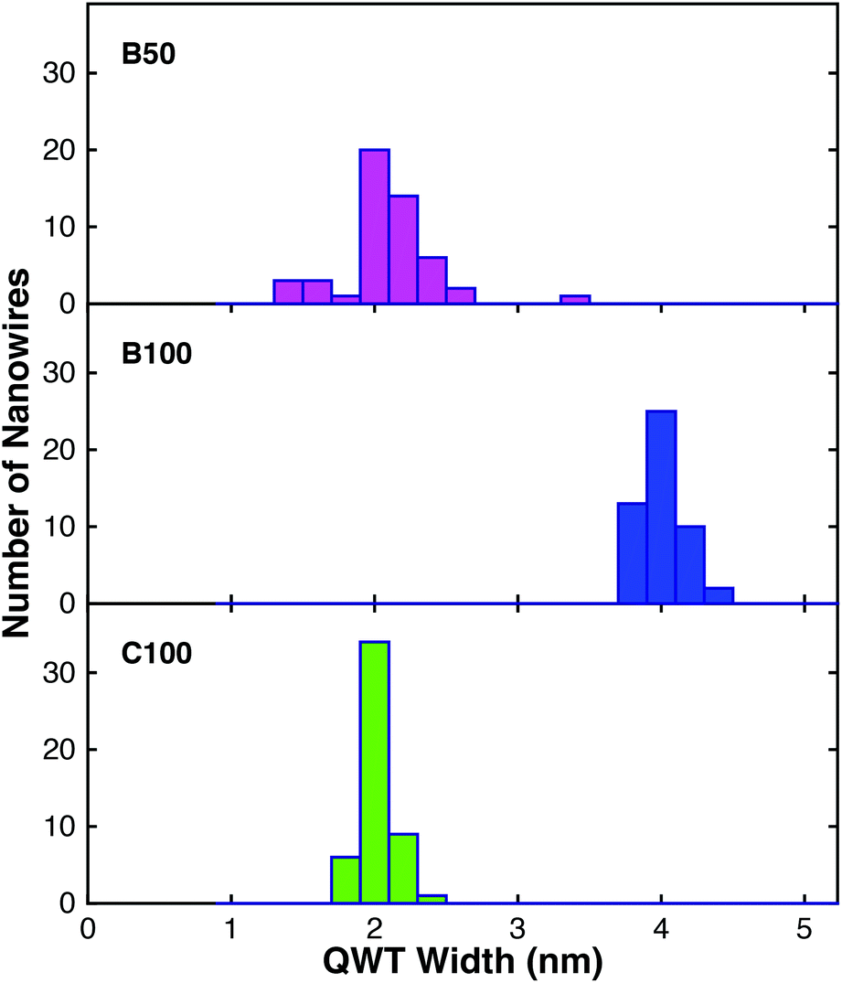 | ||
| Fig. 2 A histogram of all nanowires measured showing the occurrence of the QWT widths in each sample, as measured using the modelled PL spectra. The average widths are 2.1, 4.0 and 2.0 nm, for the B50, B100 and C100 samples, respectively. | ||
The disorder parameter we extract encompasses all possible energetic sources of disorders in our system. Here, we discuss these contributing factors. Our nanowires were determined to be twin free,27–29 so structural defects are considered to be negligible. The main factors contributing to the disorder are width fluctuations and variations in Al alloy fraction. Both of these factors affect the degree of confinement felt by charge carriers in the QWT and therefore the energy of emission on relaxation of these charge carriers. The width of the GaAs layer between the AlGaAs barrier layers defines the width of the well and the Al concentration defines the barrier height. The contribution of Al concentration fluctuations to the disorder has been calculated to be 68, 34 and 74 percent of the total value for the B50, B100 and C100 samples, respectively (as detailed in Fig. S7 of the ESI†).
Using the calculated well widths, a relationship between both the energy peak and QWT width with the disorder parameter was observed, as shown in Fig. 3a. The larger well widths are correlated with smaller disorder parameters. Notably, sample B100 has both a significantly larger well width than the other two samples as well as a much smaller disorder parameter. This correlation is expected since variations in the width of a larger well will have less of an effect on the energy shift owing to confinement, than variations in width for a smaller well, as discussed later. As observed, averaging this effect over the whole nanowire will give broader emission lines for smaller quantum wells; the B50 and C100 samples have larger QWT disorders than the B100 sample. Based on our optical measurements, the average width of the QWT of sample B100 is 2.0 times that of sample C100, which was consistent with the growth durations for the QWT in these samples.
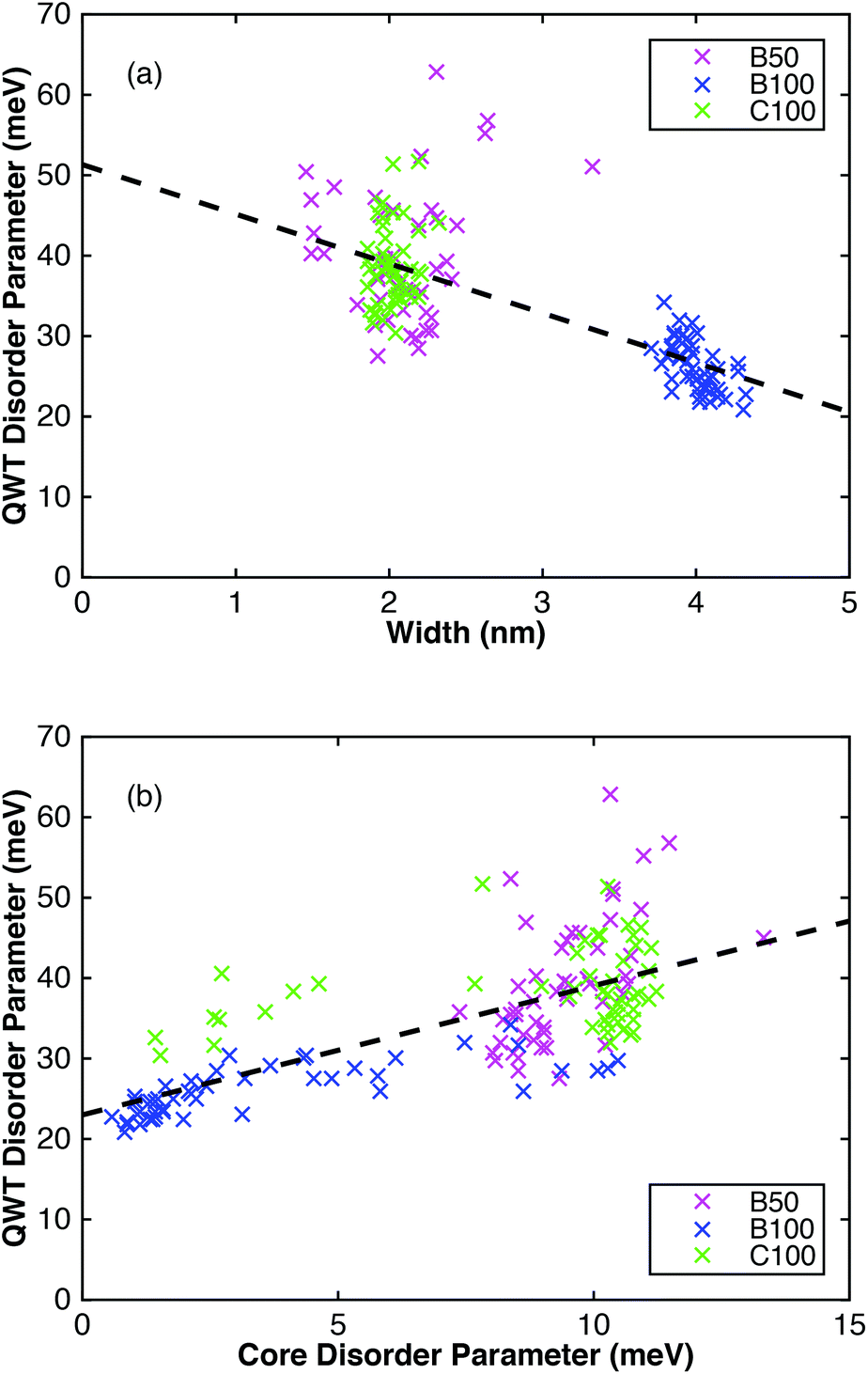 | ||
| Fig. 3 (a) Correlation of the disorder parameter in the QWT with the width of the well. (b) Correlation of the disorder parameter in the QWT with the disorder in the core. The dashed lines in both graphs show a linear least-squares fit of the data. | ||
Fig. 3 also highlights the importance of taking single nanowire measurements, as for sample B50, the inter-wire standard deviation of the QWT energy gap is approximately 60 meV, which is greater than the disorder of a single nanowire (∼40 meV). This spread in QWT energy gap would have presented itself as a larger disorder had ensemble PL measurements been taken, emphasising the value of single nanowire measurements. It is important to note that both the core and the QWT have low disorder on the order of kBT, showing great promise for use in optoelectronic devices. However, efforts to reduce the disorder are often restricted by the FWHM of the emission spectrum being dominated by thermal broadening.47Fig. 3b shows a correlation between the core disorder parameter and the QWT disorder parameter. It is possible that if the core has poor morphology this could be propagated through to the QWT having poor morphology. This gives incentive to produce nanowires with the best core quality possible, even if only the shell layers of the nanowire are the functional elements. Fig. 3b also shows that the disorder of the quantum well tube, σQWT, is consistently larger than the disorder of the core, σCore, with a ratio of σQWT to σCore of 3.9, 6 and 4.1, for the B50, B100 and C100, samples respectively. The larger disorder in the quantum well tube can be attributed to a few factors. Firstly, the much larger surface area to volume ratio of the QWT has an effect. The QWT layer has two boundaries with the Al0.4Ga0.6As barrier layers and is much thinner than the core and is therefore likely to have a higher number of surface states and defects in a given volume. The ratio of the surface area to volume ratio of the quantum well tube to that of the core was 36, 29 and 70, for the B50, B100 and C100 samples, respectively (see ESI†). Secondly, the spectra will also be broadened by different shifts in the QWT energy gap due to varying thicknesses of the QWT in the nanowire. This is confirmed by TEM images (shown in the ESI†) and previous measurements, which show fluctuations of the QWT width around the nanowire.28,48
3.3. Simulations
To further investigate the microscopic origin of the disorder, simulations were performed using a Schrödinger-Poisson solver for semiconductors.49 From these simulations, the band structure and PL were modelled and then compared with experiment. Simulation results for a defect-free nanowire, with a 50 nm core and a QWT width of 4 nm, are presented in Fig. 4. Charge carriers were generated uniformly in the nanowire, with the lattice temperature set to room temperature, and simulations were calculated for a stationary state (further detail is provided in the ESI†). Fig. 4a shows the band structure and charge carrier density taken along a line perpendicular to the nanowire axis. The distribution of electrons and holes in the nanowire heterostructure are influenced by band bending, as a result of Fermi level pinning at the surface; fewer holes than electrons are present in the core, which are accounted for by an excess of electrons in the QWT. The calculated electron (hole) density over a nanowire cross-section is displayed in the left (right) of Fig. 4b. From the numerical calculations, we obtain values for eigenenergies Ee and Eh, and the occupancy of electrons and holes, ne and nh, in these states. Using Fermi's golden rule,50,51 we then compute an approximate emission spectrum, I(E), given by,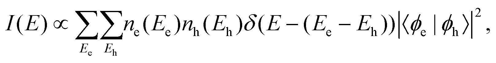 | (5) |
 | ||
| Fig. 4 Vertical grey lines act as a guide for the eye signifying different shell layers. (a) Red and blue lines show the band structure for the conduction band (CB) and valence band (VB) respectively. The two dotted lines show the electron and hole quasi Fermi levels for an excited state. (b) 2D colour plot of the density of electrons (left) and the density of holes (right) for a cross section of the nanowire in an excited state. (c) Charge carrier densities of the electrons and holes in an excited state. There is a slight band bending present giving rise to a difference in distributions for the electrons in the conduction band and holes in the valence band. | ||
 | ||
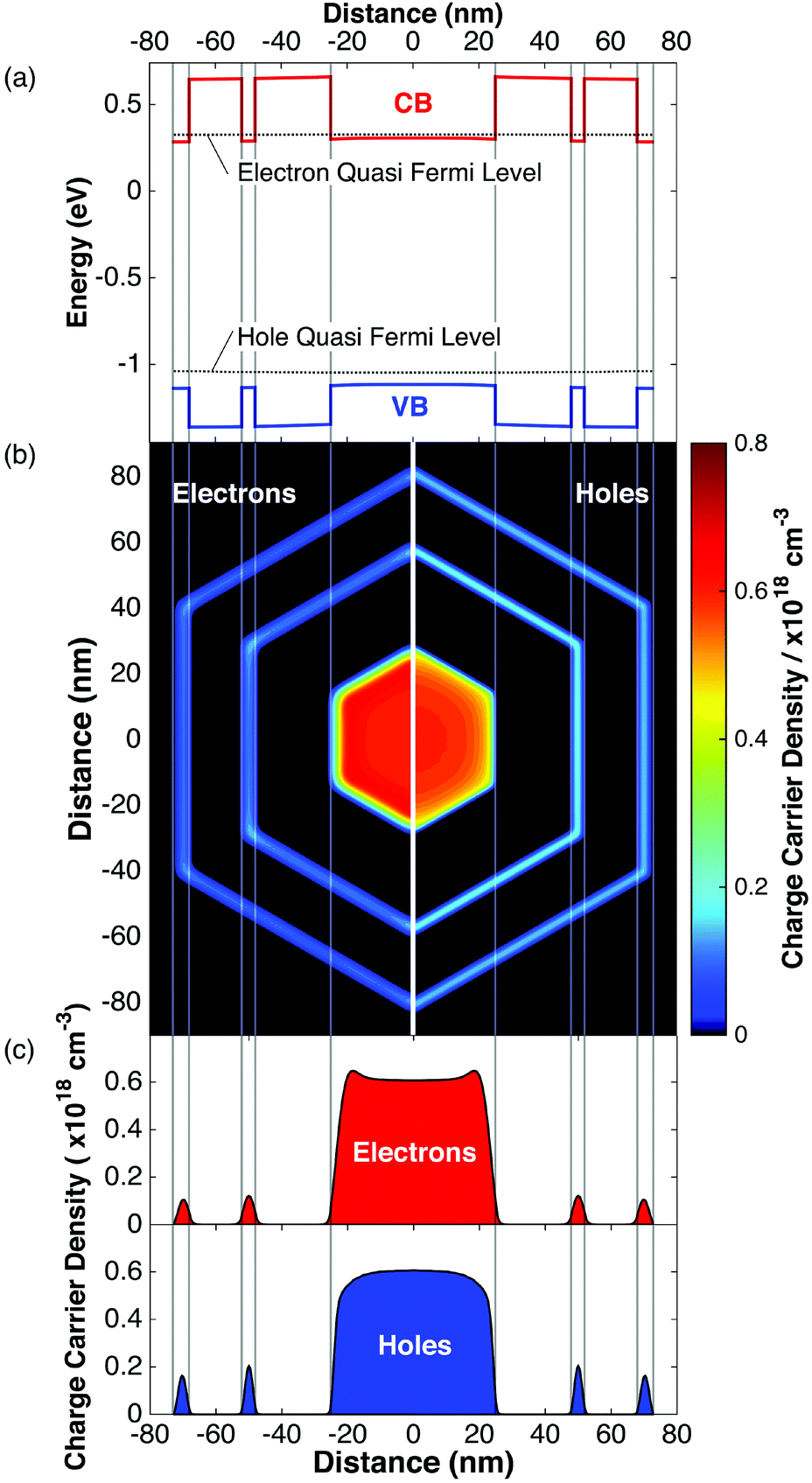
| Fig. 5 (a) Simulated PL of a selection of nanowires with different well widths ranging from 1.5 nm to 4 nm in increments of 0.5 nm. The inset shows the energy shift of the ground state due to confinement as a function of well width. The black crosses are from the simulation results and the red line is from the 1D analytical model. (b) The green lines show simulated PL from a nanowire core (Ideal: 50 nm; disordered: 50 ± 2 nm) and the magenta lines show simulated PL from a QWT (Ideal: 3.5 nm; disordered: 3.5 ± 0.5 nm). The lower plot is for a nanowire with an ideal hexagon geometry. The upper plot is for a nanowire, whose geometry was distorted from a regular hexagon. The insets in (b) show the geometry of the nanowire (not to scale). GaAs and AlGaAs materials are shown in black and white respectively. | ||
We now consider the effect of variations of the QWT width on nanowire facets and relate this to the broadening of single nanowire PL spectra. It has been shown previously28,48 that QWT growth can be enhanced on some facets of a nanowire, leading to a reduction in symmetry of the QWT about the long axis of the nanowire. Indeed, these effects can be observed in TEM micrographs of the nanowires used in this study (see ESI†). In order to investigate the effect of such inhomogeneous well widths on nanowire PL, two different geometries were simulated: an “ideal” nanowire with uniform QWT thickness of 3.5 nm; and a “disordered” nanowire with facet thicknesses varying from 3 to 4 nm. The simulation results are presented in Fig. 5b. It can be seen that PL emission from the core (lower energy peak) is largely unaffected by geometric distortions; however, PL from the QWT is significantly broadened by disorder. This sensitivity to geometric distortions is confirmed by our experimental results (presented in Fig. 3), and indicates why the disorder parameter for the QWT is much larger than that of the core.
4. Conclusion
In conclusion, photoluminescence spectra from 150 individual core–multishell GaAs/Al0.4Ga0.6As nanowires were measured and a statistical analysis performed. This allowed inter-sample and intra-sample variations in QWT width and disorder to be examined. Quantum confinement effects were observed for all nanowire spectra with two clearly defined peaks being attributed to luminescence from the nanowire core and QWT. The QWT widths were calculated from the PL spectra using a finite well model, and confirmed using a full 2D simulation. The disorder for the QWT was quantified by modelling the shape of PL spectra. Disorder was found to be consistently larger in the QWT (40 ± 10 meV) than in the core (8 ± 2 meV) owing to the sensitivity of PL emission energy on variations of QWT width. Correlations between the disorder in the core and QWT are consistent with defects from the core propagating to the QWT and highlights the importance of high quality core growth in the quest for more uniform QWTs. We have demonstrated that measurements of well widths and disorder using room temperature PL spectra can be a useful method to characterise nanowires containing quantum wells. This shows the suitability of the single nanowire PL technique for assessing the quality and uniformity of nanowires prior to their implementation in devices.Acknowledgements
The authors thank the EPSRC (U.K.) and Australian Research Council for financial support. The Australian National Fabrication Facility; ACT node, is acknowledged for access to the growth facility used in this work.References
- M. Yao, N. Huang, S. Cong, C. Y. Chi, M. A. Seyedi, Y. T. Lin, Y. Cao, M. L. Povinelli, P. D. Dapkus and C. Zhou, Nano Lett., 2014, 14, 3293–3303 CrossRef CAS PubMed.
- Y. Qu and X. Duan, J. Mater. Chem., 2012, 22, 16171–16181 RSC.
- K. Peng, P. Parkinson, L. Fu, Q. Gao, N. Jiang, Y.-N. Guo, F. Wang, H. J. Joyce, J. L. Boland, H. H. Tan, C. Jagadish and M. B. Johnston, Nano Lett., 2015, 15(1), 206–210 CrossRef CAS PubMed.
- M. S. Vitiello, L. Viti, L. Romeo, D. Ercolani, G. Scalari, J. Faist, F. Beltram, L. Sorba and A. Tredicucci, Appl. Phys. Lett., 2012, 100, 241101 CrossRef.
- L. Romeo, D. Coquillat, M. Pea, D. Ercolani, F. Beltram, L. Sorba, W. Knap, A. Tredicucci and M. S. Vitiello, Nanotechnology, 2013, 24, 214005 CrossRef CAS PubMed.
- Y. Cui, Z. Zhong, D. Wang, W. U. Wang and C. M. Lieber, Nano Lett., 2003, 3, 149–152 CrossRef CAS.
- G. Liang, J. Xiang, N. Kharche, G. Klimeck, C. M. Lieber and M. Lundstrom, Nano Lett., 2007, 7, 642–646 CrossRef CAS PubMed.
- G. Zheng, F. Patolsky, Y. Cui, W. U. Wang and C. M. Lieber, Nat. Biotechnol., 2005, 23, 1294–1301 CrossRef CAS PubMed.
- Y.-H. Ra, R. Navamathavan, H.-I. Yoo and C.-R. Lee, Nano Lett., 2014, 14, 1537–1545 CrossRef CAS PubMed.
- C. Pan, L. Dong, G. Zhu, S. Niu, R. Yu, Q. Yang, Y. Liu and Z. L. Wang, Nat. Photonics, 2013, 7, 752–758 CrossRef CAS.
- O. L. Muskens, S. L. Diedenhofen, M. H. M. van Weert, M. T. Borgström, E. P. A. M. Bakkers and J. G. Rivas, Adv. Funct. Mater., 2008, 18, 1039–1046 CrossRef CAS.
- T. Kuykendall, P. Ulrich, S. Aloni and P. Yang, Nat. Mater., 2007, 6, 951–956 CrossRef CAS PubMed.
- P. Mohan, J. Motohisa and T. Fukui, Appl. Phys. Lett., 2006, 88, 133105 CrossRef.
- K. Tomioka, J. Motohisa, S. Hara, K. Hiruma and T. Fukui, Nano Lett., 2010, 10, 1639–1644 CrossRef CAS PubMed.
- T. J. Kempa, J. F. Cahoon, S.-K. Kim, R. W. Day, D. C. Bell, H.-G. Park and C. M. Lieber, Proc. Natl. Acad. Sci. U. S. A., 2012, 109, 1407–1412 CrossRef CAS PubMed.
- L. J. Lauhon, M. S. Gudiksen, D. Wang and C. M. Lieber, Nature, 2002, 420, 57–61 CrossRef CAS PubMed.
- S. A. Dayeh, A. V. Gin and S. T. Picraux, Appl. Phys. Lett., 2011, 98, 163112 CrossRef.
- D. Saxena, S. Mokkapati, P. Parkinson, N. Jiang, Q. Gao, H. H. Tan and C. Jagadish, Nat. Photonics, 2013, 7, 963–968 CrossRef CAS.
- F. Qian, S. Gradečak, Y. Li, C.-Y. Wen and C. M. Lieber, Nano Lett., 2005, 5, 2287–2291 CrossRef CAS PubMed.
- J. Wallentin, N. Anttu, D. Asoli, M. Huffman, I. Åberg, M. H. Magnusson, G. Siefer, P. Fuss-Kailuweit, F. Dimroth, B. Witzigmann, H. Q. Xu, L. Samuelson, K. Deppert and M. T. Borgström, Science, 2013, 339, 1057–1060 CrossRef CAS PubMed.
- F. Qian, Y. Li, S. Gradecak, H.-G. Park, Y. Dong, Y. Ding, Z. L. Wang and C. M. Lieber, Nat. Mater., 2008, 7, 701–706 CrossRef CAS PubMed.
- R. Yan, D. Gargas and P. Yang, Nat. Photonics, 2009, 3, 569–576 CrossRef CAS.
- T. Shi, H. E. Jackson, L. M. Smith, N. Jiang, Q. Gao, H. H. Tan, C. Jagadish, C. Zheng and J. Etheridge, Nano Lett., 2015, 15, 1876–1882 CrossRef CAS PubMed.
- M. Fickenscher, T. Shi, H. E. Jackson, L. M. Smith, J. M. Yarrison-Rice, C. Zheng, P. Miller, J. Etheridge, B. M. Wong, Q. Gao, S. Deshpande, H. H. Tan and C. Jagadish, Nano Lett., 2013, 13, 1016–1022 CrossRef CAS PubMed.
- D. Lindgren, K. Kawaguchi, M. Heurlin, M. T. Borgström, M.-E. Pistol, L. Samuelson and A. Gustafsson, Nanotechnology, 2013, 24, 225203 CrossRef PubMed.
- H. J. Joyce, Q. Gao, H. H. Tan, C. Jagadish, Y. Kim, X. Zhang, Y. Guo and J. Zou, Nano Lett., 2007, 7, 921–926 CrossRef CAS PubMed.
- N. Jiang, Q. Gao, P. Parkinson, J. Wong-Leung, S. Mokkapati, S. Breuer, H. H. Tan, C. L. Zheng, J. Etheridge and C. Jagadish, Nano Lett., 2013, 13, 5135–5140 CrossRef CAS PubMed.
- N. Jiang, J. Wong-Leung, H. J. Joyce, Q. Gao, H. H. Tan and C. Jagadish, Nano Lett., 2014, 14, 5865–5872 CrossRef CAS PubMed.
- S. Mokkapati, D. Saxena, N. Jiang, P. Parkinson, J. Wong-Leung, Q. Gao, H. H. Tan and C. Jagadish, Nano Lett., 2012, 12, 6428–6431 CrossRef CAS PubMed.
- A. B. Greytak, C. J. Barrelet, Y. Li and C. M. Lieber, Appl. Phys. Lett., 2005, 87, 151103 CrossRef.
- G. Bulgarini, M. E. Reimer, M. Bouwes Bavinck, K. D. Jöns, D. Dalacu, P. J. Poole, E. P. A. M. Bakkers and V. Zwiller, Nano Lett., 2014, 14, 4102–4106 CrossRef CAS PubMed.
- D. Saxena, F. Wang, Q. Gao, S. Mokkapati, H. H. Tan and C. Jagadish, Nano Lett., 2015, 15(8), 5342–5348 CrossRef CAS PubMed.
- A. V. Senichev, V. G. Talalaev, I. V. Shtrom, H. Blumtritt, G. E. Cirlin, J. Schilling, C. Lienau and P. Werner, ACS Photonics, 2014, 1, 1099–1106 CrossRef CAS.
- K. Hiruma, K. Tomioka, P. Mohan, L. Yang, J. Noborisaka, B. Hua, A. Hayashida, S. Fujisawa, S. Hara, J. Motohisa and T. Fukui, J. Nanotechnol., 2012, 2012, 1–29 CrossRef.
- A. Leitenstorfer, C. Fürst, A. Laubereau, W. Kaiser, G. Tränkle and G. Weimann, Phys. Rev. Lett., 1996, 76, 1545–1548 CrossRef CAS PubMed.
- W. H. Knox, R. L. Fork, M. C. Downer, D. A. B. Miller, D. S. Chemla, C. V. Shank, A. C. Gossard and W. Wiegmann, Phys. Rev. Lett., 1985, 54, 1306–1309 CrossRef CAS PubMed.
- L. Ahtapodov, J. Todorovic, P. Olk, T. Mjå land, P. Slåttnes, D. L. Dheeraj, A. T. J. van Helvoort, B. r.-O. Fimland and H. Weman, Nano Lett., 2012, 12, 6090–6095 CrossRef CAS PubMed.
- G. Zhang, K. Tateno, H. Sanada, T. Tawara, H. Gotoh and H. Nakano, Appl. Phys. Lett., 2009, 95, 123104 CrossRef.
- I. Zelinka, P. N. Suganthan, G. Chen, V. Snášel, A. Abraham and O. Rössler, Nostradamus 2014: Prediction, Modeling and Analysis of Complex Systems, Springer, 2014 Search PubMed.
- M. Patriarca, A. Chakraborti, K. Kaski and G. Germano, Econophysics of Wealth Distributions SE - 10, Springer Milan, 2005, pp. 93–110 Search PubMed.
- M. Montazeri, H. E. Jackson, L. M. Smith, J. M. Yarrison-Rice, J.-H. Kang, Q. Gao, H. H. Tan and C. Jagadish, Nano Lett., 2012, 12, 5389–5395 CrossRef CAS PubMed.
- Y. Wang, H. E. Jackson, L. M. Smith, T. Burgess, S. Paiman, Q. Gao, H. H. Tan and C. Jagadish, Nano Lett., 2014, 14, 7153–7160 CrossRef CAS PubMed.
- V. Dhaka, J. Oksanen, H. Jiang, T. Haggren, A. Nykänen, R. Sanatinia, J.-P. Kakko, T. Huhtio, M. Mattila, J. Ruokolainen, S. Anand, E. Kauppinen and H. Lipsanen, Nano Lett., 2013, 13, 3581–3588 CrossRef CAS PubMed.
- M. Hocevar, L. T. Thanh Giang, R. Songmuang, M. den Hertog, L. Besombes, J. Bleuse, Y.-M. Niquet and N. T. Pelekanos, Appl. Phys. Lett., 2013, 102, 191103 CrossRef.
- Y. Chen, R. Cingolani, L. C. Andreani, F. Bassani and J. Massies, Il Nuovo Cimento D, 1988, 10, 847–859 CrossRef.
- T. Voss, C. Bekeny, L. Wischmeier, H. Gafsi, S. Börner, W. Schade, A. C. Mofor, A. Bakin and A. Waag, Appl. Phys. Lett., 2006, 89, 182107 CrossRef.
- T. Westover, R. Jones, J. Y. Huang, G. Wang, E. Lai and a. A. Talin, Nano Lett., 2009, 9, 257–263 CrossRef CAS PubMed.
- C. Zheng, J. Wong-Leung, Q. Gao, H. H. Tan, C. Jagadish and J. Etheridge, Nano Lett., 2013, 13, 3742–3748 CrossRef CAS PubMed.
- S. Birner, T. Zibold, T. Andlauer, T. Kubis, M. Sabathil, A. Trellakis and P. Vogl, IEEE Trans. Electron Devices, 2007, 54, 2137–2142 CrossRef CAS.
- E. Fermi, Nuclear Physics: A Course Given by Enrico Fermi at the University of Chicago, University of Chicago Press, 1950 Search PubMed.
- F. Rossi, Physica Status Solidi C, 2008, 5, 35–38 CrossRef CAS.
Footnote |
| † Electronic supplementary information (ESI) available: A full description of the modelling used to obtain well widths along with TEM images. See DOI: 10.1039/C5NR06996C |
| This journal is © The Royal Society of Chemistry 2015 |