 Open Access Article
 This Open Access Article is licensed under a
 Creative Commons Attribution 3.0 Unported Licence
Poly(imide-benzoxazole) gate insulators with high thermal resistance for solution-processed flexible indium-zinc oxide thin-film transistors†
Duyoung
Wee‡
a,
Sungmi
Yoo‡
ab,
Young Hun
Kang
a,
Yun Ho
Kim
a,
Jae-Won
Ka
*a,
Song Yun
Cho
a,
Changjin
Lee
a,
Juwhan
Ryu
b,
Mi Hye
Yi
a and
Kwang-Suk
Jang
*a
aDivision of Advanced Materials, Korea Research Institute of Chemical Technology, Daejeon 305-600, Republic of Korea. E-mail: kjang@krict.re.kr; jwka@krict.re.kr
bDepartment of Polymer Science and Engineering, Chungnam National University, Daejeon 305-764, Republic of Korea
First published on 5th June 2014
Abstract
We prepared a poly(imide-benzoxazole) gate insulator for solution-processed flexible metal oxide thin-film transistors (TFTs). The electrical insulating property of the poly(imide-benzoxazole) gate insulator is maintained up to at least 350 °C. The 350 °C-annealed indium-zinc oxide (IZO) TFT with the poly(imide-bezoxazole) gate insulator showed excellent TFT performance with the field-effect mobility of 9.2 cm2 V−1 s−1 and the on/off current ratio of 1.5 × 10⁶. A flexible IZO TFT with the poly(imide-bezoxazole) gate insulator was also fabricated directly on a flexible Kapton substrate. The flexible IZO TFT with the poly(imide-bezoxazole) gate insulator could be operated during bending. Before bending, the mobility and on/off current ratio were 4.1 cm2 V−1 s−1 and 4.7 × 10⁵, respectively. During bending with a radius of 10 mm, the mobility was maintained and the on/off current ratio was slightly decreased to 3.2 × 10⁵.
Introduction
Recently, a great deal of attention has been paid to polymeric gate insulators for solution-processed flexible thin-film transistor (TFT) arrays and circuits.1–9 For low-cost and flexible electronics applications, solution-processable and flexible gate insulators should be used instead of SiO2 gate insulators, prepared on Si substrates by vacuum deposition. Because polymeric gate insulators can be easily printed on flexible substrates at low temperature, they are an attractive candidate for solution-processed flexible TFTs. A variety of high-performance, solution-processed flexible organic TFTs with polymeric gate insulators have been reported.1–7 However, there has been limited research on solution-processed flexible metal oxide TFTs with polymeric gate insulators.Solution-processed metal oxide TFTs with SiO2 gate insulators have shown excellent performance with high field-effect mobility.10–16 In general, metal oxide semiconductors on SiO2 gate insulators are annealed at 200–500 °C to form a coherent interface between the semiconductor and the gate insulator.10–16 To use polymeric gate insulators for solution-processed metal oxide TFTs, they should be compatible with the process for metal oxide semiconductor layers. For example, in bottom-gate TFTs, polymeric gate insulators should not be damaged during the post-annealing process for metal oxide semiconductors, and they should provide a compatible interface to metal oxide semiconductors to form a high-performance active layer. Solution-processed bottom-gate metal oxide TFTs with polymer gate insulators have been inactive or have exhibited poor performance. Moon et al. reported that polymeric gate insulators such as poly(4-vinylphenol), poly(methyl methacrylate), polyimide, and poly(vinyl alcohol) gate insulators are damaged during the post-annealing process of ZnO semiconductor layers for bottom-gate TFTs.17 Kim et al. reported that a solution-processed bottom-gate zinc oxide TFT with a cross-linked poly(4-vinylphenol) gate insulator, prepared on a flexible PET substrate, exhibited mobility of 0.13 cm2 V−1 s−1.9 Recently, we reported the surface modification of high-heat-resistant polyimide gate insulators with an yttrium oxide interlayer for aqueous-solution-processed bottom-gate ZnO TFTs.18 By introduction of the interlayer, a coherent interface between the ZnO semiconductor and the bilayer gate insulator could be obtained. Because an additional interlayer deposition process is required and the obtained field-effect mobility of the ZnO TFT is only 0.456 cm2 V−1 s−1, the process and the TFT performance still need to be improved. (In the case of a top-gate structure, Qiu et al. reported that solution-processed top-gate zinc–tin oxide TFTs with poly(methyl methacrylate) gate insulators exhibited mobilities up to 1.8 cm2 V−1 s−1.19)
In this study, we have developed poly(imide-bezoxazole) (K-PIB) gate insulators with high thermal resistance. The electrical insulating property of the K-PIB was maintained up to 350 °C. To the best of our knowledge, this is the first report on the polymeric gate insulator with high thermal resistance applicable to solution-processed bottom-gate metal oxide TFTs. The K-PIB gate insulators provide a compatible interface to solution-processed indium-zinc oxide (IZO) semiconductors without any interlayers. Solution-processed bottom-gate IZO TFTs with K-PIB gate insulators showed excellent TFT performance with the field-effect mobility of 9.2 cm2 V−1 s−1 and the on/off current ratio of 1.5 × 10⁶. We also fabricated flexible IZO TFTs with the K-PIB gate insulator on a flexible Kapton substrate, which showed excellent TFT performance with the field-effect mobility of 4.1 cm2 V−1 s−1 and the on/off current ratio of 4.7 × 10⁵. Interestingly, during bending with a bending radius of 10 mm, the mobility of the flexible IZO TFT was maintained and the on/off current ratio was slightly decreased to 3.2 × 10⁵.
Results and discussion
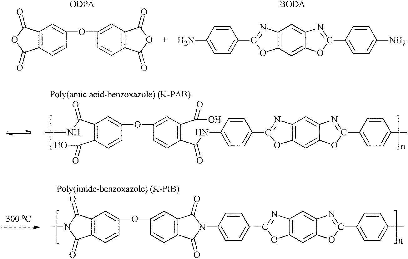
We prepared the K-PIB precursor, poly(amic acid-benzoxazole) (K-PAB), from a dianhydride monomer of 4,4′-oxydiphthalic dianhydride (ODPA) and a rigid aromatic diamine monomer with benzoxazole groups (BODA), as shown in Scheme 1. The viscosity of the polymerization solution with a solid content of 20 wt% reaches the saturation point, 45![[thin space (1/6-em)]](https://www.rsc.org/images/entities/char_2009.gif) 000 cps. The inherent viscosity of K-PAB was found to be 1.03 dL g−1. The prepared K-PAB/dimethylacetamide (DMAc) polymerization solution was directly spin-coated on the indium tin oxide (ITO) glass, and thermally imidized on a hot-plate in ambient air to obtain K-PIB thin films. Weight loss of the K-PAB due to the thermal imidization was observed by thermal gravimetric analysis (TGA) (Fig. 1). The imidization temperature was found to be <300 °C. The weight loss between 120 °C and 300 °C was measured to be 5.3%, which corresponds to the calculated mass difference between the repeat unit masses of K-PAB and K-PIB. The weight loss at a temperature above 550 °C is thought to be due to the carbonization of polymers.20–22 The thermal imidization of K-PAB was also confirmed by IR analysis. The characteristic absorption bands at 1357 cm−1 and 1505 cm−1 are the characteristic imide II band (νC–N) and the aromatic ring stretching band (νC
000 cps. The inherent viscosity of K-PAB was found to be 1.03 dL g−1. The prepared K-PAB/dimethylacetamide (DMAc) polymerization solution was directly spin-coated on the indium tin oxide (ITO) glass, and thermally imidized on a hot-plate in ambient air to obtain K-PIB thin films. Weight loss of the K-PAB due to the thermal imidization was observed by thermal gravimetric analysis (TGA) (Fig. 1). The imidization temperature was found to be <300 °C. The weight loss between 120 °C and 300 °C was measured to be 5.3%, which corresponds to the calculated mass difference between the repeat unit masses of K-PAB and K-PIB. The weight loss at a temperature above 550 °C is thought to be due to the carbonization of polymers.20–22 The thermal imidization of K-PAB was also confirmed by IR analysis. The characteristic absorption bands at 1357 cm−1 and 1505 cm−1 are the characteristic imide II band (νC–N) and the aromatic ring stretching band (νC![[double bond, length as m-dash]](https://www.rsc.org/images/entities/char_e001.gif) C), respectively. Fig. 2 shows the annealing temperature-dependent (a) IR spectrum and (b) νC–N and νCC IR absorbance ratio of the K-PIB films. Because the absorbance ratio, which is proportional to the degree of imidization, is saturated at 250 °C, it is expected that K-PAB films could be fully imidized at above 250 °C. Based on the TGA and IR analysis, an annealing temperature of 300 °C was used for the imidization of K-PAB films in this work. K-PIB imidized at 300 °C showed excellent thermal resistance. The 1% weight-loss temperature of the K-PIB was measured to be 528 °C (Fig. 1), which is higher than the conventional processing temperature of metal oxide semiconductors.
C), respectively. Fig. 2 shows the annealing temperature-dependent (a) IR spectrum and (b) νC–N and νCC IR absorbance ratio of the K-PIB films. Because the absorbance ratio, which is proportional to the degree of imidization, is saturated at 250 °C, it is expected that K-PAB films could be fully imidized at above 250 °C. Based on the TGA and IR analysis, an annealing temperature of 300 °C was used for the imidization of K-PAB films in this work. K-PIB imidized at 300 °C showed excellent thermal resistance. The 1% weight-loss temperature of the K-PIB was measured to be 528 °C (Fig. 1), which is higher than the conventional processing temperature of metal oxide semiconductors.
 | ||
| Scheme 1 Synthetic route to a K-PIB gate insulator. | ||
 | ||
| Fig. 1 TGA results of K-PAB and K-PIB. | ||
 | ||
| Fig. 2 Annealing temperature-dependent (a) IR spectrum and (b) νC–N and νCC IR absorbance ratio of K-PIB films. | ||
Using the metal–insulator–metal (MIM) capacitor structure, the capacitance was measured (Fig. 3a). The capacitance and dielectric constant of the 500 nm-thick K-PIB film were 48.2–50.8 pF mm−2 and 2.7–2.8, respectively, in the frequency range from 40 Hz to 100 kHz. The 500 nm-thick K-PIB film had a smooth surface, as shown in the atomic force microscopy (AFM) image (Fig. 3b). The surface root-mean-square (rms) roughness, calculated from the AFM image (5 μm × 5 μm) of the K-PIB film, was 0.82 nm. The surface energy of the K-PIB film, calculated from the contact angles of water and diiodomethane, was 50.4 dyn cm−1.
 | ||
| Fig. 3 (a) Frequency-dependent capacitance and (b) AFM image (5 μm × 5 μm) of the 500 nm-thick K-PIB film. | ||
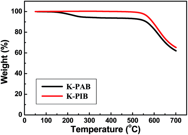
To use the K-PIB film as a gate insulator for solution-processed metal oxide TFTs, its electrical insulating properties after the post-annealing process should be confirmed. The prepared 500 nm-thick K-PIB films were additionally annealed at 300 °C, 350 °C and 400 °C, respectively, for 2 h on a hot-plate in ambient air. Fig. 4 shows the electric field-dependent leakage current densities of 500 nm-thick K-PIB films after post-annealing at 300 °C, 350 °C and 400 °C. The 300 °C and 350 °C-annealed K-PIB films showed excellent insulating properties. The leakage current densities of both the films were measured to be less than 2.3 × 10⁻¹⁰ A cm−2 while biased from 0 to 1.8 MV cm−1. However, after annealing at 400 °C, the leakage current density of the K-PIB film dramatically increased. The leakage current density was measured to be 1.2 × 10⁻⁵ A cm−2 at 1.8 MV cm−1. Although there is no weight loss at 400 °C in the TGA result, the heat treatment could affect the electrical insulating property of K-PIB. It is expected that K-PIB is stable up to at least 350 °C and applicable to solution-processed metal oxide TFTs in terms of thermal stability and electrical insulating property.
 | ||
| Fig. 4 Electric field-dependent leakage current densities of 500 nm-thick K-PIB films after post-annealing at 300 °C, 350 °C and 400 °C. | ||
For comparison, we also prepared the polyimide (K-PI) precursor, the poly(amic acid) (K-PAA) from a dianhydride monomer of ODPA and a diamine monomer of p-phenylenediamine (p-PDA) instead of BODA (Scheme S2†). Fig. S1† shows the electric field-dependent leakage current densities of 300 °C, 350 °C and 400 °C-annealed 500 nm-thick K-PI films. While biased from 0 to 1.8 MV cm−1, the leakage current density of the 300 °C-annealed K-PI film was measured to be less than 3.7 × 10⁻⁶ A cm−2, which is much higher than that of the 300 °C-annealed K-PIB film. There is no weight loss of K-PI at 350 °C and at 400 °C (Fig. S2†). However, electrical breakdown was observed in the 350 °C and 400 °C-annealed K-PI films. Polyimides are well-known to have excellent thermal stability and electrical insulating property that are strongly related to the chain packing.23–25 Use of the BODA with a longer rigid core as a diamine monomer might be advantageous to the polymer chain packing, and it might affect the thermal stability and gate insulating property of the polymer film.
To investigate the potential of the K-PIB film as a gate insulator, solution-processed IZO TFTs with K-PIB gate insulators on a glass substrate or a flexible Kapton substrate were fabricated. Solution-processed IZO TFTs are known to have excellent TFT performance and long-term stability in amorphous structures. We chose a recently reported simple method for the amorphous IZO deposition in which the precursor solution is composed of zinc nitrate, indium acetylacetonate and 2-methoxyethanol.16 Cho et al. reported that 350 °C-annealed IZO TFTs with SiO2 gate insulators exhibited mobilities up to 13.8 cm2 V−1 s−1.16 Although amorphous IZO channel layers with a smooth surface were well-formed on SiO2 gate insulators, the formation on K-PIB gate insulators should be confirmed for the TFT application.
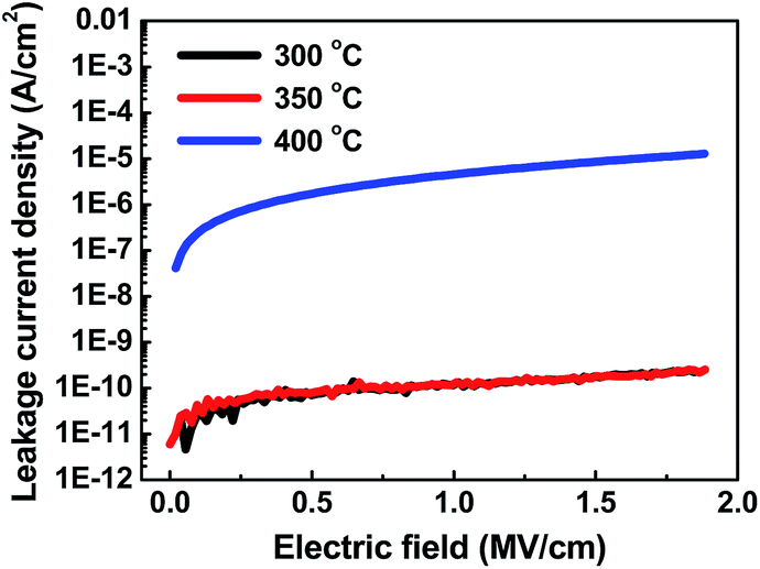
The chemical structure of the IZO layer on the K-PIB gate insulator was studied by X-ray photoelectron spectroscopy (XPS) to verify the formation of the oxide skeleton framework. Fig. 5a shows the O 1s XPS spectra of the 350 °C-annealed IZO layer on the K-PIB gate insulator. The three XPS peaks centered at 528.8, 530.6, and 531.8 eV indicate an oxide lattice surrounded by In and Zn atoms, an oxygen-deficient lattice, that is, an oxide lattice with an oxygen vacancy, and the oxygen in the hydroxide, respectively.26–29 It is clear that the oxide skeleton forms with the presence of a small amount of hydroxide, which is also observed in the IZO layer on the SiO2 gate insulator.16 The 350 °C-annealed IZO layer on the K-PIB gate insulator is thought to be amorphous as confirmed by X-ray diffraction (XRD) analysis (Fig. S3†). It is reported that the solution-processed IZO thin films showed amorphous nature after annealing at 200–450 °C.11,16,30,31
 | ||
| Fig. 5 (a) XPS spectrum, (b) AFM image (5 μm × 5 μm), (c) SEM image and (d) cross-sectioned TEM image of the IZO layer on the K-PIB film. | ||
Fig. 5b shows an AFM image of the 350 °C-annealed IZO layer on the K-PIB gate insulator. On the K-PIB gate insulator, an IZO layer with a smooth surface was well-formed. The surface rms roughness, measured in an area of 5 μm × 5 μm, was 0.99 nm, which is comparable to that of the K-PIB gate insulator, 0.82 nm. The smooth surface of the IZO layer on the K-PIB gate insulator was also observed by scanning electron microscopy (SEM) (Fig. 5c). Formation of a coherent interface between the IZO semiconductor and the K-PIB gate insulator was confirmed by transmission electron microscopy (TEM) (Fig. 5d and Fig. S4†). An amorphous 5 nm-thick IZO layer on the K-PIB gate insulator was observed in the cross-sectioned TEM images. Formation of the coherent interface might be related to the precursor solution wettability of the K-PIB film and the amorphous nature of the IZO layer. The contact angle of 2-methoxyethanol, the solvent for the IZO precursor solution, on the K-PIB film is less than 5°. The amorphous structure might prevent the formation of pores and cracks during the annealing process.
Fig. 6 shows the transfer characteristics (Idsvs. Vgs) of the 300 °C, 350 °C and 400 °C-annealed IZO TFTs with K-PIB gate insulators. The solution-processed TFTs showed excellent TFT performance. The electrical performance parameters, namely, mobility, on/off current ratio (Ion/Ioff), subthreshold slope (S-slope) and threshold voltage (Vth) are summarized in Table 1. The 300 °C, 350 °C and 400 °C-annealed IZO TFTs with K-PIB gate insulators exhibited mobilities up to 6.0, 9.0 and 11.2 cm2 V−1 s−1, respectively. In general, more complete formation of the M-O-M bonds and higher mobility of the TFTs are expected at the higher annealing temperature of metal oxide semiconductors. However, the off current of the 400 °C-annealed IZO TFT is much higher than those of the 300 °C and 350 °C-annealed IZO TFTs. The higher off current value is due to the reduced electrical insulating property of the K-PIB gate insulator, post-annealed at 400 °C, as shown in Fig. 4. Rolland et al. reported that the upper limit of density of interfacial trap states could be extracted from the subthreshold slope.32 (The calculation method was described elsewhere.32–35) The estimated upper limits of the 300 °C, 350 °C and 400 °C-annealed K-PIB gate insulators are 2.4 × 10¹², 1.0 × 10¹² and 2.3 × 1012 cm−2 eV−1, respectively. Overall, the 350 °C-annealed IZO TFT with the K-PIB gate insulator showed the best performance. To obtain the average and standard deviations of the electrical performance parameters, we prepared twenty 350 °C-annealed IZO TFTs with K-PIB gate insulators (Table 2). The average mobility, threshold voltage, and subthreshold slope were measured to be 5.5 ± 1.5 cm2 V−1 s−1, 24.0 ± 3.8 V, and 3.0 ± 0.8 V per decade, respectively. Also, their on/off current ratios were in the range from 2.3 × 10⁵ to 1.5 × 10⁶. The output characteristics (Idsvs. Vds) of the 350 °C-annealed IZO TFT shows clear linear and saturation regions (Fig. 7).
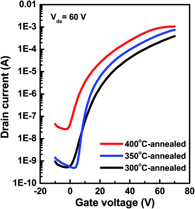 | ||
| Fig. 6 Transfer characteristics (Idsvs. Vgs) of the 300 °C, 350 °C and 400 °C-annealed IZO TFTs with K-PIB gate insulators. | ||
| IZO annealing temperature [°C] | Channel length (L) = 50 μm and channel width (W) = 1000 μm | |||
|---|---|---|---|---|
| Mobility [cm2 V−1 s−1] | I on/Ioff | S-slope [V per decade] | V th [V] | |
| 300 | 6.0 | 7.1 × 10⁵ | 4.6 | 31.3 |
| 350 | 9.2 | 1.5 × 10⁶ | 2.0 | 26.5 |
| 400 | 11.2 | 3.8 × 10⁴ | 4.4 | 18.8 |
| Channel length (L) = 50 μm and channel width (W) = 1000 μm | |||
|---|---|---|---|
| Mobility [cm2 V−1 s−1] | I on/Ioff | S-slope [V per decade] | V th [V] |
| 5.5 ± 1.5 | 2.3 × 10⁵ to 1.5 × 10⁶ | 3.0 ± 0.8 | 24.0 ± 3.8 |
 | ||
| Fig. 7 Output characteristics (Idsvs. Vds) of the 350 °C-annealed IZO TFT. | ||
To verify the feasibility of the solution-processed flexible TFT, we fabricated 350 °C-annealed IZO TFT with the K-PIB gate insulator directly on a 120 μm-thick flexible Kapton substrate (Fig. 8a). The output characteristics (Idsvs. Vds) of the IZO TFT on a Kapton substrate shows clear linear and saturation regions (Fig. 8b). Fig. 8c shows the transfer characteristics (Idsvs. Vgs) of the IZO TFT with the K-PIB gate insulator on a flexible Kapton substrate before bending and during bending with a radius of 10 mm. The flexible TFT shows excellent TFT performance (Table 3). Before bending, the mobility, on/off current ratio, subthreshold slope, and threshold voltage were 4.1 cm2 V−1 s−1, 4.7 × 10⁵, 2.7 V per decade, and 22.8 V, respectively. Interestingly, no significant reduction in TFT performance was observed during bending, as shown in Fig. 8c. During bending with a radius of 10 mm, the mobility, on/off current ratio, subthreshold slope, and threshold voltage were 4.1 cm2 V−1 s−1, 3.2 × 10⁵, 3.0 V per decade, and 23.0 V, respectively. Our results indicate that the IZO TFT with the K-PIB gate insulator can operate during bending. We believe that the K-PIB gate insulator is an attractive candidate for solution-processed flexible metal oxide TFTs.
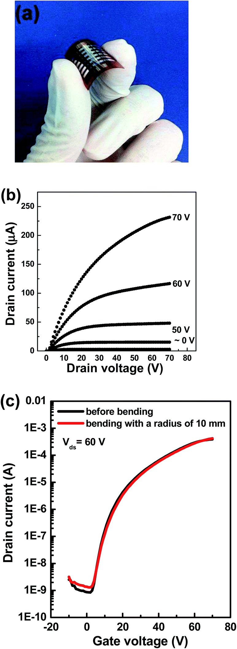 | ||
| Fig. 8 (a) Photograph, (b) output characteristics (Idsvs. Vds) and (c) transfer characteristics (Idsvs. Vgs) of the 350 °C-annealed flexible IZO TFT on a Kapton substrate. | ||
| Bending radius [mm] | Channel length (L) = 50 μm and channel width (W) = 1000 μm | |||
|---|---|---|---|---|
| Mobility [cm2 V−1 s−1] | I on/Ioff | S-slope [V per decade] | V th [V] | |
| ∞ | 4.1 | 4.7 × 10⁵ | 2.7 | 22.8 |
| 10 | 4.1 | 3.2 × 10⁵ | 3.0 | 23.0 |
Conclusion
We report a poly(imide-benzoxazole) gate insulator with high thermal resistance for solution-processed flexible metal oxide TFTs. To investigate the potential of the poly(imide-benzoxazole) as a gate insulator, we fabricated solution-processed IZO TFTs. The 350 °C-annealed IZO TFT with the K-PIB gate insulator showed excellent TFT performance with the field-effect mobility of 9.2 cm2 V−1 s−1 and the on/off current ratio of 1.5 × 10⁶. We also fabricated flexible IZO TFTs with the K-PIB gate insulator, which showed excellent TFT performance with the field-effect mobility of 4.1 cm2 V−1 s−1 and the on/off current ratio of 4.7 × 10⁵. Interestingly, during bending with a bending radius of 10 mm, the TFT performance of the flexible IZO TFT was maintained. Our results indicate that the poly(imide-benzoxazole) gate insulator is applicable for high-performance, solution-processed flexible metal oxide TFTs.Experimental
We prepared a rigid aromatic diamine monomer, BODA, from diaminodihydroxybenzene dihydrochloride (DADHB) and aminobenzoic acid (ABA) for polymerization of the K-PIB (Scheme S1†). Then, 0.011 mol of DADHB was added to 50 g of polyphosphoric acid (PPA). After the solution was vigorously stirred at 100 °C for 2 h, 0.022 mol of ABA was added and the solution was vigorously stirred at 120 °C for 4 h. The solution temperature was raised to 150 °C at a rate of 30 °C h−1 and to 170 °C at a rate of 20 °C h−1. After vigorously stirring for 2 h, 500 ml of DI water was added. The precipitates were washed repeatedly with 5 wt% NaHCO3 aqueous solution and DI water. After the dried product was dissolved in 20 ml of dimethyl sulfoxide, the solution was added dropwise to 500 ml of toluene. The precipitated product was washed with toluene and dried in vacuo at 80 °C.We prepared the K-PIB precursor, the K-PAB from monomers of ODPA and BODA (Scheme 1). In DMAc, 0.01 mol of ODPA and 0.01 mol of BODA were dissolved. The total concentration of the monomers was 20 wt%. The solution was stirred until the solution viscosity reached the saturation point. ITO-coated glass was used as a substrate and the ITO was patterned to produce an electrode with the conventional photolithographic method: coating with a photoresist and ultraviolet light exposure followed by developing and etching. The patterned ITO substrate was cleaned using a typical cleaning process for electronic applications: sonication in detergent, deionized water, acetone, and isopropanol in that order for 20 min at room temperature. The K-PAB solution was spin-coated on patterned ITO-coated glasses. The spin-coated films were annealed at 90 °C for 10 min and 300 °C for 40 min on a hot-plate in ambient air. The final thickness of the K-PIB films was controlled to be 500 nm.
To determine the capacitance and the leakage current density of the gate insulators, MIM capacitor structures were prepared by deposition of the top gold electrode on the gate insulator-coated ITO glass. The active area of the MIM devices was 50.24 mm2. For electrical characterizations, we prepared bottom-gate, top-contact TFT devices. ITO-coated glass or a gold-coated Kapton film was used as a substrate. The ITO and the gold were patterned (2 mm wide stripes) to produce the gate electrode. To prepare the IZO precursor solution, 0.05 M zinc acetylacetonate hydrate (Zn(C5H7O2)2·xH2O) and 0.05 M indium nitrate hydrate (In(NO3)3·xH2O) were dissolved in anhydrous 2-methoxyethanol. After spin-coating of the IZO precursor solution on the K-PIB gate insulator at 4000 rpm for 30 s, the film was annealed at 90 °C for 10 min and 300 °C for 2 h on a hot-plate in ambient air. After the annealing process, a 100 nm-thick aluminum source and drain electrodes were deposited by thermal evaporation on the semiconductor layer through a shadow mask, creating transistors with a channel length (L) and a width (W) of 50 and 1000 μm, respectively.
The capacitance was measured with an Agilent 4294A impedance analyzer. The transfer (Idsvs. Vgs) and output (Idsvs. Vds) characteristics of the TFT s were measured with an Agilent E5272 semiconductor parameter analyzer. All these electrical measurements were carried out in air without any encapsulation. XRD analysis was performed using a thin film diffraction in which samples were fixed at an angle of 3° to the X-ray beam with 2θ scan of the detector. XPS analysis was performed on an AXIS Nova spectrometer (Kratos Analytical) using a monochromatic an Al Kα source (hν = 1486.6 eV) at a power of 140–150 W. The XPS spectrum was obtained without any treatment. The spectrum was recorded applying a pass energy of 40 eV with an energy resolution of 0.8 eV. The analysis spot size was 400 μm × 800 μm and the vacuum below 10−8 Torr for the measurement.
Acknowledgements
This work was supported by a grant from the cooperative R&D program funded by the Korea Research Council for Industrial Science and Technology and was partially supported by the KRICT core project (KK-1402-C0) funded by the Ministry of Knowledge Economy.References
- J. H. Cho, J. Lee, Y. Xia, B. Kim, Y. He, M. J. Renn, T. P. Lodge and C. D. Frisbie, Nat. Mater., 2008, 7, 900 CrossRef CAS PubMed
.
- M. E. Roberts, N. Queroltó, S. C. B. Mannsfeld, B. N. Reinecke, W. Knoll and Z. Bao, Chem. Mater., 2009, 21, 2292 CrossRef CAS
- Z. Liu, J. H. Oh, M. E. Roberts, P. Wei, B. C. Paul, M. Okajima, Y. Nishi and Z. Bao, Appl. Phys. Lett., 2009, 94, 203301 CrossRef PubMed
- S. C. B. Mannsfeld, B. C.-K. Tee, R. M. Stoltenberg, C. V. H.-H. Chen, S. Barman, B. V. O. Muir, A. N. Sokolov, C. Reese and Z. Bao, Nat. Mater., 2010, 9, 859 CrossRef CAS PubMed
- A. Sokolov, Y. Cao, O. B. Johnson and Z. Bao, Adv. Funct. Mater., 2012, 22, 175 CrossRef CAS
- K.-J. Baeg, D. Khim, S.-W. Jung, M. Kang, I.-K. You, D.-Y. Kim, A. Facchetti and Y.-Y. Noh, Adv. Mater., 2012, 24, 5433 CrossRef CAS PubMed
- J.-Y. Yoon, S. Jeong, S. S. Lee, Y. H. Kim, J.-W. Ka, M. H. Yi and K.-S. Jang, ACS Appl. Mater. Interfaces, 2013, 5, 5149 CAS
- P. K. Nayak, J. Kim, C. Lee and Y. Hong, Phys. Status Solidi A, 2010, 207, 1664 CrossRef CAS
- K. Kim, S. Park, J.-B. Seon, K.-H. Lim, K. Char, K. Shin and Y. S. Kim, Adv. Funct. Mater., 2011, 21, 3546 CrossRef CAS
- M.-G. Kim, M. G. Kanatzidis, A. Facchetti and T. J. Marks, Nat. Mater., 2011, 10, 382 CrossRef CAS PubMed
- K. K. Banger, Y. Yamashita, K. Mori, R. L. Peterson, T. Leedham, J. Rickard and H. Sirringhaus, Nat. Mater., 2011, 10, 45 CrossRef CAS PubMed
- S. Jeong, Y.-G. Ha, J. Moon, A. Facchetti and T. J. Marks, Adv. Mater., 2010, 22, 1346 CrossRef CAS PubMed
- S.-Y. Han, G. S. Herman and C.-H. Chang, J. Am. Chem. Soc., 2011, 133, 5166 CrossRef CAS PubMed
- M.-G. Kim, H. S. Kim, Y.-G. Ha, J. He, M. G. Kanatzidis, A. Facchetti and T. J. Marks, J. Am. Chem. Soc., 2010, 132, 10352 CrossRef CAS PubMed
- S. Y. Park, B. J. Kim, K. Kim, M. S. Kang, K.-H. Lim, T. I. Lee, J. M. Myoung, H. K. Baik, J. H. Cho and Y. S. Kim, Adv. Mater., 2012, 24, 834 CrossRef CAS PubMed
- Y. H. Kang, S. Jeong, J. M. Ko, J.-Y. Lee, Y. Choi, C. Lee and S. Y. Cho, J. Mater. Chem. C, 2014, 2, 4247 RSC
- Y. Jung, T. Jun, A. Kim, K. Song, T. H. Yeo and J. Moon, J. Mater. Chem., 2011, 21, 11879 RSC
- K.-S. Jang, D. Wee, Y. H. Kim, J. Kim, T. Ahn, J.-W. Ka and M. H. Yi, Langmuir, 2013, 29, 7143 CrossRef CAS PubMed
- Y. Zhao, G. Dong, L. Duan, J. Qiao, D. Zhang, L. Wang and Y. Qiu, RSC Adv., 2012, 2, 5307 RSC
- M. Inagaki, S. Harada, T. Sato, T. Nakajima, Y. Horino and K. Morita, Carbon, 1989, 27, 253 CrossRef CAS
- M. Inagaki, Carbon, 1991, 29, 1239 CrossRef CAS
- Y. Hishiyama, A. Yoshida and Y. Kaburagi, Carbon, 1992, 30, 333 CrossRef CAS
- T. Ahn, J. W. Kim, Y. Choi and M. H. Yi, Org. Electron., 2008, 9, 711 CrossRef CAS PubMed
- J. Y. Kim, M. H. Yi and T. Ahn, Thin Solid Films, 2010, 518, 6280 CrossRef CAS PubMed
- K.-S. Jang, W. S. Kim, J.-M. Won, Y.-H. Kim, S. Myung, J.-W. Ka, J. Kim, T. Ahn and M. H. Yi, Phys. Chem. Chem. Phys., 2013, 15, 950 RSC
- J. C. C. Fan and J. B. Goodenough, J. Appl. Phys., 1997, 48, 3524 CrossRef PubMed
- S. Major, S. Kumar, M. Bhatnagar and K. L. Chopra, Appl. Phys. Lett., 1986, 49, 394 CrossRef CAS PubMed
- T. Ishida, H. Kobayashi and Y. Nakato, J. Appl. Phys., 1993, 73, 4344 CrossRef CAS PubMed
- E. M. C. Fourunato, L. M. N. Pereira, P. M. C. Barquinha, A. M. Bothlho do Rego, G. Goncalves, A. Vila, J. R. Moran and R. F. P. Martins, Appl. Phys. Lett., 2008, 92, 222103 CrossRef PubMed
- R. C. Hoffmann, M. Kaloumenos, S. Heinschke, E. Erdem, P. Jakes, R.-A. Eichel and J. J. Schneider, J. Mater. Chem. C, 2013, 1, 2577 RSC
- C. Y. Koo, K. Song, T. Jun, D. Kim, Y. Jeong, S.-H. Kim, J. Ha and J. Moon, J. Electrochem. Soc., 2010, 157, J111 CrossRef CAS PubMed
- A. Rolland, J. Richard, J. P. Kleider and D. Mencaraglia, J. Electrochem. Soc., 1993, 140, 3679 CrossRef CAS PubMed
- M. McDowell, I. G. Hill, J. E. McDermott, S. L. Bernasek and J. Schwartz, Appl. Phys. Lett., 2006, 88, 073505 CrossRef PubMed
- A. Petritz, A. Wolfberger, A. Fian, J. R. Krenn, T. Griesser and B. Stadlober, Org. Electron., 2013, 14, 3070 CrossRef CAS PubMed
- J.-Y. Yoon, Y. H. Kim, J.-W. Ka, S.-K. Hong, M. H. Yi and K.-S. Jang, J. Mater. Chem. C, 2014, 2, 2191 RSC
Footnotes |
| † Electronic supplementary information (ESI) available. See DOI: 10.1039/c4tc00709c |
| ‡ These authors contributed equally to this work. |
| This journal is © The Royal Society of Chemistry 2014 |