
 Open Access Article
 This Open Access Article is licensed under a
 Creative Commons Attribution 3.0 Unported Licence
A highly flexible and compact magnetoresistive analytic device†
Gungun
Lin
*a,
Denys
Makarov
*a,
Michael
Melzer
a,
Wenping
Si
ab,
Chenglin
Yan
ac and
Oliver G.
Schmidt
ab
aInstitute for Integrative Nanosciences, IFW Dresden, Helmholtzstr. 20, 01069 Dresden, Germany. E-mail: g.lin@ifw-dresden.de; d.makarov@ifw-dresden.de
bMaterial Systems for Nanoelectronics, Chemnitz University of Technology, Reichenhainer Str. 70, 09107 Chemnitz, Germany
cSchool of Energy, Soochow University, 215006 Suzhou, Jiangsu, People's Republic of China
First published on 27th August 2014
Abstract
A grand vision of realization of smart and compact multifunctional microfluidic devices for wearable health monitoring, environment sensing and point-of-care tests emerged with the fast development of flexible electronics. As a vital component towards this vision, magnetic functionality in flexible fluidics is still missing although demanded by the broad utility of magnetic nanoparticles in medicine and biology. Here, we demonstrate the first flexible microfluidic analytic device with integrated high-performance giant magnetoresistive (GMR) sensors. This device can be bent to a radius of 2 mm while still retaining its full performance. Various dimensions of magnetic emulsion droplets can be probed with high precision using a limit of detection of 0.5 pl, providing broad applicability in high-throughput droplet screening, flow cytometry and drug development. The flexible feature of this analytic device holds great promise in the realization of wearable, implantable multifunctional platforms for biomedical, pharmaceutical and chemical applications.
Introduction
Flexible electronics represent a new generation of devices with exclusive features which conventional electronic devices relying on rigid substrates cannot surpass, i.e., reshaping their original form after fabrication and even intimate contact with arbitrary geometries. Extensive research studies have been reported on stretchable integrated circuits,1,2 bendable batteries,3,4 light-emitting diodes,5 flexible6,7 and stretchable8 magnetoelectronics, rollable electronic displays,9,10 ultrathin transistors,11,12 solar cells,13 and paper-based electronics.14 In recent years, technological developments have been driven from a single functional element towards the realization of more complex integrated platforms. For instance, an active-matrix tactile sensing foil with arrays of integrated switching transistors and touch sensors was demonstrated.11 Moreover, flexible electronics benefited from recent advances in microfluidics, leading to the emergence of a new type of flexible diagnostic device or micro total analysis system (μTAS), which is cost-efficient and suited for resource-limited settings or poverty-related conditions and mechanically flexible, appropriate for wearable, implantable biomedical devices or fluid delivery systems. Flexible microfluidic devices have been reported using a label-free chemical sensing method on cellulose paper,15–17 textiles18 or polymeric substrates.19Nonetheless, the diverse fields of microfluidics have seen extensive applications of magnetic nanoparticles in, i.e., early detection or treatment of cancer,20–22 immunological assays,23 point-of-care tests,24 and on-chip manipulations of biospecies.25,26 Detection of magnetically labelled biomarkers in complex biological samples with GMR,27–34 tunnelling magnetoresistance (TMR)35,36 or hall sensors37 has been realized on rigid platforms based on a microarray format, which is suitable for multiplex diagnostics or assays by detecting magnetic labels statically immobilized on substrates. However, this format is unsuitable for whole cell analyses. Recently, in-flow detection with magnetic sensors based on a cytometric format addressed the need for analyses on a cell level and promised high-throughput enumerations of magnetically labelled entities.38–44 In addition, droplet-based microfluidics encapsulating biological species and magnetic nanoparticles can also benefit from the fast development of magnetic flow detection as emulsion droplets armed with magnetic functionality can be used to transport, mix and release cargos in a controlled manner.25,26 The effective on-chip operation of emulsion droplets, however, relies on a clear identification of their volume and the concentration of encapsulated magnetic nanoparticles. The evaluation of the as-synthesised magnetic microgels in droplet microfluidics primarily relied on optical observations,45 the instant feedback of which is crucial for process control. Therefore, accompanied by the eagerness and development of modern multifunctional biomedical devices that are lightweight, inexpensive, wearable or even implantable, a cost-efficient flexible integrated microfluidic platform combining advantages from flexible electronics and fluidics and possessing magnetic functionalities, i.e., for detection and quantification of magnetic objects in real time, is highly attractive and demanded.
Here, we fabricate the first highly flexible polymer-sandwiched giant magnetoresistive (GMR) device with an integrated continuous microfluidic flow system, which processes magnetic functionality as demanded and is capable of probing magnetic objects encapsulated in emulsion droplets. The volume of droplets loaded with superparamagnetic nanoparticles ranges from hundreds of picoliters to a few nanoliters, which can be well incorporated in lab-on-a-chip devices with a low consumption volume while still providing a sufficient amount of materials for on-chip manipulation. The detection limit for the magnetic content in an emulsion droplet of 1 nl was about 4 mg ml−1, which is perfectly suited for full-range magnetic manipulations of droplets on-chip including magnet disengagement, droplet dispersion and particle extraction.26 The entire device can be bent down to a radius of 2 mm while still maintaining its full performance, which renders it the most flexible microfluidic analytic tool reported so far.
Materials and methods
Preparation of substrates
A layer of SU-8 2 (MicroChem) photosensitive polymer was coated on a PET foil in order to reduce the surface roughness. TI prime (MicroChem) was used as an adhesion promoter, before which a 5 min oxygen plasma treatment at 40 mW was performed to remove adsorbents. The spin-coating speed of SU-8 2 was adjusted to 6000 rpm to produce a layer thickness of about 800 nm. The spin-coated SU-8 2 buffer was baked at 90 °C on a hot plate for 5 min and cross-linked by UV exposure using a mask aligner (Karl Suss, MJB4) followed by post-baking at 90 °C for 5 min.Fabrication of GMR sensors
The sensor was prepared by the magnetron sputtering technique. Before deposition, a negative photoresist (AZ5214E, MicroChem) was spin-coated on a PET foil buffered with an SU-8 2 layer, which was subsequently patterned into a rectangular stripe with dimensions of 6 μm × 100 μm by a standard photolithography technique using image reversal process. The deposition was performed under high vacuum conditions with a base pressure of about 7.0 × 10⁻⁷ mbar. Ar was used as the sputter gas, the pressure of which was kept at 9.4 × 10⁻⁴ mbar. The structure of the sensor was revealed by lifting off the photoresist with acetone. After patterning the GMR sensors, a second-step lithography based on the lift-off process was used to pattern the electrical contacts which were aligned with the sensors. Ta (5 nm)/Cu (200 nm)/Ta (5 nm) were used as the materials for the electrical contacts, which were deposited by the magnetron sputtering technique.Encapsulation of GMR sensors
In order to protect the GMR sensor from current leakage when it is integrated into a microfluidic channel, an SU-8 2 photosensitive polymer of thickness about 700 nm was spin-coated on top of the sensor at a spin speed of 8000 rpm. Afterwards, the SU-8 2 insulation layer was exposed under UV light with a mask aligner (Karl Suss, MJB4) to cross-link the polymers. After exposure, the SU-8 2 layer was left without post-baking to retain epoxy groups in order to facilitate final assembly with a PDMS channel.Assembly of the final device
The PDMS microfluidic channel was prepared based on a mould casting approach. Firstly, a layer of SU-8 50 (MicroChem) polymer was spin-coated on a silicon wafer at a speed of 1000 rpm to obtain a layer thickness of 100 μm. Then, the polymer was patterned by standard photolithography process, resulting in a channel width of 100 μm. A fresh PDMS (Silicone Elastomer KIT, Sylgard 184, Dow Corning) mixture (1![[thin space (1/6-em)]](https://www.rsc.org/images/entities/char_2009.gif) :10 in wt%) was prepared, poured into the SU-8 50 mould and cured at 200° for 5 min. Afterwards, the cured PDMS channel was peeled off from the silicon wafer. The inlets/outlets of the channel were created through PDMS using a biopsy punch with a diameter of 1 mm. The assembly of the device was finalized by bonding the PDMS channel to the SU-8-encapsulated chip. A N2 plasma treatment was carried out for 3 min at 40 mW to produce amine-terminated groups on the PDMS surface.53 Then the chip and the PDMS channel were brought into contact under an optical microscope to precisely align the channel with the sensors. Finally, the device was baked at 120 °C on a hot plate for 30 min to achieve permanent bonding between the PDMS and the chip.
:10 in wt%) was prepared, poured into the SU-8 50 mould and cured at 200° for 5 min. Afterwards, the cured PDMS channel was peeled off from the silicon wafer. The inlets/outlets of the channel were created through PDMS using a biopsy punch with a diameter of 1 mm. The assembly of the device was finalized by bonding the PDMS channel to the SU-8-encapsulated chip. A N2 plasma treatment was carried out for 3 min at 40 mW to produce amine-terminated groups on the PDMS surface.53 Then the chip and the PDMS channel were brought into contact under an optical microscope to precisely align the channel with the sensors. Finally, the device was baked at 120 °C on a hot plate for 30 min to achieve permanent bonding between the PDMS and the chip.
Experimental setup
Magnetoelectrical characterization was performed with a 4-probe geometry in a magnetoelectrical testing station. The GMR sensors were placed in between two pole shoes of the electromagnets, where magnetic fields could be swept between ±30 mT, which was sufficient to saturate the sensor. The GMR sensor was powered by a constant current, while the voltage change was recorded by a programmed multimeter (Keithley Model 2000). The bending experiments were realized on a motor-controlled mechanical loading setup. The sample was mounted on a loading stage, one end of which was precisely driven by a motor to move over a defined distance, while the other end was fixed. Meanwhile, the stage was placed inside the abovementioned magnetoelectrical testing station, from which GMR curves could be measured on samples at different bending states.For the real-time detection of emulsion droplets, a measurement setup was established based on a Wheatstone bridge (see details in the ESI†). The whole bridge was powered by a lock-in amplifier, the differential voltage signal ΔV of which was fed into the lock-in amplifier to improve the signal-to-noise ratio. The analogue output from the lock-in amplifier was picked up by an analogue/digital converter (NI-USB 6800, National Instrument). A constant AC measuring current of 1 mA was used. An internal lock-in sinusoidal signal with a frequency of 1 kHz and an amplitude of 0.08 V was used as a reference. The sampling rate of the AD converter was 5 kHz. The measurement range of the lock-in amplifier was 500 μV. For the measurement, an external permanent magnet was placed below the sensor. As the sensor is sensitive to the in-plane magnetic field, the in-plane component of the stray fields from the magnet was used to bias the sensor to the most sensitive region. The position of the magnet was carefully adjusted via monitoring the sensor output and fixed during the whole measurement of droplets.
Utilized reagents
The substrate used is a transparent, flexible sheet of PET with a thickness of 100 μm. To produce stable magnetic droplets in a microfluidic channel, hydrocarbon oil (Vacuum pump fluid, TKO 19 Ultra, Kurt J. Lesker) mixed with 5 wt% SPAN 80 was used as the continuous phase and magnetic nanoparticles (Ferrotec, EMG 700) diluted with different amounts of DI water were used as the dispersed phase.Results and discussions
Fabrication of the flexible magnetoresistive analytic device
To probe magnetic particles or emulsion droplets in microfluidics, a magnetic sensor with high sensitivity and a small effective sensing area, which is comparable to the dimensions of objects to be detected, is required.46 The signal is essentially related to the effective magnetic stray fields of the magnetic entities that could be detected by a magnetic sensor.42,46 To fulfill the stringent requirements of the sensor sensitivity, high-performance sensing elements relying on the GMR effect should be applied. In this respect, GMR multilayers and spin valve sensors were already successfully fabricated on flexible6,7,47,56 as well as elastic membranes.48,49,57 In the present work, we chose highly sensitive GMR [Py(1.5 nm)/Cu(2.3 nm)]30 multilayers (Py = Ni81Fe19) coupled at the 2nd antiferromagnetic maximum prepared on a transparent, flexible sheet of polyethylene terephthalate (PET). The thickness of PET is 100 μm, which is mechanically stable to sustain high pressure during continuous pumping in a microfluidic channel while still maintaining the advantage for the device of getting reshaped as needed. The fabrication process of a flexible microfluidic magnetic device based on a polymer-sandwiched GMR sensor is displayed in Fig. 1. A strong advantage of the platform on a flexible foil over conventional electronics integrated in microfluidic channels fabricated on silicon or glass substrates is the possibility of fabrication over large areas (Fig. 1b) and redesigning the substrate at will. For instance, a single working unit can be cut out of a flexible foil (ESI† Movie), or redundant parts of the support for specific applications can be removed simply by cutting.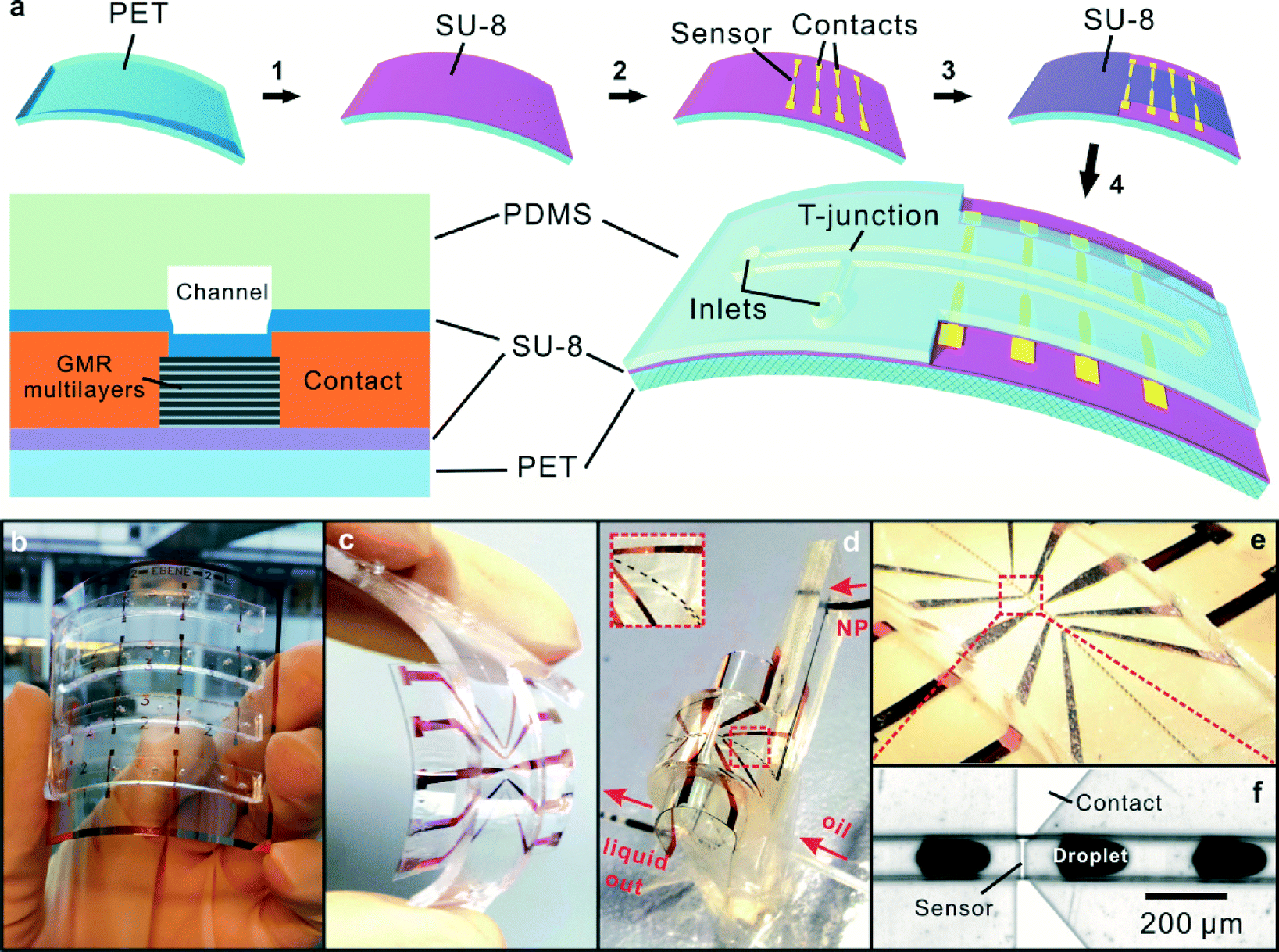 | ||
| Fig. 1 (a) Fabrication process of a flexible magnetoresistive analytic device, which is composed of several steps: (1) a layer of thin SU-8 polymer is spin-coated on a flexible PET foil; (2) GMR multilayers and electrical contacts are patterned on the SU-8-buffered PET foil; (3) a second thin SU-8 polymer is coated on top of sensors and contacts as an insulating layer; and (4) a PDMS-casted microfluidic channel is assembled with the bottom polymer-sandwiched GMR sensors. (Bottom left in panel) Schematic representation of the cross section of a flexible polymer-sandwiched microfluidic GMR device. (b) Photograph of a large area of electrodes integrated with microfluidic channels. (c) Photograph of a flexible GMR-based analytical device. (d) Photograph of a highly flexible GMR-based analytic device filled with liquid and producing emulsion droplets on chip. (Inset) Magnification of the part marked with a red rectangle on the chip. (e) The real-time detection of a train of emulsion droplets with encapsulated magnetic nanoparticles (f) which are passing across the sensor. | ||
As a first step, we used a flexible SU-8 polymeric material to buffer the GMR sensor as the commercially available PET foil used is characterized by a relatively pronounced roughness (~15 nm, root mean square), which can affect the interfacial-mediated GMR effect.50 Coating SU-8 on a PET foil flattens its surface substantially (Fig. S2†). Magnetoelectrical characterization of [Py/Cu]30 multilayers coupled at the 1st and the 2nd antiferromagnetic maximum deposited on different supports (PET foil, polymer-buffered PET foil and silicon substrate) is compared in Fig. S1.† The enhancement of the GMR ratio after polymer buffering is attributed to the enhancement of the interlayer exchange coupling strength at reduced roughness.50
To ensure the highest sensitivity, it is crucial to adjust the size of the GMR sensor to be compatible with the dimensions of the magnetic objects under investigation. A top-down approach was used to structure the GMR sensors into rectangular stripes with a constant width of 6 μm and different lengths of 20, 40, 60, and 100 μm (Fig. S5†). Detailed characterization of the structured GMR sensors reveals that the change in the sensor resistance scales with the aspect ratio of GMR sensors. Independent of the length, the performance of the sensors patterned on one substrate remains the same with a GMR ratio of about 14%. The variability of the sensitivity of these patterned sensors on one substrate is ±0.05% Oe−1. The GMR ratio is defined as the ratio of the change of sample resistance under external magnetic field Hext: GMR(Hext) = (R(Hext) − R(Hsat))/R(Hsat), where R(Hsat) is the sensor resistance when saturating magnetic field, Hsat, is applied.48 A GMR sensor (width 6 μm × length 100 μm, Fig. 2b, upper panel) was integrated into a microfluidic channel with a cross-sectional area of 100 × 100 μm2 (Fig. 2b, bottom panel). The magnetoelectrical characterization of the integrated sensor (Fig. 2a) confirms the excellent performance of the device with a GMR ratio of 14% and a maximum sensitivity of 0.4% Oe−1 at low field of 12 Oe. Here, the sensitivity is given by S(Hext) = [dR(Hext)/dHext]/R(Hsat).48 With the variability of the sensitivity of GMR sensors between substrates being within ±0.1% Oe−1, the performance of the polymer-buffered GMR sensor on a PET foil is higher than that of the sensor (0.26% Oe−1) previously demonstrated on a silicon substrate,41 which could be ascribed to the enhanced interlayer exchange coupling across GMR multilayers.50
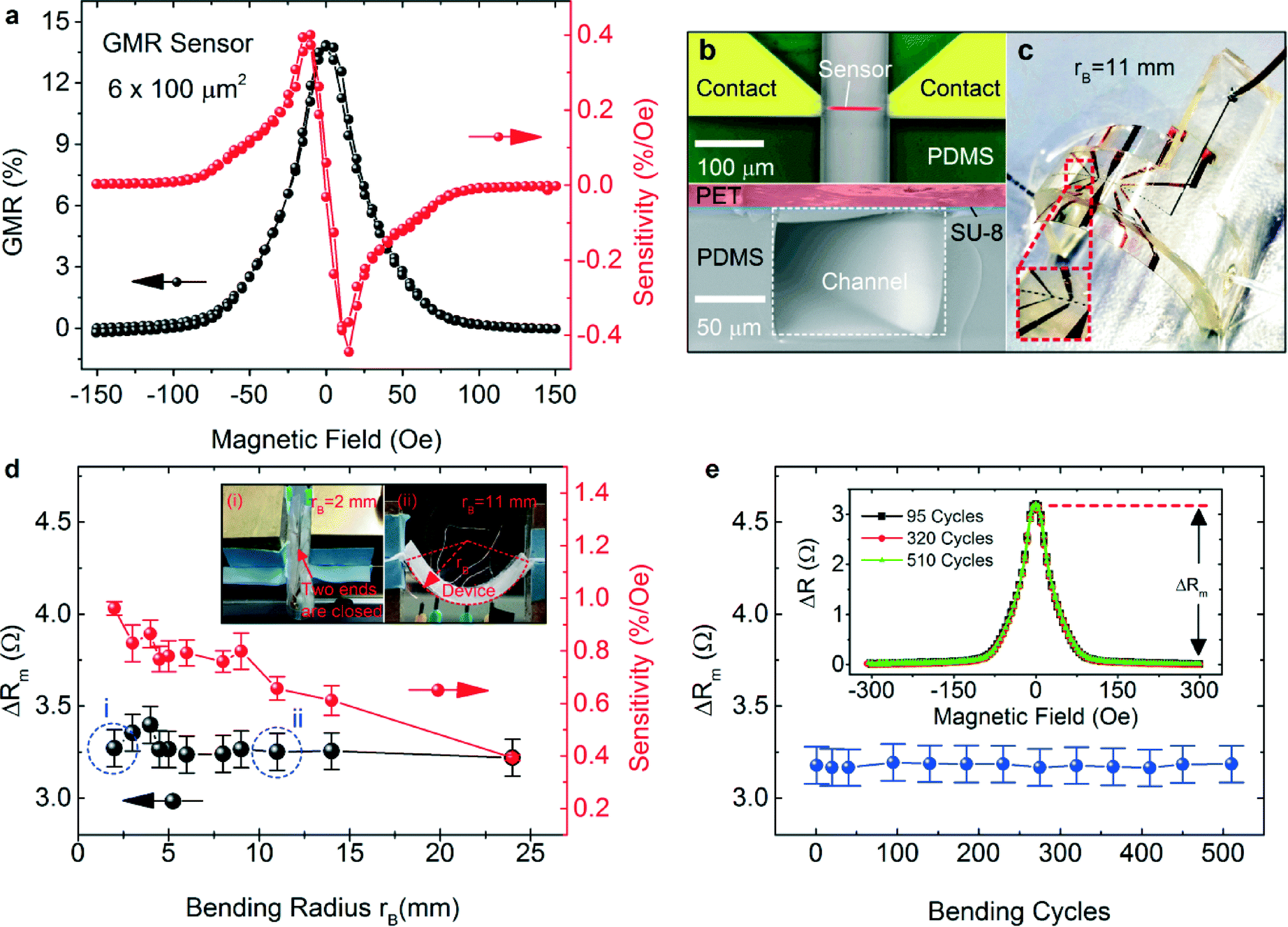 | ||
| Fig. 2 (a) GMR curve (black) and derived magnetic-field-dependent sensitivity (red) of a flexible GMR sensor stripe with a size of 6 × 100 μm2. (b) (Upper panel) Color-coded micrograph of a flexible GMR sensor stripe integrated into a PDMS microfluidic channel. (Bottom panel) SEM image of the cross section of the microfluidic channel cut by a pair of scissors. The channel has a height and width of 100 μm. (c) Photograph of the device filled with liquid and producing emulsion droplets with encapsulated magnetic nanoparticles (NPs) with a bending radius of 11 mm. The inset shows the magnification of the part marked with the red rectangle. The small black dots visible in the channel are the emulsion droplets as produced in the microfluidic channel. (d) Response of the GMR device at different bending states. The maximum change in the resistance (ΔRm, see the inset in (e)) of the GMR sensor was recorded for different bending radii. The maximum average sensitivity of the sensor is plotted against different bending radii (red). The insets show photographs of the device which is bent to a bending radius (rB) of 2 mm (i), when two ends of the device were closed, and 11 mm (ii). Error bars of the maximum sensitivity are standard deviations of the 4 sensitivity values derived during one cycle of magnetoelectrical characterization. (e) The maximum change in the sensor resistance during cyclic bending. For this experiment, the device was reversibly bent from the relaxed state to a radius of 8 mm. The inset shows the change in the sensor resistance for a magnetic field sweep after 95, 320, and 510 cycles of bending and unbending. Error bars for ΔRm in (d) and (e) are the precision of a multimeter (Keithley 2000) used for measuring the resistance. | ||
To ensure the operation of the GMR sensor in liquid environments, an appropriate electrical insulation is required. We went beyond the traditional insulating approach, i.e., covering with a layer of brittle oxides such as SiO2 and Al2O3.42 Instead, we adopted a strategy by encapsulating the sensor between two flexible polymer layers. As SU-8 is an epoxy-based polymer, the whole assembly process with the PDMS channel is facilitated by creating amine groups on the PDMS surface and harnessing the epoxy–amine reaction (details of the preparation are given in the methods section).53 The assembly process was carried out under liquid-free conditions since drying out the whole device was usually tedious and time-consuming. The final assembled device is shown in Fig. 1c. The fluidic functionality is demonstrated by its capability of delivering fluids and producing emulsion droplets on chip (Fig. 1d–f).
Mechanical performance of the device
The whole GMR device (integrated sensor size: 6 × 100 μm2) with an integrated microfluidic channel was mounted on a mechanical loading stage on which the device could be continuously bent, and corresponding magnetoelectrical characterization of the GMR sensor was simultaneously performed. Fig. 2d–e show the performance of the integrated GMR sensor during bending tests. The total thickness of the device including the PDMS channel is about 2.3 mm. We continuously bent the device until two of its ends were almost closed (Fig. 2d, inset i), revealing a minimum bending radius of about 2 mm, which is superior to conventional inorganic materials of 100 μm thickness that can only reach a bending limit of about 5 mm.51 The total electrical resistance (including the sensor and electrical contacts) was measured without applying an external magnetic field and at an external magnetic field of 300 Oe (Fig. S6d†) when the device was gradually bent to the minimum radius of 2 mm. The consistent behavior of the measured total resistance shows that the sensor was electrically well contacted during the entire bending cycle. A slight reduction in the saturation field of the sensor can be observed from the measurement of the resistance change under cyclic magnetic fields (Fig. S6c†) possibly due to the magnetostriction effect; however, the sensor is still functional without degrading the performance, which is reflected by the constant maximum change in sensor resistance Rm with the magnetic field during the magnetoelectrical characterization (Fig. 2d). For the magnetic detection, the reduction in the saturation field leads to the corresponding reduction in the sensing range for magnetic in-flow detection. However, the sensitivity of the sensor increases from about 0.4% Oe−1 to about 1% Oe−1 with increasing bending of the device.The robustness of the device against uninterrupted mechanical deformation was tested by reversibly bending the same device back and forth to a target radius of 8 mm. Remarkably, more than 500 cycles of bending were achieved with the device delivering full performance without any detachment of the microfluidic channel from the substrate. In addition, the sensor and electrical contacts did not show any degradation in performance in terms of the measured total resistance (Fig. S6e†) and the maximum change in the sensor resistance during magnetoelectrical characterization (Fig. 2e), which is reflected in the exact overlapping of the measured GMR curves summarizing the change in the sensor resistance with varying magnetic fields after different bending cycles (Fig. 2e, inset). One of the primary goals of fabricating an effective flexible microfluidic device is to demonstrate its capability of delivering liquids under various bending states. We connected the device to external supply tubes where hydrocarbon oil and aqueous magnetic nanoparticles can be injected via two separate inlets. Various bended states were realized by gradually closing the two ends of the device which were fixed on a stage (Fig. 2c and Fig. S7†). It is clearly visible that magnetic emulsion droplets can be produced well even when the device was bent to the minimum radius of 2 mm (Fig. 1d), thus demonstrating it to be the most flexible microfluidic device reported so far.
Analytic features of the device
To demonstrate the magnetic functionality of the device, superparamagnetic ferrofluid nanoparticles with a nominal particle size of 10 nm (Ferrotec, EMG 700) were encapsulated inside the emulsion droplets formed by a T-shaped on-chip junction (Fig. S4†). The emulsion droplets were pumped across the surface of an integrated GMR sensor one by one. As the ferrofluid magnetic nanoparticles are superparamagnetic, an external permanent magnet made of AlNiCo (A1045, IBSMagnet) was placed below the sensor to induce the net magnetic moment from the droplets and simultaneously bias the sensor to the most sensitive region (details are provided in the ESI†). The magnetic stray fields of the ferrofluid emulsion droplets were detected by the integrated GMR sensor, which is evidenced by characteristic detection events of the droplets consisting of isolated peaks of the voltage signal (Fig. 3a). The detection peak features its signal width and amplitude. As a GMR sensor is a proximity sensor, only local magnetic stray fields contribute to the final detected signal. Owing to this feature, the dimensions of an emulsion droplet containing magnetic nanoparticles can be derived from the detection peak width. Furthermore, as the amplitude of magnetic stray fields is proportional to the amount of magnetic nanoparticles in a droplet, the amplitude of the detection signal is related to the amount of magnetic content in the droplets, rendering the device an analytical tool.41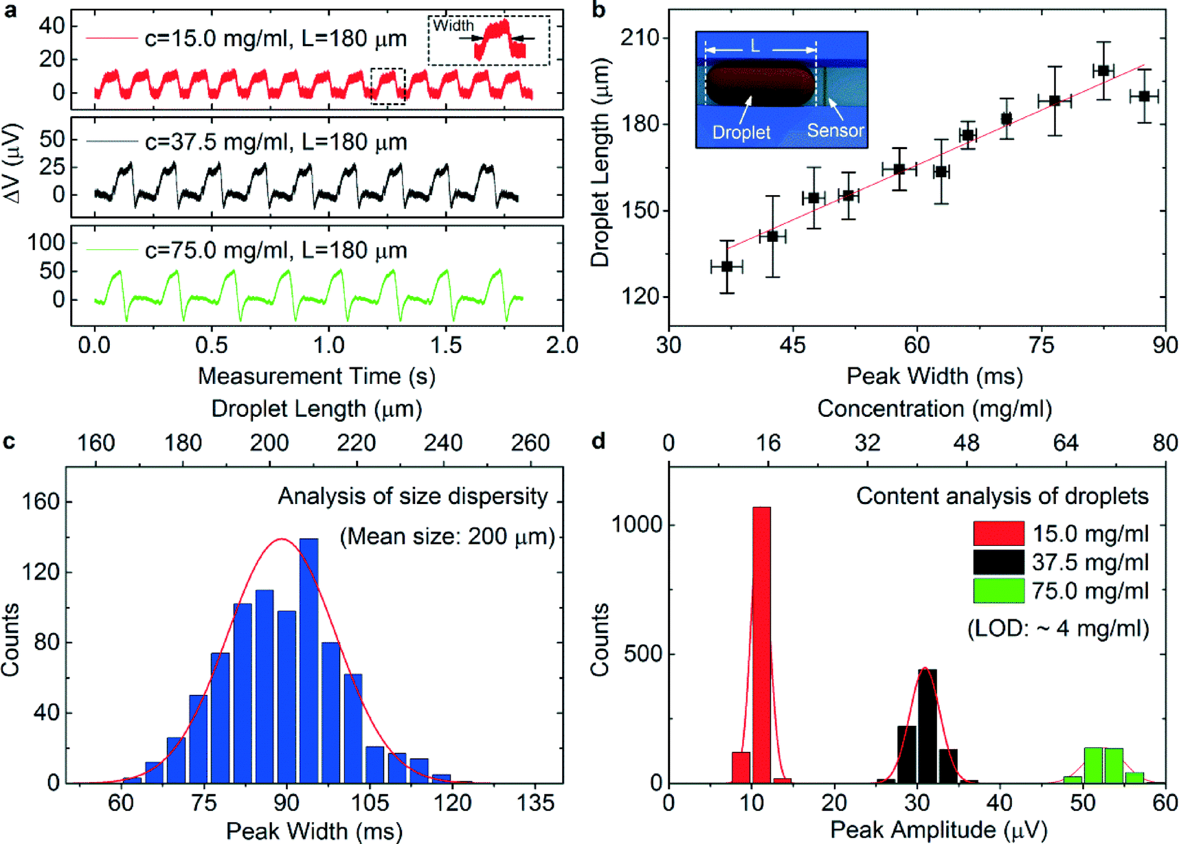 | ||
| Fig. 3 (a) Real-time in-flow detection of magnetic droplets with different concentrations, c, of encapsulated magnetic nanoparticles for a train of droplets with a size of 180 μm (within 2 s of measurement time). The voltage change (ΔV) of the device is recorded over time. (b) Dependence of the measured droplet length on the detection peak width for sequentially produced droplets of various sizes. The line represents a linear fit of the data. (Inset) Schematic sketch of a droplet in a microfluidic channel with the droplet length (denoted by L) measured along the travelling direction. (c) Histogram of the detection peak width for around 1000 emulsion droplets containing magnetic nanoparticles of 37.5 mg ml−1. The top x-axis denotes the corresponding droplet length. The red curve shows a Gaussian fit to the histogram. (d) Histograms of the detection peak amplitude for more than 1000 emulsion droplets with different concentrations of encapsulated magnetic nanoparticles (15.0 mg ml−1, 37.5 mg ml−1 and 75.0 mg ml−1). The top x-axis corresponds to the concentration of encapsulated magnetic nanoparticles. The curves show Gaussian fits to the respective histograms. | ||
The real-time in-flow detection of magnetic droplets with different concentrations of encapsulated magnetic nanoparticles is shown in Fig. 3a. The detection peak features a local maximum and a local minimum in the signal amplitude located at the rising and the falling edge, respectively, as local stray field maximum and minimum occur at the two ends of a magnetic droplet when it is magnetized by an external magnetic field.41Fig. 3a shows that the detection of emulsion droplets of the same size but loaded with higher concentrations of magnetic nanoparticles gives higher signal amplitudes (~55 μV for 75 mg ml−1, ~30 μV for 37.5 mg ml−1 and ~10 μV for 15.0 mg ml−1 of magnetic nanoparticles). We further produced a train of magnetic emulsion droplets of various sizes. As the detection peak width is independent of the concentration of magnetic nanoparticles in a droplet, it can be used to correlate the individual detection peak with each passing emulsion droplet.41 The real-time detection of these emulsion droplets is displayed in Fig. S8.†Fig. 3b plots the measured droplet size (denoted by L in the schematic sketch) against the detection peak width for the sequentially produced droplets. We observe clear linear dependence of the droplet size on the peak width. The coefficient (1.3 ± 0.1 mm s−1) between the droplet size and the peak width derived from a linear fit of the data agrees well with the flowing speed of the droplets (1.5 ± 0.1 mm s−1, determined by video analysis) in the microfluidic channel. The slight deviation from a perfect linear relationship is caused by the deviation in measuring the droplet length and the peak width, which is because of the limited resolution (10 μm) of the optical digital microscope (ISM-PM160L) and the slight deviation (±0.1 mm s−1) in the flow speed. The precision of the detection peak width (1 ms) obtained with the device is determined by electronic settings (sampling rate of 5 kHz), which reveals that the precision of determining the droplet size is about 1.5 μm under a constant flow speed of 1.5 mm s−1. Thus, the magnetic sensors provide very precise information on the size of emulsion droplets without the use of complex and bulky optical detection schemes,52 which is crucial for applications in wearable diagnostic electronics.
Furthermore, the device allows monitoring of the evolution of droplets under various flow mechanisms, i.e., distinguishing between squeezing and dripping regimes in microfluidics without the use of optical methods. We put forth a theoretical model (Fig. S9†) that allows correlating the reduction in the droplet volume to the decrease in the amplitude and width of detection peaks when the droplet is smaller than the channel dimensions. The minimum size of an emulsion droplet encapsulated with 37.5 mg of magnetic nanoparticles per milliliter that can be detected by the device is estimated to be 10 μm in diameter (~0.5 pl in volume) in a channel with a cross-sectional area of 100 × 100 μm2, which unveils the potential of the device in applications such as sensing magnetic objects encapsulated in an even much smaller volume, i.e., magnetically labeled biological cells for cytometry applications.
As the device is capable of resolving magnetic emulsion droplets in terms of size and magnetic content, it can find its application in analyzing the distribution of the droplet size and concentration of magnetic nanoparticles over large arrays. For example, histograms of the peak width (Fig. 3c) and amplitude (Fig. 3d) are used to statistically analyze the distribution of the size and concentrations of magnetic nanoparticles in a large scale of emulsion droplets, respectively. A Gaussian fit to the histogram reveals that the average size of around 1000 as-produced droplets is about 200 μm with a standard deviation of 12 μm, while Fig. 3d analyzes the magnetic content of more than 1000 droplets encapsulating different concentrations of loaded magnetic nanoparticles. We measured emulsion droplets of around 1 nl containing various concentrations of magnetic nanoparticles ranging from 15.0 mg ml−1 to 75 mg ml−1; the voltage signal on different concentrations of magnetic nanoparticles is shown in Fig. S10.† Linear interpolation of the data to the noise level of the device (~2.5 μV) reveals the limit of detection (LOD) of the device to be around 4 mg ml−1, enabling the device to be used as a quantification tool for the identification of the amount of magnetic materials used for on-chip manipulation of emulsion droplets encapsulated with other reagents.25
The current LOD of the device is set by several factors, i.e., the thickness of the insulation layer, the magnetic field configuration used for biasing the sensor and magnetizing nanoparticles as well as measurement electronics. A detailed comparison of the LOD of the present device with those of prior studies has been made in the ESI.† As shown, the LOD of the magnetic moment of a droplet for the present device is about 2 × 10⁻¹⁰ emu for a droplet of 0.5 pl, which is estimated for a microfluidic channel with a height of 100 μm. The LOD of our device is comparable with the previously reported value (2 × 10⁻¹⁰ emu) for devices integrated in a 10 μm high channel.55 Thus, a hydrodynamic focusing approach39 could be used to reduce the physical separation distance between the sensor and the targets to detect such small droplets (0.5 pl) or bacteria and pathogens with even smaller dimensions (~1 μm). Further, the thickness of the insulation layer (~700 nm) could be further reduced to enhance sensitivity as the signal level inversely scales with z3 (z being the distance of magnetic objects from the sensor surface). In addition, a relatively larger out-of-plane magnetic field (up to 190 mT) can be used to induce a larger magnetic moment of magnetic nanoparticles to magnetize without saturating the sensor.42
Conclusions
We developed a flexible microfluidic device equipped with in situ magnetic functionality. Compared with presently existing magnetic flow detectors fabricated on rigid substrates,40–44 the direct advantages our approach provides are the feasibility of cost-efficient production and prospect of mass production due to the low cost and light weight of flexible foils. The remarkable mechanical properties of the device compared with those of rigid counterparts, i.e., a minimum bending radius of 2 mm and over 500 cycles of bending, promise the long-term stability of the device for practical applications.Although the current device possesses merely magnetic functionality, it could be extended for future applications. An example can be made in the application of in vivo flow cytometry, which is performed directly in the human body. In such a case, magnetic nanoparticles have been used to enrich biomarkers to the near-skin area to enhance the detection which already combines optical and acoustical methods.54 Naturally, a magnetic functional element could be used for such an application to directly detect biomarkers labeled with magnetic particles. In order to have the best cooperation with the human body, a bendable device which can provide such magnetic functionality is anticipated. Our present device provides the state-of-the-art solution to incorporate magnetic elements on a flexible platform that could be potentially implemented in such a type of modern biomedical device by combining optical, magnetic, acoustical, and chemical sensitivities in order to realize modern multifunctional biomedical devices which are lightweight, wearable or even implantable.
Acknowledgements
The authors thank Dr. L. Baraban (TU Dresden) for fruitful discussions on magnetic cytometry, I. Fiering (IFW Dresden) for assistance in metal deposition, and B. Eichler (IFW Dresden) for AFM measurements. We acknowledge the financial support from the DFG Research Group 1713 and the European Research Council under the European Union's Seventh Framework Programme (FP7/2007-2013)/ERC grant agreement no. 306277.Notes and references
- D.-H. Kim, J.-H. Ahn, W. M. Choi, H.-S. Kim, T.-H. Kim, J. Song, Y. Y. Huang, Z. Liu, C. Lu and J. A. Rogers, Science, 2008, 320, 507 CrossRef CAS PubMed.
- J. A. Rogers, T. Someya and Y. Huang, Science, 2010, 327, 1603–1607 CrossRef CAS PubMed.
- H. Nishide and K. Oyaizu, Science, 2008, 319, 737–738 CrossRef CAS PubMed.
- N. Li, Z. Chen, W. Ren, F. Li and H.-M. Cheng, Proc. Natl. Acad. Sci. U. S. A., 2012, 109, 17360–17365 CrossRef CAS PubMed.
- M. S. White, M. Kaltenbrunner, E. D. Głowacki, K. Gutnichenko, G. Kettlgruber, I. Graz, S. Aazou, C. Ulbricht, D. A. M. Egbe, M. C. Miron, Z. Major, M. C. Scharber, T. Sekitani, T. Someya, S. Bauer and N. S. Sariciftci, Nat. Photonics, 2013, 7, 811–816 CrossRef CAS.
- S. S. P. Parkin, Appl. Phys. Lett., 1996, 69, 3092 CrossRef CAS PubMed.
- Y. Chen, Y. Mei, R. Kaltofen, J. I. Mönch, J. Schumann, J. Freudenberger, H.-J. Klauß and O. G. Schmidt, Adv. Mater., 2008, 20, 3224–3228 CrossRef CAS PubMed.
- M. Melzer, D. Makarov, A. Calvimontes, D. Karnaushenko, S. Baunack, R. Kaltofen, Y. Mei and O. G. Schmidt, Nano Lett., 2011, 11, 2522–2526 CrossRef CAS PubMed.
- G. H. Gelinck, H. E. A. Huitema, E. van Veenendaal, E. Cantatore, L. Schrijnemakers, J. B. P. H. van der Putten, T. C. T. Geuns, M. Beenhakkers, J. B. Giesbers, B.-H. Huisman, E. J. Meijer, E. M. Benito, F. J. Touwslager, A. W. Marsman, B. J. E. van Rens and D. M. de Leeuw, Nat. Mater., 2004, 3, 106–110 CrossRef CAS PubMed.
- Y. Chen, J. Au, P. Kazlas, A. Ritenour, H. Gates and M. McCreary, Nature, 2003, 423, 136 CrossRef CAS PubMed.
- M. Kaltenbrunner, T. Sekitani, J. Reeder, T. Yokota, K. Kuribara, T. Tokuhara, M. Drack, R. Schwödiauer, I. Graz, S. Bauer-Gogonea, S. Bauer and T. Someya, Nature, 2013, 499, 458–463 CrossRef CAS PubMed.
- G. A. Salvatore, N. Münzenrieder, T. Kinkeldei, L. Petti, C. Zysset, I. Strebel, L. Büthe and G. Tröster, Nat. Commun., 2014, 5, 2982 Search PubMed.
- M. Kaltenbrunner, M. S. White, E. D. Głowacki, T. Sekitani, T. Someya, N. S. Sariciftci and S. Bauer, Nat. Commun., 2012, 3, 770 CrossRef PubMed.
- F. Eder, H. Klauk, M. Halik, U. Zschieschang, G. Schmid and C. Dehm, Appl. Phys. Lett., 2004, 84, 2673 CrossRef CAS PubMed.
- W. Dungchai, O. Chailapakul and C. S. Henry, Anal. Chem., 2009, 81, 5821–5826 CrossRef CAS PubMed.
- Z. Nie, C. A. Nijhuis, J. Gong, X. Chen, A. Kumachev, A. W. Martinez, M. Narovlyansky and G. M. Whitesides, Lab Chip, 2010, 10, 477–483 RSC.
- N. Godino, R. Gorkin, K. Bourke and J. Ducrée, Lab Chip, 2012, 12, 3281–3284 RSC.
- F. Vatansever, R. Burtovyy, B. Zdyrko, K. Ramaratnam, T. Andrukh, S. Minko, J. R. Owens, K. G. Kornev and I. Luzinov, ACS Appl. Mater. Interfaces, 2012, 4, 4541–4548 CAS.
- S. Metz, A. Bertsch, D. Bertrand and P. Renaud, Biosens. Bioelectron., 2004, 19, 1309–1318 CrossRef CAS PubMed.
- E. I. Galanzha, E. V. Shashkov, T. Kelly, J.-W. Kim, L. Yang and V. P. Zharov, Nat. Nanotechnol., 2009, 4, 855–860 CrossRef CAS PubMed.
- L. C. Branquinho, M. S. Carrião, A. S. Costa, N. Zufelato, M. H. Sousa, R. Miotto, R. Ivkov and A. F. Bakuzis, Sci. Rep., 2013, 3, 2887 Search PubMed.
- S. J. Osterfeld, H. Yu, R. S. Gaster, S. Caramuta, L. Xu, S.-J. Han, D. A. Hall, R. J. Wilson, S. Sun, R. L. White, R. W. Davis, N. Pourmand and S. X. Wang, Proc. Natl. Acad. Sci. U. S. A., 2008, 105, 20637–20640 CrossRef CAS PubMed.
- L. A. Sasso, I. H. Johnston, M. Zheng, R. K. Gupte, A. Ündar and J. D. Zahn, Microfluid. Nanofluid., 2012, 13, 603–612 CrossRef CAS.
- R. S. Gaster, D. A. Hall and S. X. Wang, Lab Chip, 2011, 11, 950–956 RSC.
- J. S. Sander, R. M. Erb, C. Denier and A. R. Studart, Adv. Mater., 2012, 24, 2582–2587 CrossRef CAS PubMed.
- Y. Zhang and T.-H. Wang, Adv. Mater., 2013, 25, 2903–2908 CrossRef CAS PubMed.
- R. S. Gaster, D. A. Hall, C. H. Nielsen, S. J. Osterfeld, H. Yu, K. E. Mach, R. J. Wilson, B. Murmann, J. C. Liao, S. S. Gambhir and S. X. Wang, Nat. Med., 2009, 15, 1327–1332 CrossRef CAS PubMed.
- V. C. Martins, F. A. Cardoso, J. Germano, S. Cardoso, L. Sousa, M. Piedade, P. P. Freitas and L. P. Fonseca, Biosens. Bioelectron., 2009, 24, 2690–2695 CrossRef CAS PubMed.
- G. Reiss, H. Brueckl, A. Huetten, J. Schotter, M. Brzeska, M. Panhorst, D. Sudfeld, A. Becker, P. B. Kamp, A. Puehler, K. Wojczykowski and P. Jutzi, J. Mater. Res., 2011, 20, 3294–3302 CrossRef.
- J. C. Rife, M. M. Miller, P. E. Sheehan, C. R. Tamanaha, M. Tondra and L. J. Whitman, Sens. Actuators, A, 2003, 107, 209–218 CrossRef CAS.
- X. Zhi, Q. Liu, X. Zhang, Y. Zhang, J. Feng and D. Cui, Lab Chip, 2012, 12, 741–745 RSC.
- X. Zhi, M. Deng, H. Yang, G. Gao, K. Wang, H. Fu, Y. Zhang, D. Chen and D. Cui, Biosens. Bioelectron., 2014, 54, 372–377 CrossRef CAS PubMed.
- R. L. Millen, J. Nordling, H. A. Bullen, M. D. Porter, M. Tondra and M. C. Granger, Anal. Chem., 2008, 80, 7940–7946 CrossRef CAS PubMed.
- R. L. Millen, T. Kawaguchi, M. C. Granger, M. D. Porter and M. Tondra, Anal. Chem., 2005, 77, 6581–6587 CrossRef CAS PubMed.
- W. Shen, B. D. Schrag, M. J. Carter and G. Xiao, Appl. Phys. Lett., 2008, 93, 33903 CrossRef PubMed.
- F. A. Cardoso, J. Germano, R. Ferreira, S. Cardoso, V. C. Martins, P. P. Freitas, M. S. Piedade and L. Sousa, J. Appl. Phys., 2008, 103, 07A310 Search PubMed.
- S. Gambini, K. Skucha, P. P. Liu, J. Kim and R. Krigel, IEEE J. Solid-State Circuits, 2013, 48, 302–317 CrossRef.
- D. Issadore, J. Chung, H. Shao, M. Liong, A. A. Ghazani, C. M. Castro, R. Weissleder and H. Lee, Sci. Transl. Med., 2012, 4, 141ra92 Search PubMed.
- D. Issadore, H. J. Chung, J. Chung, G. Budin, R. Weissleder and H. Lee, Adv. Healthcare Mater., 2013, 2, 1224–1228 CrossRef CAS PubMed.
- I. Mönch, D. Makarov, R. Koseva, L. Baraban, D. Karnaushenko, C. Kaiser, K.-F. Arndt and O. G. Schmidt, ACS Nano, 2011, 5, 7436–7442 CrossRef PubMed.
- G. Lin, L. Baraban, L. Han, D. Karnaushenko, D. Makarov, G. Cuniberti and O. G. Schmidt, Sci. Rep., 2013, 3, 2548 Search PubMed.
- J. Loureiro, P. Z. Andrade, S. Cardoso, C. L. da Silva, J. M. Cabral and P. P. Freitas, Lab Chip, 2011, 11, 2255–2261 RSC.
- K. Aledealat, G. Mihajlovic, K. Chen, M. Field, G. J. Sullivan, P. Xiong, P. B. Chase and S. von Molnar, J. Magn. Magn. Mater., 2010, 322, L69–L72 CrossRef CAS PubMed.
- N. Pekas, M. D. Porter, M. Tondra, A. Popple and A. Jander, Appl. Phys. Lett., 2004, 85, 4783 CrossRef CAS PubMed.
- C.-H. Chen, A. R. Abate, D. Lee, E. M. Terentjev and D. A. Weitz, Adv. Mater., 2009, 21, 3201–3204 CrossRef CAS PubMed.
- M. Tondra, M. Porter and R. J. Lipert, J. Vac. Sci. Technol., A, 2000, 18, 1125–1129 CAS.
- S. S. P. Parkin, K. P. Roche and T. Suzuki, Jpn. J. Appl. Phys., 1992, 31, L1246–L1249 CrossRef CAS.
- M. Melzer, D. Karnaushenko, D. Makarov, L. Baraban, A. Calvimontes, I. Mönch, R. Kaltofen, Y. Mei and O. G. Schmidt, RSC Adv., 2012, 2, 2284 RSC.
- M. Melzer, G. Lin, D. Makarov and O. G. Schmidt, Adv. Mater., 2012, 24, 6468–6472 CrossRef CAS PubMed.
- Y. Chen, Y. Mei, A. Malachias, J. Ingolf Mönch, R. Kaltofen and O. G. Schmidt, J. Phys.: Condens. Matter, 2008, 20, 452202 CrossRef.
- T. Someya, Stretchable electronics, John Wiley & Sons, 2012 Search PubMed.
- L. Baraban, F. Bertholle, M. L. M. Salverda, N. Bremond, P. Panizza, J. Baudry, J. A. G. M. de Visser and J. Bibette, Lab Chip, 2011, 11, 4057–4062 RSC.
- Z. Zhang, P. Zhao, G. Xiao, B. R. Watts and C. Xu, Biomicrofluidics, 2011, 5, 46503–465038 CrossRef PubMed.
- E. I. Galanzha, E. V. Shashkov, T. Kelly, J.-W. Kim, L. Yang and V. P. Zharov, Nat. Nanotechnol., 2009, 4, 855–860 CrossRef CAS PubMed.
- I. Jeong, et al. , J. Magn. Soc. Jpn., 2012, 17(4), 302 Search PubMed.
- A. Bedoya-Pinto, M. Donolato, M. Gobbi, L. E. Hueso and P. Vavassori, Appl. Phys. Lett., 2014, 104, 062412 CrossRef PubMed.
- M. Melzer, A. Kopylov, D. Makarov and O. G. Schmidt, SPIN, 2013, 03, 1340005 CrossRef.
Footnote |
| † Electronic supplementary information (ESI) available. See DOI: 10.1039/c4lc00751d |
| This journal is © The Royal Society of Chemistry 2014 |