 Open Access Article
 This Open Access Article is licensed under a
 Creative Commons Attribution 3.0 Unported Licence
Atomic layer deposition of ferroelectric LiNbO3†
Erik
Østreng
*a,
Henrik H.
Sønsteby
a,
Timo
Sajavaara
b,
Ola
Nilsen
a and
Helmer
Fjellvåg
a
aCentre for Materials Science and Nanotechnology, Department of Chemistry, University of Oslo, P.O. Box 1033 Blindern, N-0315 Oslo, Norway. E-mail: erik.ostreng@smn.uio.no; Fax: +47 2285 5565; Tel: +47 2285 5558
bDept of Physics, University of Jyväskylä, FIN-40014, Finland
First published on 13th May 2013
Abstract
The ferroelectric and electro-optical properties of LiNbO3 make it an important material for current and future applications. It has also been suggested as a possible lead-free replacement for present PZT-devices. The atomic layer deposition (ALD) technique offers controlled deposition of films at an industrial scale and thus becomes an interesting tool for growth of LiNbO3. We here report on ALD deposition of LiNbO3 using lithium silylamide and niobium ethoxide as precursors, thereby providing good control of cation stoichiometry and films with low impurity levels of silicon. The deposited films are shown to be ferroelectric and their crystalline orientations can be guided by the choice of substrate. The films are polycrystalline on Si (100) as well as epitaxially oriented on substrates of Al2O3 (012), Al2O3 (001), and LaAlO3 (012). The coercive field of samples deposited on Si (100) was found to be ∼220 kV cm−1, with a remanent polarization of ∼0.4 μC cm−2. Deposition of lithium containing materials is traditionally challenging by ALD, and critical issues with such deposition are discussed.
Introduction
Lithium niobate, LiNbO3, has been the centre of attention for a range of optical applications since the discovery of its ferroelectric properties in 1949.1 The non-centrosymmetric trigonal structure of LiNbO3 was described in detail by Nassau in 1966.2 The strength of LiNbO3 is its relatively large physical coefficients for piezoelectric,3 pyroelectric4 and photoelastic5 effects. Combinations of these effects have resulted in a range of technologically important applications, including acoustic wave transducers,6 optical modulators,7 Q-switches,8,9 optical waveguides10,11 and holographic memory modules.12,13 The ferroelectric response of LiNbO3 has previously gathered much attention, as the theoretical intrinsic coercive fields are as high as 5420 kV cm−1. The response is attributed to the lack of inversion symmetry in the trigonal cell (SG: R3c), and is oriented along the c-axis. However, due to polarization gradients at 180° domain walls, reported experimental values vary from 40 kV cm−1 for near stoichiometric to 210 kV cm−1 for congruent composition.14The area of ferroelectric thin films emerged in 1969 with deposition of Pb0.92Bi0.07La0.01(Fe0.405Nb0.325Zr0.27)O3 by Chapman,15 as a response to the need for non-volatile integrated memory devices. A range of applications have evolved over the last decades, and include microsensors,16 tuneable microwave applications17 and ferroresistive microelectronics.18
Undesired non-linear piezoresponse may occur in ferroelectric thin films due to domain-wall displacement. The effect has been shown to be mainly extrinsic due to manufacturing faults.19 This underlines the importance of synthesis of high quality ferroelectric thin films.
Ferroelectric Pb(Zr,Ti)O3 (PZT) has been the main material of choice for many applications owing to the high ferroelectric response and accessible synthetic routes. On the other hand, devices utilizing PZT, in particular when present as a nano-material, will be phased out owing to the toxicity of lead.20 LiNbO3 (LNO) is a possible lead-free replacement as values for the coercive field and the remanent polarization are comparable. Thin films of LiNbO3 have previously been deposited by numerous techniques, such as laser ablation,21pulsed laser deposition,22 molecular beam epitaxy23 and sol–gel routes,23 and now by atomic layer deposition (ALD). Atomic layer deposition is a proven thin film deposition technique that allows deposition of films on an industrial scale. ALD is also superior to other thin film deposition techniques with respect to uniformity and pinhole density, the latter is important for applications of ferroelectrics. An additional advantage of ALD is that it allows deposition of films on high aspect ratio structures, opening up possibilities for novel devices.
Deposition of lithium containing compounds by ALD has recently received notable attention.24–30Lithium phosphate and lithium silicate have been grown using lithium silylamide (LiN(SiMe3)2 or LiHMDS) as a precursor by Hämäläinen et al.26,28 and we have recently reported the growth of lithium nitride and carbonate by the same precursor.30 Alternative types of precursors reported for deposition of lithium compounds are Li(thd)27 (thd = 2,2,6,6-tetramethyl-3,5-heptadionate) and lithium tert-butoxide.24,25 The main focus for deposition of lithium compounds by ALD has so far been towards lithium ion battery applications.
Ferroelectric lead based oxides have previously been deposited by ALD by Harjuoja et al.31,32 while the deposition of bismuth titanates by ALD is reported by Vehkamäki etal.33 In addition, the growth of ferroelectric yttrium doped hafnium oxide by ALD has recently been reported.34 The current paper describes the epitaxial growth of ferroelectric LiNbO3 by atomic layer deposition (ALD). The remanent polarization has been measured to be ∼0.4 μC cm−2 and the coercive field is approximately 220 kV cm−1.
Experimental
Thin films were deposited in an ASM F-120 Sat ALD reactor (ASM Microchemistry Ltd) using lithium silylamide [LiN(SiMe3)2, Me = –CH3, hereafter termed LiHMDS], niobium ethoxide [Nb(OEt)5, Et = –CH2CH3] and deionized water as precursors. LiHMDS was sublimed in an open boat at 75 °C and the niobium precursor was kept at 100 °C. All deposition processes were performed with a substrate temperature of 235 °C. Nitrogen was used as the carrier gas supplied at a total rate of 500 cm3 min−1 from a Schmidelin-Sirocco-5 N2 generator providing >99.999% (N2 + Ar).All LiNbO3 films were deposited on soda lime glass as well as on silicon (100) wafers with native oxide. Selected deposition processes were made on single crystals of Al2O3 (001), Al2O3 (012), SrTiO3 (100) and LaAlO3 (012). In order to maintain reproducible deposition, the chamber was passivated between each run with Nb2O5 by supplying 2000 cycles of Nb(OEt)5 and water.
X-ray diffraction analysis was performed using a Bruker AXS D8 Discover powder diffractometer and a Bruker AXS D8 Advance thin film diffractometer, both equipped with a LynxEye strip detector. The powder diffractometer has a Ge(111) focusing monochromator providing CuKα1-radiation. The thin film diffractometer was equipped with a Göbel mirror and a Ge(220) four bounce monochromator for X-ray reflectivity (XRR) measurements and reciprocal space maps of symmetric reflections, whereas only a Göbel mirror was used for reciprocal space maps of asymmetric reflections. X-ray reflectivity data were analysed using the GenX software.35
A J. A.Woolam α-SE spectroscopic ellipsometer was used to determine the thickness and refractive index from data measured in the range 380–900 nm. The films were assumed transparent and the data were fitted using a Cauchy-model.
Time of flight elastic recoil detection analysis (TOF-ERDA) measurements were performed at the University of Jyväskylä using a 8.515 MeV 35Cl4+ beam from the 1.7 MV Pelletron accelerator. With this technique all the sample elements, including impurities above 0.1 at% concentration could be quantified. The only exception is Si, which was partly shadowed by the strong signal of 35Cl scattered from Nb. Scanning probe microscopy measurements were performed using a Park Systems XE-70 unit. Atomic force microscopy (AFM) measurements were performed in contact mode using a CONTSCR tip while the piezoresponse force microscopy (PFM) measurements were performed using a PPP-NCSTAu 3M gold plated silicon tip (Nanosensors) and an external lock-in amplifier (Standford Research Systems).
Measurements of ferroelectric properties are made with an Aixact TF2000 analyzer at 1 kHz.
Results
The growth of LiNbO3 was studied at the deposition temperature of 235 °C using 1 s pulse and purge parameters for all precursors. For deposition of Nb2O5, these parameters gave a growth rate of 0.46 Å per cycle compared to that of about 0.3 Å per cycle which is reported by Kukli et al.36 The growth rate was also verified through deposition in another reactor (Beneq TFS500) with the same result. The process has proven to be reproducible and shows self-limiting growth. We have adopted the same parameters for deposition of the lithium component as earlier reported for the same lithium precursor and deposition system.30A series of samples were made by varying the lithium to niobium pulsing ratio. The total number of cycles was kept close to 2000, whereas the composition and number of the sub-cycles were varied from no lithium and up to a 1![[thin space (1/6-em)]](https://www.rsc.org/images/entities/char_2009.gif) :1 pulsing ratio, see Table 1. For a 1:1 pulsing ratio of lithium to niobium, the deposition resulted in large, flame-like gradients and powder formation at the edges of the reaction chamber. It was therefore concluded that higher lithium pulsing ratios would lead to uncontrolled growth. The elemental composition was determined using TOF-ERDA, see Fig. 1 and 2. The data show the increasing lithium content with the number of lithium sub-cycles, as expected. The main impurities are sodium, carbon and hydrogen. Sodium impurities were found to be up to 3.5 at%, carbon was below 0.2 at% in most cases, except for the most lithium rich sample. The amount of hydrogen appears correlated with the lithium content and exists probably as lithium hydroxide in the film. Most importantly, there is no significant amount of silicon stemming from the precursor. This proves that the cleavage of the lithium nitrogen bond in the precursor is dominant and that the precursor does not incorporate silicon in the film, consistent with what is previously reported.30
:1 pulsing ratio, see Table 1. For a 1:1 pulsing ratio of lithium to niobium, the deposition resulted in large, flame-like gradients and powder formation at the edges of the reaction chamber. It was therefore concluded that higher lithium pulsing ratios would lead to uncontrolled growth. The elemental composition was determined using TOF-ERDA, see Fig. 1 and 2. The data show the increasing lithium content with the number of lithium sub-cycles, as expected. The main impurities are sodium, carbon and hydrogen. Sodium impurities were found to be up to 3.5 at%, carbon was below 0.2 at% in most cases, except for the most lithium rich sample. The amount of hydrogen appears correlated with the lithium content and exists probably as lithium hydroxide in the film. Most importantly, there is no significant amount of silicon stemming from the precursor. This proves that the cleavage of the lithium nitrogen bond in the precursor is dominant and that the precursor does not incorporate silicon in the film, consistent with what is previously reported.30
| Li pulses per sub-cycle | Average Nb pulses per sub-cycle | Pulsed ratio Li/(Li + Nb) (%) | Deposited ratio Li/(Li + Nb) (%) | Thickness (nm) | Refractive index at 632.8 nm |
|---|---|---|---|---|---|
| 0 | 1 | 0 | 0 | 92 ± 0.7 | 2.360 |
| 1 | 9 | 10 | 19.2 ± 3.2 | 82.9 ± 0.2 | 2.282 |
| 1 | 5 | 16.67 | 24.3 ± 4.5 | 90.3 ± 0.05 | 2.199 |
| 1 | 4 | 20 | 30.3 ± 6.1 | 81.5 ± 0.9 | 2.169 |
| 1 | 3 | 25 | 31.3 ± 6.2 | 89.5 ± 3.2 | 2.111 |
| 1 | 2.75 | 26.7 | 26.1 ± 4.3 | 121 ± 11.6 | 2.2 |
| 1 | 2 | 33 | 41.7 ± 5.5 | 128 ± 9 | 2.073 |
| 1 | 1 | 50 | 73.5 ± 5.8 | 191.5 ± 9 | 1.85 |
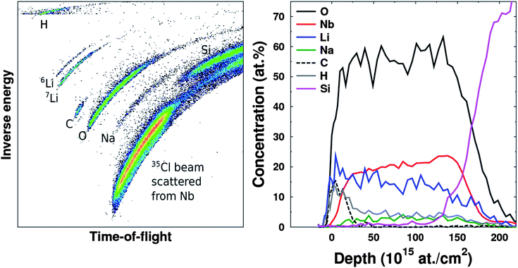 | ||
| Fig. 1 A raw time-of-flight-energy histogram from a TOF-ERDA measurement (left) and the corresponding elemental depth profiles (right) of a sample deposited on a Si substrate using 666 cycles of 2:1 Nb to Li pulsing ratio. | ||
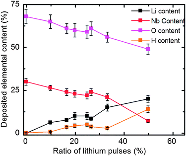 | ||
| Fig. 2 Element content in films deposited for different lithium pulsing ratios. | ||
The depth profiles achieved by TOF-ERDA clearly show a carbon and hydrogen enriched layer on top of all the deposited films. This is also supported by XRR-measurement data (see ESI†). The lithium content is also higher on the surface, indicating that lithium diffuses through the pristine films at room temperature. Even though there is evidence of formation of carbonate on the surface, the samples appeared stable in the duration of the study, except the sample with the highest lithium content which turned opaque over a few days in air.
The thickness and refractive index of the deposited films were derived from ellipsometry measurements. Both parameters correlate with the amount of pulsed lithium. There is a strong non-linear increase in thickness at high lithium pulsing ratios, probably due to the formation of lithium hydroxide which interferes with the self-limiting growth mechanism. This is also manifested in terms of increased non-uniformity for lithium rich samples. The refractive index varies quite linearly with the pulsed content of lithium, as shown in Fig. 3 and functions as a simple measure of the composition. However, high hydrogen concentrations will also contribute to a reduction in the refractive index. Hence, as long as the water dose is fairly constant, this simple approach appears as a reliable tool.
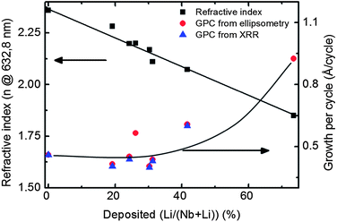 | ||
| Fig. 3 Refractive index and growth per cycle for LiNbO3 deposited using different ratios of lithium and niobium precursors. | ||
Thickness, roughness and density information were derived from X-ray reflectometry data. It became necessary to apply a four-layer model, consisting of the substrate, native oxide of SiO2, the LiNbO3-film and a surface carbonate layer, in order to properly fit the data. The density and composition of the carbonate layer are consistent with Li2CO3. The layer is probably amorphous as it cannot be identified by diffraction experiments. The thickness of this carbonate layer increases with the amount of lithium in the film from about 5 Å at low lithium contents to about 35 Å at high contents. As expected, there is a strong correlation between lithium content and film density. The films with 73.5 and 31.3% lithium were too rough or not uniform enough to measure.
Samples of different compositions were annealed at 650 °C for 5 min in air to trigger crystallization; the annealing conditions were based on preliminary results from another study to be reported later. The corresponding diffraction patterns in Fig. 4 show that the LiNbO3 phase is present in all samples with a lithium to niobium pulsing ratio higher than 16%. The films deposited using 33% lithium pulses appear as phase pure according to XRD. For all cases, the samples are polycrystalline showing some preferred orientation for selected samples. For higher lithium contents, the samples remain amorphous even after annealing. The samples deposited using 33% lithium pulses (i.e. 666 cycles of 2Nb + 1Li) appear phase pure, although the composition as measured by TOF-ERDA is 42 ± 5.5% lithium to niobium. The excess niobium must be present as an amorphous niobium rich phase considering that the solid solubility of niobium oxide in LiNbO3 is very low.37
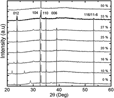 | ||
| Fig. 4 Powder X-ray diffractogram of samples with different pulsed compositions (Li pulsed content given in %) as deposited on silicon and annealed for 5 min at 650 °C. The vertical lines show positions for reflections from the LiNbO3-phase, the peak marked with * is Si (200) and the other peaks are from Nb2O5. | ||
A series of films based on 33% Li pulses were deposited on single crystal substrates and subsequently annealed in air at 650 °C for 15 min. The films were crystallized with different orientations depending on the substrates. Deposition on Al2O3 (001) leads to (001) oriented LiNbO3 whereas predominantly (012) oriented films were obtained on LaAlO3 (012) and Al2O3 (012), as shown in Fig. 5 and 6. Deposition on SrTiO3 (001) resulted in a mixture of (012) and (001) oriented crystallites. It is surprising that the film does not orient well on SrTiO3 as it is known that LaAlO3, which is different from LiNbO3 only by an inversion centre, grows epitaxially oriented as SrTiO3 (100)|SrTiO3[100]||LaAlO3 (012)|LaAlO3[100] when deposited with ALD.38 A more detailed reciprocal space mapping was then performed on the Al2O3 and LaAlO3 substrates which revealed quite large in-plane peak broadening compared to the out-of-plane broadening, see Fig. 5. Rocking curve analysis showed that c-Al2O3, r-Al2O3 and LaAlO3 had peak broadening of the first symmetric reflection (006 or 012) of 1.05°, 2.04° and 1.76°, respectively. In order to reveal the full epitaxial relationship on the different substrates reciprocal space maps and ϕ-scans were performed.
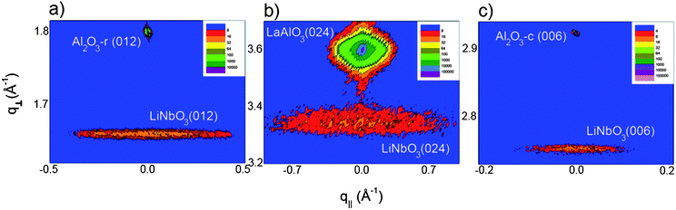 | ||
| Fig. 5 Reciprocal space maps of symmetric reflections for (a) LiNbO3 (012) on r-cut sapphire, (b) LiNbO3 (024) on LAO and (c) LiNbO3 (006) on c-cut sapphire. All show the proof of ordering identical to the substrate cut. The relatively large broadening in q|| is attributed to a small random tilt of the normal axis. Note, however, the very delimited tilt along the symmetric axis. | ||
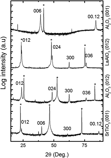 | ||
| Fig. 6 X-ray diffractogram collected in θ–2θ mode of a film deposited using 666 super-cycles consisting of two cycles of Nb(OEt)5 and H2O and one cycle of LiN(SiMe3)2 and H2O, thereafter annealed for 15 min at 650 °C. The substrates were Al2O3 (001), LaAlO3 (012), Al2O3 (012) and SrTiO3 (001). The substrate peaks are labelled with *. | ||
ϕ-Scans were performed on the (10.10)-reflection of the sample deposited on c-Al2O3 or the (122)-reflection of LaAlO3 or r-Al2O3 and the ϕ-scans revealed a perfect epitaxial relationship as shown in Fig. 8 and the ESI.† It was difficult to obtain reciprocal space maps of asymmetric reflections suitable for determination of the epitaxial relationship between the substrate and the film, both considering the intensity and geometrical constraints. An asymmetric reflex, (122), for r-cut Al2O3 (normal axis: (012)) was collected, showing the delimited intensity at the expected q-values for LiNbO3 (122), Fig. 7.
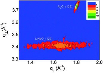 | ||
| Fig. 7 Reciprocal space map of the asymmetric (122)-reflection in the Al2O3 r-cut||LNO-system. The delimited intensity points towards an in-plane ordering in addition to the already described normal ordering. | ||
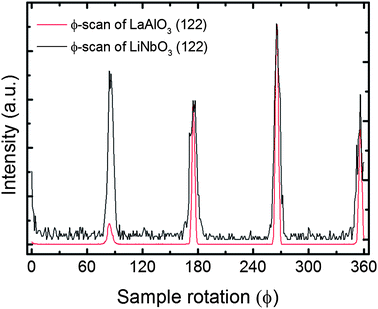 | ||
| Fig. 8 ϕ-Scan of the (122)-reflection for a film deposited on LaAlO3, proving the epitaxial relationship described. | ||
The observed ordering both in-plane and normal to the film, as measured on the r-cut sapphire substrate, points towards a strict epitaxial relationship on annealed substrate||film-systems, represented by Al2O3 (012)|Al2O3[100]||LiNbO3 (012)|LiNbO3[100]. An equivalent relationship is also shown for films deposited on LaAlO3.
For c-Al2O3 the relationship is Al2O3 (001)|Al2O3[100]||LiNbO3 (001)|LiNbO3[100] where the polar c-axis is oriented normal to the film. The surface morphology was characterised by AFM, see representative sample regions for different substrates in Fig. 9 and consists of crystallites with 200–300 nm diameter, separated by grain boundaries with precipitates of smaller crystallites. The crystallite size normal to the surface is estimated to be 44 ± 10 nm using a simplified Williamson–Hall approach based on the FWHM broadening of symmetric diffraction peaks of epitaxial films. The deviation in the TOF-ERDA compositional ratio of 1:1 for the lithium to niobium content, see above, indicates that the precipitates along the grain boundaries represent a nano-crystalline or amorphous niobium rich phase, possibly LiNb3O8 or niobium pentoxide. The RMS-roughness of the LiNbO3 films deposited on silicon, Al2O3 (001), Al2O3 (012), and LaAlO3 (012) are 1.6, 1.3, 1.3, and 1.8 nm, respectively. The roughness of the individual LiNbO3 facet surfaces is in the order of 0.1 nm.
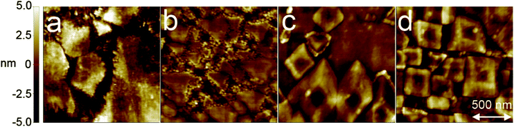 | ||
| Fig. 9 AFM images of films deposited on (a) Si (100), (b) Al2O3 (001), (c) Al2O3 (012) and (d) LaAlO3 (012) using 666 super-cycles each consisting of two cycles of Nb(OEt)5 and H2O and one cycle of LiN(SiMe3)2 and H2O, thereafter annealed for 15 min at 650 °C. | ||
The diffraction patterns in Fig. 6 suggest that the films deposited on different substrates should yield different morphologies as the exposed crystal facets are different. AFM images collected of the different samples show that this is indeed the case, as shown in Fig. 9. The sample deposited on Si (100) shows large grains with almost atomically flat plateaus, but no apparent crystal facets. However, the epitaxially oriented films show clearly crystallite shapes. On Al2O3 (001) the dominant crystallite shapes are triangular, reflecting the three-fold rotation axis normal to the surface. Furthermore, on Al2O3 (012) and LaAlO3 (012), the crystallites take octahedral morphology with flat tops, reflecting the symmetry in the (012) plane of the Al2O3, LiNbO3, and LaAlO3 crystal structures.
The piezoelectric response of a LiNbO3 thin film on silicon was studied using a PFM-setup where an external alternating current bias is applied to the tip. The piezoelectric response from the ferroelectric thin film created a modulated deflection of the PFM-tip, which was extracted using an external lock-in amplifier. In Fig. 10 such responses are clearly observable as separate regions with an 180° phase deviation that reflects the relative alignment of the polar axis. The sizes of the domains are similar to those of the crystalline grains. A ferroelectric behaviour of the samples was confirmed by hysteresis loop measurements, Fig. 11. The observed remanent polarization is 0.4 μC cm−2 and the coercive field is approximately 220 kV cm−1. This is consistent with previous experimental values of around 200 kV cm−1 for bulk LiNbO3, and significantly higher than the value of 130 kV cm−1 previously measured for LiNbO3 thin films on silicon.14,39–41
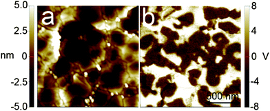 | ||
| Fig. 10 Left: 1.5 × 1.5 μm2C-AFM topography image. Right: the same area scanned using piezoelectric force microscopy, showing the piezoelectric domain structure of a LiNbO3 thin film deposited on a silicon substrate using 666 super-cycles each consisting of two cycles of Nb(OEt)5 and H2O and one cycle of LiN(SiMe3)2 and H2O, thereafter annealed for 15 min at 650 °C. The back contacts were made of silver paint. | ||
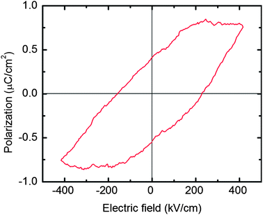 | ||
| Fig. 11 Measured ferroelectric hysteresis loop measured at 1 kHz for a 120 nm thick LiNbO3 film on a silicon substrate with electrical contacts made from silver paint. | ||
Discussion
In order to reproducibly achieve the targeted LiNbO3 films it was proved necessary to always deposit 2000 cycles of Nb2O5 between each deposition with high lithium content. Several attempts were made to reproduce the sample closest to the stoichiometric composition after the following scheme: (a) verify the growth of Nb2O5, (b) test LiNbO3 deposition and (c) deposit LiNbO3 on single crystal substrates. Parts (a) and (b) always worked while (c) always failed, meaning that it proved impossible to deposit two successive deposition of LiNbO3 after breaking the vacuum. No detailed analysis was made of the failed runs, yet ellipsometry measurements yielded too high refractive index compared to the one previously obtained for the stoichiometric phase, and XRD shows niobium rich phases of Nb2O5 and LiNb3O8. Even if the stoichiometry was not reproduced, the films were still uniform and no powders were formed. Experiments with alternating deposition of LiNbO3 and Nb2O5 were always successful, and this was then adopted as the standard protocol. We note that deviation from the expected stoichiometry always resulted in more niobium rich samples, which were uniform, with no powder formation and in the expected thickness range. One may speculate whether a likely mechanism is that the lithium containing material absorbs water during the water pulse and releases water during the metal pulse, through the so-called reservoir effect, a similar case was recently found by Comstock and Elam when studying the reaction mechanisms of Li–Al–O deposition.42 Why this shifts the stoichiometry towards the niobium rich side requires further investigations.The surface layer of the LiNbO3 samples is dominated by Li2CO3 which is consistent with an observed enrichment of lithium on the surface. The depth profiles from TOF-ERDA show that the lithium to niobium ratio is constant throughout the film, except on the very surface. This suggests that lithium ions are mobile and diffuse even at room temperature, ruled by the chemical potentials of CO2 and H2O in ambient air. Our hypothesis is that an excess of lithium species on the surface is the origin of uncontrolled growth, based on the observations so far. The excess lithium on the surface of the chamber may either be caused by consecutive lithium cycles or by Li-diffusion throughout the deposited film when exposed to ambient air. This behaviour may also be transferrable to other deposition processes of lithium compounds by ALD.
The LiNbO3 films have a strong tendency to order epitaxially on substrates such as LaAlO3 and Al2O3. Epitaxial ordering is expected as the structures are similar and the lattice mismatch is 1.2 and 3.9% for LaAlO3 and r-Al2O3 respectively, when assuming pseudocubic unit cells with cell parameters of 3.79 and 3.48 Å, respectively, when compared to 3.76 Å for LiNbO3. On the structurally very similar Al2O3 and LaAlO3, the orientation of the thin film is selective as shown in Fig. 5–8. The lack of observed selective ordering on SrTiO3 is believed to stem from a difference in octahedral tilt, as SrTiO3 has no octahedral tilt (SG Pm-3m), compared to a (a−, a−, a−)-tilt in LaAlO3 and a stronger tilt of the same type in LiNbO3. In any case, depending on the substrate, control of orientation is achieved. LaAlO3 does order on SrTiO3 but even though the type of tilt is similar to LiNbO3, the amount of tilt is very large in LiNbO3 compared to LaAlO3.
The coercive field for the LiNbO3 thin films is around 220 kV cm−1. This is comparable to earlier reported values for congruent LiNbO3. The ferroelectric domains are pure and domain walls are well defined as shown by PFM-measurements. It is likely that the coercive field can be engineered by varying the stoichiometry of the LiNbO3 thin films, which would open up for tailoring features for a range of applications.
Conclusion
Epitaxial thin films of ferroelectric LiNbO3 have been deposited with ALD. The films have been analyzed using X-ray- and ion-scattering techniques, ellipsometry, and scanning probe microscopy as well as by ferroelectric characterization. Fundamental issues connected with deposition of lithium containing oxides have been identified and discussed, especially possible limitations in the lithium content and room temperature diffusion of lithium.References
- B. T. Matthias and J. P. Remeika, Phys. Rev., 1949, 76, 1886–1887 CrossRef.
- K. Nassau, H. J. Levinstein and G. M. Loiacono, J. Phys. Chem. Solids, 1966, 27, 989–996 CrossRef CAS.
- R. A. Graham, Ferroelectrics, 1976, 10, 65–69 CrossRef CAS.
- A. Savage, J. Appl. Phys., 1966, 37, 3071–3072 CrossRef CAS.
- R. W. Dixon and M. G. Cohen, Appl. Phys. Lett., 1966, 8, 205–207 CrossRef CAS.
- D. B. Fraser and A. W. Warner, J. Appl. Phys., 1966, 37, 3853–3854 CrossRef CAS.
- E. L. Wooten, K. M. Kissa, A. Yi-Yan, E. J. Murphy, D. A. Lafaw, P. F. Hallemeier, D. Maack, D. V. Attanasio, D. J. Fritz, G. J. McBrien and D. E. Bossi, IEEE J. Sel. Top. Quantum Electron., 2000, 6, 69–82 CrossRef CAS.
- A. Grisard, E. Lallier, G. Garry and P. Aubert, IEEE J. Quantum Electron., 1997, 33, 1627–1635 CrossRef CAS.
- H. Jelinkova, J. Sulc, P. Koranda, M. Nemec, M. Cech, M. Jelinek and V. Skoda, Laser Phys. Lett., 2004, 1, 59–64 CrossRef CAS.
- K. Gallo, G. Assanto, K. R. Parameswaran and M. M. Fejer, Appl. Phys. Lett., 2001, 79, 314–316 CrossRef CAS.
- J. L. Jackel, C. E. Rice and J. J. Veselka, Appl. Phys. Lett., 1982, 41, 607–608 CrossRef CAS.
- Y. Kawata, H. Ishitobi and S. Kawata, Opt. Lett., 1998, 23, 756–758 CrossRef CAS.
- Y. Kawata, H. Ueki, Y. Hashimoto and S. Kawata, Appl. Opt., 1995, 34, 4105–4110 CrossRef CAS.
- V. Gopalan, T. E. Mitchell, Y. Furukawa and K. Kitamura, Appl. Phys. Lett., 1998, 72, 1981–1983 CrossRef CAS.
- D. W. Chapman, J. Appl. Phys., 1969, 40, 2381–2385 CrossRef CAS.
- P. Muralt, J. Micromech. Microeng., 2000, 10, 136–146 CrossRef CAS.
- S. S. Gevorgian and E. L. Kollberg, IEEE Trans. Microwave Theory Tech., 2001, 49, 2117–2124 CrossRef CAS.
- Y. Arimoto and H. Ishiwara, MRS Bull., 2004, 29, 823–828 CrossRef CAS.
- N. Setter, D. Damjanovic, L. Eng, G. Fox, S. Gevorgian, S. Hong, A. Kingon, H. Kohlstedt, N. Y. Park, G. B. Stephenson, I. Stolitchnov, A. K. Taganstev, D. V. Taylor, T. Yamada and S. Streiffer, J. Appl. Phys., 2006, 100, 051606 CrossRef.
- G. Oszlánczi, A. Papp, A. Szabó, L. Nagymajtényi, A. Sápi, Z. Kónya, E. Paulik and T. Vezér, Inhalation Toxicol., 2011, 23, 173–181 CrossRef.
- Y. Shibata, K. Kaya, K. Akashi, M. Kanai, T. Kawai and S. Kawai, Appl. Phys. Lett., 1992, 61, 1000–1002 CrossRef CAS.
- S. B. Ogale, R. Nawathey-Dikshit, S. J. Dikshit and S. M. Kanetkar, J. Appl. Phys., 1992, 71, 5718–5720 CrossRef CAS.
- R. A. Betts and C. W. Pitt, Electron. Lett., 1985, 21, 960–962 CrossRef CAS.
- T. Aaltonen, M. Alnes, O. Nilsen, L. Costelle and H. Fjellvag, J. Mater. Chem., 2010, 20, 2877–2881 RSC.
- T. Aaltonen, O. Nilsen, A. Magraso and H. Fjellvag, Chem. Mater., 2011, 23, 4669–4675 CrossRef CAS.
- J. Hämäläinen, F. Munnik, T. Hatanpää, J. Holopainen, M. Ritala and M. Leskela, J. Vac. Sci. Technol., A, 2012, 30, 01A106 Search PubMed.
- M. Putkonen, T. Aaltonen, M. Alnes, T. Sajavaara, O. Nilsen and H. Fjellvag, J. Mater. Chem., 2009, 19, 8767–8771 RSC.
- J. Hämäläinen, J. Holopainen, F. Munnik, T. Hatanpaa, M. Heikkila, M. Ritala and M. Leskela, J. Electrochem. Soc., 2012, 159, A259–A263 CrossRef.
- M. E. Donders, H. C. M. Knoops, W. M. M. Kessels and P. H. L. Notten, ECS Trans., 2011, 41, 321–330 CrossRef CAS.
- E. Østreng, P. Vajeeston, O. Nilsen and H. Fjellvåg, RSC Adv., 2012, 2, 6315–6322 RSC.
- J. Harjuoja, A. Kosola, M. Putkonen and L. Niinistoe, Thin Solid Films, 2006, 496, 346–352 CrossRef CAS.
- J. Harjuoja, S. Vaeyrynen, M. Putkonen, L. Niinistoe and E. Rauhala, Appl. Surf. Sci., 2007, 253, 5228–5232 CrossRef CAS.
- M. Vehkamäki, T. Hatanpaeae, M. Kemell, M. Ritala and M. Leskelae, Chem. Mater., 2006, 18, 3883–3888 CrossRef.
- J. Muller, U. Schroder, T. S. Boscke, I. Muller, U. Bottger, L. Wilde, J. Sundqvist, M. Lemberger, P. Kucher, T. Mikolajick and L. Frey, J. Appl. Phys., 2011, 110, 114113–114115 CrossRef.
- M. Bjorck and G. Andersson, J. Appl. Crystallogr., 2007, 40, 1174–1178 CrossRef.
- K. Kukli, M. Ritala, M. Leskelä and R. Lappalainen, Chem. Vap. Deposition, 1998, 4, 29–34 CAS.
- L. O. Svaasand, M. Eriksrud, G. Nakken and A. P. Grande, J. Cryst. Growth, 1974, 22, 230–232 CrossRef CAS.
- H. H. Sønsteby, E. Østreng, O. Nilsen and H. Fjellvåg, Thin Solid Films, 2013 Search PubMed , submitted.
- H. F. Wang, Y. Y. Zhu, S. N. Zhu and N. B. Ming, Appl. Phys. A: Mater. Sci. Process., 1997, 65, 437–438 CrossRef CAS.
- J. H. Ro, O.-Y. Jeon, T.-H. Kim, J.-H. Ro and M. Cha, Ferroelectrics, 2002, 269, 231–236 CAS.
- S.-W. Jung, Y.-S. Kim, S.-H. Jeong, Y.-I. In, K.-H. Kim and K. No, J. Korean Phys. Soc., 2003, 42, 1386–1390 Search PubMed.
- D. J. Comstock and J. W. Elam, J. Phys. Chem. C, 2012, 117, 1677–1683 Search PubMed.
Footnote |
| † Electronic supplementary information (ESI) available. See DOI: 10.1039/c3tc30271g |
| This journal is © The Royal Society of Chemistry 2013 |