
Optical color routing enabled by deep learning
Shijie
Xiong
and
Xianguang
Yang
 *
*
Guangdong Provincial Key Laboratory of Nanophotonic Manipulation, Institute of Nanophotonics, College of Physics & Optoelectronic Engineering, Jinan University, Guangzhou 511443, China. E-mail: xianguang@jnu.edu.cn
First published on 21st March 2024
Abstract
Nano-color routing has emerged as an immensely popular and widely discussed subject in the realms of light field manipulation, image sensing, and the integration of deep learning. The conventional dye filters employed in commercial applications have long been hampered by several limitations, including subpar signal-to-noise ratio, restricted upper bounds on optical efficiency, and challenges associated with miniaturization. Nonetheless, the advent of bandpass-free color routing has opened up unprecedented avenues for achieving remarkable optical spectral efficiency and operation at sub-wavelength scales within the area of image sensing applications. This has brought about a paradigm shift, fundamentally transforming the field by offering a promising solution to surmount the constraints encountered with traditional dye filters. This review presents a comprehensive exploration of representative deep learning-driven nano-color routing structure designs, encompassing forward simulation algorithms, photonic neural networks, and various global and local topology optimization methods. A thorough comparison is drawn between the exceptional light-splitting capabilities exhibited by these methods and those of traditional design approaches. Additionally, the existing research on color routing is summarized, highlighting a promising direction for forthcoming development, delivering valuable insights to advance the field of color routing and serving as a powerful reference for future endeavors.
 Shijie Xiong | Shijie Xiong is a student under the guidance of Xianguang Yang, pursuing his master's degree at the Institute of Nanophotonics, Jinan University, China. His research interests mainly focus on nanophotonic devices and deep learning applications. |
 Xianguang Yang | Xianguang Yang is an Associate Professor at the Institute of Nanophotonics, College of Physics & Optoelectronic Engineering, Jinan University, China. His research interests focus on low-dimensional optoelectronic materials and device applications. |
Introduction
Image sensor color routing has attracted heightened attention across various domains including facial recognition, autonomous navigation, virtual reality, and academic research, with deep learning technology serving as a promising complement.1 Equipped with formidable capabilities in pattern recognition,2 optimization strategies,3 and adaptive reverse engineering methodologies,4 deep learning can adeptly process and analyze intricate spectral data generated by color routing, which enables the identification of subtle features and patterns within light signals across various wavelengths. This facilitates extensive training and meticulous parameter selection based on anticipated spectral attributes, and ultimately optimizes the achievement of the desired color routing structure by learning the underlying mapping between spectra and color routing structures.5,6 In more detail, color management in image sensors encompasses spectral truncation and spatially guided propagation of incident broadband light.7,8 Dye filters currently reign as the predominant color realization technology in the realm of image sensors, capitalizing on the transmission and absorption characteristics of organic materials.9,10 As shown on the left panel of Fig. 1d, a back-illumination CMOS image sensor consists of microlenses and an RGB color filter array. In Fig. 1b, nanostructured color filters based on uniform-height amorphous silicon structures are designed and optimized, accompanied by a submicron-sized RGB filter array reduced to 0.5 μm. Specifically, they selectively propagate light within the targeted spectral range while attenuating light across other spectral domains.11 Nevertheless, as imaging pixel sizes continue to diminish, there is an urgent demand for enhanced unit pixel signal-to-noise ratios, improved optical and photoelectric conversion efficiencies, and effective noise suppression. Conventional dye filters and traditional filtering methodologies based on micro- and nanostructures fall short in meeting these stringent requirements.12–15 In this context, the concept of nano-color routing has emerged. Specifically, some structures, leveraging the meta-lensing effect, can focus light on extremely small regions at the nanoscale, enabling precise directional manipulation and control of light, thereby enhancing optical efficiency.16–19 In Fig. 1a, a V-shaped all-dielectric wavelength router can effectively control the incident light by scattering it into two different wavelengths (λ1 = 755 nm and λ2 = 660 nm). The routing of spatial light is primarily determined by the distribution of the refractive index in three-dimensional space. As demonstrated by Fig. 1c and the right panel of Fig. 1d, R-G1-B-G2 color routing is manifested by integrating into a square with dimensions of 11.55 μm × 11.55 μm with a 4 μm focal length, showing three distinct meta-lenses with respective wavelength λd values of 430, 532, and 633 nm. Henceforth, nano-optical structures exhibit the capability of achieving precise phase modulation at the nanoscale. In particular, techniques such as grating diffraction,20 surface plasmon resonances in metal nanostructures,21,22 dielectric nanoantennas,23,24 and metasurfaces and metamaterials25,26 can be designed based on phase modulation. These structures enable the manipulation of the wavefront of light through the transmission phase, geometric phase, or resonance phase, thereby achieving spatial dispersion of optical beams. Furthermore, with the neural networks being trained on large-scale spectral data and benefiting from self-feedback mechanisms, the spectral splitting capability of nanoscale color routing can be well enhanced, and the emerging deep learning-enabled optical color routing holds promise in opening new avenues for future research.27,28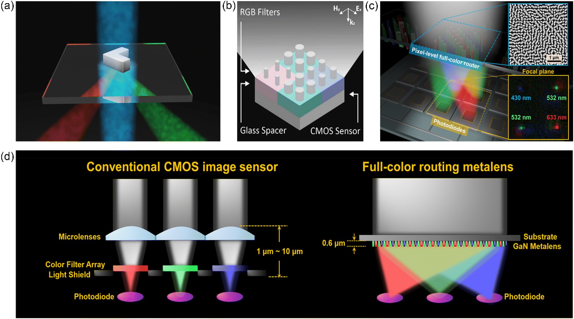 | ||
| Fig. 1 Different image sensor filtering strategies and color routing mechanisms. (a) V-shaped all-dielectric antenna wavelength router. Reproduced with permission.29 Copyright © 2016 American Chemical Society. (b) Sub-micrometer nanostructure-based RGB filters for CMOS image sensors. Reproduced with permission.30 Copyright © 2019 American Chemical Society. (c) R-G1-B-G2 full-color routing with multiplex GaN metalens.31 (d) Schematic of a conventional CMOS image sensor and metalens-based color router. Reproduced with permission.31 Copyright © 2017 American Chemical Society. | ||
Nanophotonic spectral sorting
The essence of nano-color routing lies in the dispersion and precise guidance of light, with its functionality intricately intertwined with the art of spectral manipulation.32 In the realm of nanophotonics, spectral strategies encompass techniques consisting of grating diffraction color separation, plasmonic mechanisms, metasurface arrays, and dielectric nanoantenna color separation.33–35 The scattering behavior of nanostructures is intrinsically wavelength-sensitive. Besides the spectral control engendered by surface plasmon resonance in metallic nanostructures, additional light routing effects can be achieved through wavelength-dependent scattering in conjunction with the effective reflection resulting from the placement of dielectric nano-pillars just above the pixel interface of image sensors.36,37 In Fig. 2e, an SiN-based metalens array exhibits average optical efficiencies of 64%, 75%, and 94% at wavelengths of 430, 520, and 635 nm, respectively, through the entire RGB areas, which greatly exceed the upper limits of the optical efficiencies of the filter array for Bayer pixel arrangements (∼33%). More impressively, as demonstrated in Fig. 2f, the pixel-level Bayer-type color router holds the color collection efficiencies of 58, 59, and 49% at wavelengths of 640, 540, and 460 nm, representing R, G and B pixels, respectively. Using a 200 μm sized array working with a monochromatic imaging sensor, the image intensity reaches twice that achieved using a Bayer color filter. Accordingly, both endeavors have succeeded in enhancing the optical efficiency on using Bayer array image sensors. At the same time, other implementations including multilayer-disordered semiconductor routing arrays, and structurally irregular monolayer spectral routers also demonstrated commendable optical efficiency. In Fig. 2a, a novel color routing scheme with an irregular dielectric structure is designed with a pixel size of 800 nm. Clever pixel arrangement cyclically distributes red, green, and blue pixels, reducing simulation time and achieving a notable improvement of over 80% in optical efficiency. The irregular structure of the color routing model can be observed more intuitively through the quarter-array region denoted by the yellow dashed box in Fig. 2b. More profoundly, a three-dimensional dielectric color scatter, composed of SiO2 and TiO2 materials, was fabricated, exhibiting over 70% efficiency across the entire visible spectrum (400 nm–700 nm) among three subpixels (red, green, and blue) as depicted in Fig. 2c. In Fig. 2d, a breakthrough in color routing was achieved with a multilayer SiO2 array, showcasing a novel advancement by standard lithography and material deposition. However, as optical structures venture into submicron and even nanometer scales, the simplistic ray optics theories may no longer be applicable.38,39 At this point, simulation methods based on traditional finite element or finite difference in time domains often yield only locally optimized solutions, posing various bottlenecks at the practical application level. Recently, the rapid advancement of deep learning has injected new spirit into the field of nanophotonics research.40,41 The deep learning approach, known for its efficient optimization across the entire parameter space, has recently emerged as a major focal point of research interest.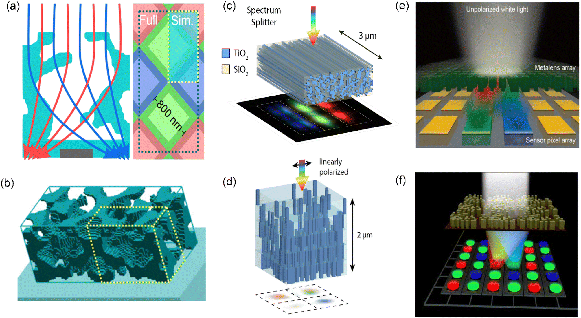 | ||
| Fig. 2 Color routing mechanisms in different implementation forms. (a) A new type of splitter composed of irregular structures.42 (b) Top view of the color-coded layers for an irregular-layer topology-optimized splitter structure. Reproduced with permission.42 Copyright © 2021 Elsevier. (c) Spectrum splitter consisting of TiO2 bars and SiO2 substrates. Reproduced with permission.43 Copyright © 2019 IEEE. (d) Multilayer-designed spectral router fabricated by lithography and material deposition. Reproduced with permission.44 Copyright © 2020 The Optical Society. (e) Schematic of an image sensor with a full-color-sorting metalens array. Reproduced with permission.45 Copyright © 2021 Optica Publishing Group. (f) Pixel-level Bayer-type color router based on metasurfaces. Reproduced with permission.46 Copyright © 2022 Springer Nature. | ||
Deep learning-enabled engineering
In recent years, the field of optics has witnessed remarkable advancements propelled by the advent of deep learning technology.47 Generally, in the optimization design process of color routing, deep learning is typically applied by first collecting a large amount of spectral data for processing and analysis, aiming to extract valuable mapping relationships through training.48 Subsequently, the corresponding optimization parameters need to be formulated, typically reflecting the optical efficiency of spectral splitting for each pixel channel in the color routing problem. Finally, through a combination of strategies, such as gradient descent optimization using neural networks or multi-objective optimization algorithms, the color routing structure tends to be iteratively optimized towards the desired outcome.49,50 Specifically in other applications, from image recognition, pattern identification, and image reconstruction in optical imaging to the efficient optimization of inverse design on the micro- and nanostructures, and further into domains such as optical signals, photonics communication, and laser technology, the flexibility and precision of deep learning have infused new spirits and possibilities into optical research and applications.51–55Fig. 3a illustrates a multispectral imaging system based on a diffractive optical network. Through deep learning training, this system can create a virtual spectral filter array in the output image field, transforming a monochrome focal plane array into a multispectral imaging device without any spectral filters or image recovery algorithms. This system achieves snapshot multispectral imaging with 4, 9 and 16 unique spectral bands within the visible spectrum, with a compact design that axially spans ∼72λm (λm represents the mean wavelength of the spectral band of interest). Also, deep learning plays a pivotal role in the simulation and inverse design of individual nano-optical particles. As indicated in Fig. 3b, an artificial intelligence neural network was trained with 50![[thin space (1/6-em)]](https://www.rsc.org/images/entities/char_2009.gif) 000 examples using a learning rate of 0.0006 and a decay of 0.99. This network predicts the thickness of nano-shell structures with high precision, achieving comparable accuracy of over ∼90% to traditional simulations with minimal training data. While currently applied to nano-shell structure prediction, the demonstrated potential of this method extends to various inverse design problems. Similarly, this avant-garde inverse prediction method is highly popular in the metasurface domain. The metasurface design often involves elemental atoms, requiring repeated trial and error to achieve the desired electromagnetic response. The conventional design process, entailing numerous physical and geometric parameters, demands significant computational resources.56,57 As highlighted in Fig. 3c, the meta-atom data were randomly split into training and test data sets, with 70% data used during the training process and the remaining 30% data used to evaluate the trained network. The average mean squared error (MSE) for the real and imaginary parts of the predicted coefficients in the test data were 0.00035 and 0.00023, respectively, which dramatically reduces representation time while ensuring accuracy. In Fig. 3d and e, another model, deep neural network (DNN), predicts the geometric shape of nanostructures by collecting the far-field response spectrum. This method can be extended to predict other physical or optical parameters of host materials and compounds, addressing inverse problems that conventional methods struggle to resolve. In the field of chemistry, a DL model has been proposed to predict the optical and physical properties of organic compounds. This model, trained on a dataset of 30094 luminescent groups, successfully achieves effective prediction and screening, as illustrated in Fig. 3f. Another core application of deep learning is dedicated to the realm of optical storage and computation. For this purpose, a geometric information encoding scheme for subwavelength dielectric nanostructures has been introduced. Building neural networks based on over 40000 scattering spectra of these structures, it ultimately achieves a readout accuracy of >99%, with sequences of up to 9 bits as shown in Fig. 3g. This paves the way for high-density optical information storage in planar silicon nanostructures.
000 examples using a learning rate of 0.0006 and a decay of 0.99. This network predicts the thickness of nano-shell structures with high precision, achieving comparable accuracy of over ∼90% to traditional simulations with minimal training data. While currently applied to nano-shell structure prediction, the demonstrated potential of this method extends to various inverse design problems. Similarly, this avant-garde inverse prediction method is highly popular in the metasurface domain. The metasurface design often involves elemental atoms, requiring repeated trial and error to achieve the desired electromagnetic response. The conventional design process, entailing numerous physical and geometric parameters, demands significant computational resources.56,57 As highlighted in Fig. 3c, the meta-atom data were randomly split into training and test data sets, with 70% data used during the training process and the remaining 30% data used to evaluate the trained network. The average mean squared error (MSE) for the real and imaginary parts of the predicted coefficients in the test data were 0.00035 and 0.00023, respectively, which dramatically reduces representation time while ensuring accuracy. In Fig. 3d and e, another model, deep neural network (DNN), predicts the geometric shape of nanostructures by collecting the far-field response spectrum. This method can be extended to predict other physical or optical parameters of host materials and compounds, addressing inverse problems that conventional methods struggle to resolve. In the field of chemistry, a DL model has been proposed to predict the optical and physical properties of organic compounds. This model, trained on a dataset of 30094 luminescent groups, successfully achieves effective prediction and screening, as illustrated in Fig. 3f. Another core application of deep learning is dedicated to the realm of optical storage and computation. For this purpose, a geometric information encoding scheme for subwavelength dielectric nanostructures has been introduced. Building neural networks based on over 40000 scattering spectra of these structures, it ultimately achieves a readout accuracy of >99%, with sequences of up to 9 bits as shown in Fig. 3g. This paves the way for high-density optical information storage in planar silicon nanostructures.
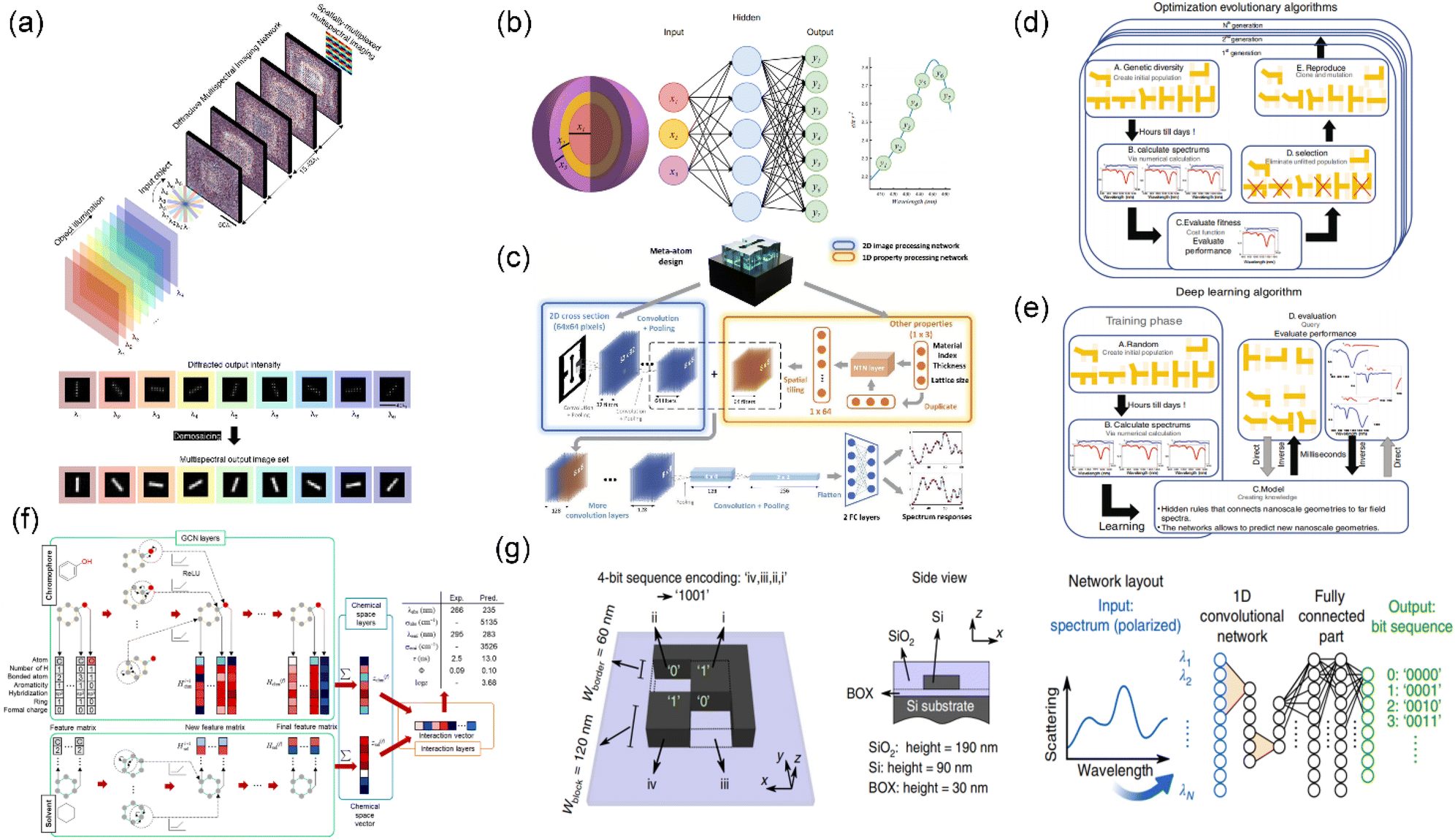 | ||
| Fig. 3 Relevant achievements and progress of various deep learning technologies in the field of optics. (a) Diffractive optical network-based multispectral imaging system. Reproduced with permission.58 Copyright © 2023 Springer Nature. (b) A method using artificial neural networks to approximate light scattering by multilayer nanoparticles. Reproduced with permission.59 Copyright © 2018 AAAS. (c) CNN-based model aiming at modeling meta-atoms with high degrees of freedom. Reproduced with permission.60 Copyright © 2020 The Optical Society. (d and e) Deep neural network-enabled plasmonic nanostructure design. Reproduced with permission.61 Copyright © 2018 Springer Nature. (f) Deep learning optical spectroscopy applied in molecular design. Reproduced with permission.62 Copyright © 2021 American Chemical Society. (g) The deep learning method used in increasing optical information storage. Reproduced with permission.63 Copyright © 2019 Springer Nature. | ||
Algorithm-driven spectroscopic optimization
Traditional optical simulation and optimization strategies are closely associated with methods such as physical optics, ray tracing, and electromagnetic field solvers, especially when studying nanophotonic devices or optical waveguides at the microscopic scale.64,65 The electromagnetic field equations, such as Maxwell's equations, are commonly employed to simulate the propagation and interactions of light. Numerical methods like the finite element method (FEM) and finite difference time domain (FDTD) have traditionally been prevalent for solving these equations.66 However, with the continual shift in computing capabilities and numerical algorithm paradigms, algorithm-assisted design for nanoscale color routing has garnered widespread attention in recent years. In the realm of holographic optical design, algorithmic optimization for controlling the wavefront of light has allowed precise phase modulation on nanostructures, enabling highly customized dispersion effects. This method opens up new possibilities for the creation of high-performance nanoscale color routing devices. Specifically, in the optimization of nanoscale color routing designs, the application of algorithms like genetic algorithms, particle swarm optimization, and simulated annealing makes finding the optimal color routing schemes in complex optical systems more feasible.67–69 Taking genetic algorithms as an example, the optical efficiency of each pixel in color routing becomes the global optimization target. Through multiple iterations with the initialization, fitness calculation, crossover, and mutation operations, the algorithm converges to the region of optimal output, as depicted in Fig. 4a–c. In Fig. 4a, the 1 μm-pixel-sized color router achieves algorithm optimization through a 16 × 16 nanopillar encoding strategy, of which the termination condition is set such that the global fitness function value is less than ∼1 × 10⁻⁶ within every 2000 solutions of 200 iterations. Similarly, Fig. 4b adopts a 0–1 encoding method, mapping the routing array into a continuous RGB arrangement of 11 × 33, achieving over 60% optical efficiency improvement in every RGB channel. As shown in Fig. 4c, the specific implementation process of the genetic algorithm originates from the continuous selection, iteration, and sorting of lold and lnew values. However, globally optimized results obtained through genetic algorithms may still leave room for improvement in the optical efficiency of individual pixels. Local optimization strategies, inspired by deep learning models based on local gradient descent, can further refine the results. As illustrated in Fig. 4d, a lossless device implementing RGB-IR four-channel pixel color routing adopts a gradient-based optimization method, achieving nearly perfect color routing with width dimensions smaller than 400 nm. The color channels are defined by the central wavelengths, which serve as the point peak of optical efficiency or center of the spectral band, i.e. blue (450 nm), green (550 nm), red (650 nm), and NIR (750 nm), while each channel is perfect with simulation optical efficiency of >0.99 and optical crosstalk of <0.01. More intriguingly, some accompanying optimization methods in deep learning combine multiple different models to obtain greater parameter space flexibility.70,71 They achieve dimensionality reduction for complex multidimensional optimization problems through techniques such as convolution, pooling, and deconvolution, which greatly enhance the feasibility of synchronous optimization of images and spectra in color routing design. Specifically, a deep learning model called UCNN, based on adjoint optimization, was employed to learn the correlation between far-field amplitude phase patterns and subwavelength images, achieving the accurate recognition of hand-written digits from 0 to 9, as shown in Fig. 4e. The training data of this model including input images taken from the MINIST database of handwritten digits (70000 images with (20 × 20)-pixel resolution) were eventually down-sampled into 8 × 8 pixels reaching a classification accuracy of 97.5%. Addressing spectral optimization challenges at the algorithmic level, deep learning function interpretation proves more capable of reflecting implicit connections between structural parameters and optical responses. In Fig. 4f, a proposed convolutional correlator neural network (CCNN) serves as a non-linear architecture generating features that can interpret class image data effectively, demonstrating excellent model generalization capabilities for recognizing images with random structures in the red, green, and blue color routing channels.
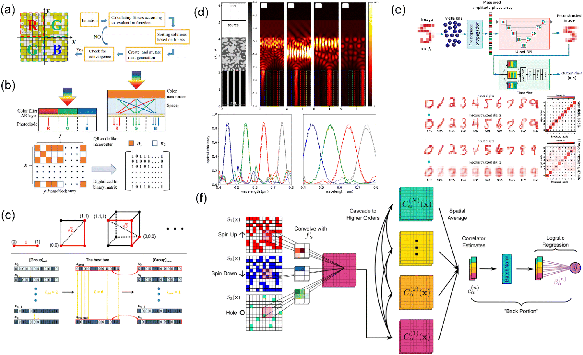 | ||
| Fig. 4 Optical splitting routing design under different optimization strategy designs. (a) Bayer-array color routing optimized using the genetic algorithm. Reproduced with permission.40 Copyright © 2022 Springer Nature. (b) A single-layer QR-code-like nano-color router enhanced using the NSGA-II algorithm.72 (c) Ultracompact color splitter driven by an inverse design genetic algorithm. Reproduced with permission.73 Copyright © 2022 American Chemical Society. (d) RGB-IR router optimized by gradient-based optimization combined with an FDTD solution. Reproduced with permission.74 Copyright © 2021 John Wiley and Sons. (e) The deep neural network for far-field recognition of subwavelength image sensor optimization. Reproduced with permission.75 Copyright © 2020 American Physical Society. (f) The correlator convolutional neural network architecture used in image reconstruction optimization. Reproduced with permission.76 Copyright © 2021 Springer Nature. | ||
Structure prediction and inverse design of nanophotonics
The design of nanophotonic color routing relies heavily on structural simulation and prediction, typically involving techniques such as computational modeling, numerical analysis, and algorithm optimization.77,78 The inverse design strategy in deep learning has broad and profound implications for optimizing color routing. Typically, in the inverse design process, the forward networks were employed to train and learn the potential mapping relationships between label quantities and images, which precisely reflects upon the corresponding structures and spectra in color routing.79 Conversely, the reverse networks focus on feedback loss values to evaluate the quality of training results, which often determines the performance superiority or inferiority of the final design structure in color routing.80,81 Through such a combined forward and reverse method, the inverse design process of color routing is thus succinctly interpreted. However, traditional simulation processes mainly entail modeling the electromagnetic behavior and optical performance of structures, followed by predictions in the optical domain.82 This process often necessitates addressing multiple physical field couplings, including thermal and mechanical considerations, leading to intricate computations and substantial workloads.83 To address these challenges, deep learning techniques have been introduced with the aim of achieving more efficient and precise optimization of nanophotonic structures. At the deep learning level, one widely employed model is that of the convolutional neural network (CNN), a forward-propagating neural network that extracts features from input data for classification or regression.84,85 CNNs are commonly applied to image processing tasks, utilizing convolutional layers, pooling layers, and fully connected layers to learn features inherent in input data. In contrast, the focus of inverse design methods is on optimizing objectives, making them particularly attractive for nanophotonic color routing and associated optimization problems. Given the known outputs or performance criteria, these methods involve training to establish mapping relationships between latent variables, optimizing design parameters to achieve the optimal performance of specific devices.86,87 As illustrated in Fig. 5a, a deep neural network designed for a power splitter based on a compact (2.6 × 2.6 μm2) silicon-on-insulator (SOI) chip demonstrates minimized reflection (below −20 dB), achieving over 90% maximum transmission efficiency and the desired splitting characteristics. Similarly, another inverse design approach has shown significant effectiveness in predicting structural colors based on Fabry–Perot (F–P) cavity structures. This method utilizes a bidirectional artificial neural network to generate a broader color space coverage exceeding 125% of sRGB, demonstrating high accuracy (as shown in Fig. 5b). Both of these inverse design solutions, based on spectral datasets related to transmission or scattering, showcase the effectiveness of inverse design in optimizing nanophotonic structures. In another work, a generative adversarial network (GAN) model based on an absorption spectral dataset (consisting of 20000 metasurface unit cell designs) is proposed for optimizing the designs of plasmonic and dielectric metasurfaces (as shown in Fig. 5c). The mentioned DCGAN model exhibits good generalization capabilities in both image and spectral generation (maintained accuracy ∼90%). By training the generator to establish the mapping relationship between input data and random latent vectors (200-dimensional column vector), and iteratively refining the results through error backpropagation with the discriminator, the model achieves structures that closely approach the optimization objectives. This work undoubtedly represents a notable application of deep learning in the inverse design of nanophotonic structures, offering constructive insights into the inverse design of nanophotonic color routing.
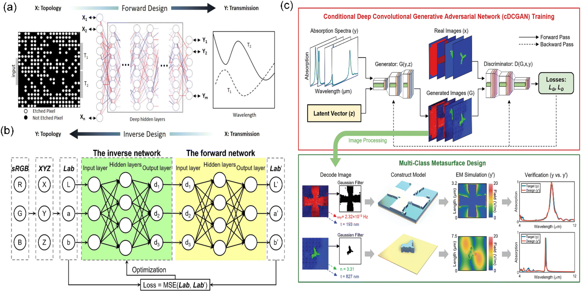 | ||
| Fig. 5 Application of inverse design methods in the field of photonics. (a) Deep neural network inverse design of the integrated photonic power splitter. Reproduced with permission.88 Copyright © 2019 Springer Nature. (b) Inverse design of the Fabry-Perot cavity-based color filter using the bidirectional artificial neural network. Reproduced with permission.89 Copyright © 2021 Optica Publishing Group. (c) Global inverse design across multiple photonic structure classes using generative deep learning. Reproduced with permission.90 Copyright © 2021 John Wiley and Sons. | ||
Outlook and perspective
In summary, this paper extensively explores color separation technologies in various image sensors, ranging from traditional commercial dye filters to plasmonic metasurfaces, nanoantenna arrays, and algorithmically supported color routing designs. The analysis of this comprehensive review leads to the conclusion that wavelength-correlated spatial routing for color separation technology has advantages over traditional color filtering techniques, particularly in terms of high optical flux.91 It also holds potential application value for the continuous development of high-pixel-density image sensors. The study of multi-wavelength spatial routing at the submicron scale is of significant academic importance for advancing novel optical field control technologies in micro- and nano-optics.92 From the reported research results, it is evident that, compared to macroscopic diffraction gratings, both metallic nanostructures and dielectric nanostructures, based on pattern coupling and phase mutation mechanisms, can achieve miniaturized spatial color separation.93 These structures possess the potential for pixel-level integration on image sensors, theoretically providing 2 to 4 times the optical flux.94 This issue has not only attracted considerable attention from the academic community but has also ignited research and development enthusiasm among major players in the image sensor industry. Furthermore, this review delves into the current state of development of color routing technology based on deep learning, analyzing the superiority gained by overcoming bottlenecks of traditional color separation techniques through the introduction of deep learning methods. Simultaneously, the discussions on spectral sorting, deep learning-assisted engineering, algorithm-based spectral optimization, and the prediction and reverse design of nano-optical structures reveal the latent advantages and innovation of deep learning in color routing design.95,96 In conclusion, this review provides readers with a comprehensive understanding of the application of deep learning technology in the field of nano-color routing. It emphasizes the crucial role of deep learning in nanophotonics and anticipates future directions in this field. We look forward to witnessing more exciting discoveries and innovations in this cutting-edge domain, providing a reference for the development of next-generation, high-performance color routing.Data availability
The data supporting this study are available from the corresponding author upon reasonable request.Conflicts of interest
The authors declare no competing financial interest.Acknowledgements
This work was supported by the National Natural Science Foundation of China (11804120), the Guangdong Basic and Applied Basic Research Foundation (2023A1515030209), the Research Projects from Guangzhou (2023A03J0018), and the Fundamental Research Funds for the Central Universities (21623412).References
- J. He and B. Zhou, A Deep Learning-Assisted Visible Light Positioning Scheme for Vehicles With Image Sensor, IEEE Photonics J., 2022, 14, 4 Search PubMed.
- S. M. Man and B. J. Jenkins, Context-dependent functions of pattern recognition receptors in cancer, Nat. Rev. Cancer, 2022, 22, 7 CrossRef PubMed.
- H. T. Kollmann, D. W. Abueidda and S. Koric, et al., Deep learning for topology optimization of 2D metamaterials, Mater. Des., 2020, 196, 109098 CrossRef.
- M. Dijkstra and E. Luijten, From predictive modelling to machine learning and reverse engineering of colloidal self-assembly, Nat. Mater., 2021, 20, 6 CrossRef PubMed.
- X. Cao, Y. Du and Y. Guo, et al., Replicating the Cynandra opis butterfly's structural color for bioinspired bigrating color filters, Adv. Mater., 2022, 34, 9 Search PubMed.
- J. L. Lansford and D. G. Vlachos, Infrared spectroscopy data-and physics-driven machine learning for characterizing surface microstructure of complex materials, Nat. Commun., 2020, 11, 1513 CrossRef CAS PubMed.
- W. Wang and L. Qi, Light management with patterned micro and nanostructure arrays for photocatalysis, photovoltaics, and optoelectronic and optical devices, Adv. Funct. Mater., 2019, 29, 1807275 CrossRef.
- A. Shaukat, F. Noble and K. M. Arif, Nanostructured color filters: a review of recent developments, Nanomaterials, 2020, 10, 1554 CrossRef CAS PubMed.
- F. Gildas and Y. Dan, Review of nanostructure color filters, J. Nanophotonics, 2019, 13, 020901 CAS.
- R. D. Jansen–van Vuuren, A. Armin and A. K. Pandey, et al., Organic photodiodes: the future of full color detection and image sensing, Adv. Mater., 2016, 28, 4766 CrossRef PubMed.
- H. Cao, A. P. Mosk and S. Rotter, Shaping the propagation of light in complex media, Nat. Phys., 2022, 18, 994 Search PubMed.
- X. Dong, W. Xu and Z. Miao, et al., Abandoning the bayer-filter to see in the dark, Proc. IEEE/CVF Conf. Comput. Vis. Pattern Recognit., 2022, 1, 17431 Search PubMed.
- A. Trifan and A. J. R. Neves, A survey on lossless compression of Bayer color filter array images, Int. J. Comput. Electr. Autom. Control Inf. Eng., 2016, 10, 585 Search PubMed.
- Q. Al-Shebani, P. Premaratne and D. J. McAndrew, et al., A frame reduction system based on a color structural similarity (CSS) method and Bayer images analysis for capsule endoscopy, Artif. Intell. Med., 2019, 94, 18 CrossRef PubMed.
- M. Aghagolzadeh, A. A. Moghadam and M. Kumar, et al., Bayer and panchromatic color filter array demosaicing by sparse recovery, Digital Photogr. VII SPIE, 2011, 7876, 26 Search PubMed.
- X. Luo, D. Tsai and M. Gu, et al., Extraordinary optical fields in nanostructures: from sub-diffraction-limited optics to sensing and energy conversion, Chem. Soc. Rev., 2019, 48, 2458 RSC.
- W. Liu, Z. Li and M. A. Ansari, et al., Design Strategies and Applications of Dimensional Optical Field Manipulation Based on Metasurfaces, Adv. Mater., 2023, 1, 2208884 CrossRef PubMed.
- X. Zhang, Q. Li and F. Liu, et al., Controlling angular dispersions in optical metasurfaces, Light: Sci. Appl., 2020, 9, 76 CrossRef CAS PubMed.
- Z. Fan, M. R. Shcherbakov and M. Allen, et al., Perfect diffraction with multiresonant bianisotropic metagratings, ACS Photonics, 2018, 5, 4303 CrossRef CAS.
- Y. Weng, D. Xu and Y. Zhang, et al., Polarization volume grating with high efficiency and large diffraction angle, Opt. Express, 2016, 24, 17746 CrossRef PubMed.
- O. Nicoletti, F. de La Peña and R. K. Leary, et al., Three-dimensional imaging of localized surface plasmon resonances of metal nanoparticles, Nature, 2013, 502, 80 CrossRef CAS PubMed.
- P. K. Jain and M. A. El-Sayed, Surface plasmon resonance sensitivity of metal nanostructures: physical basis and universal scaling in metal nanoshells, J. Phys. Chem. C, 2007, 111, 17451 CrossRef CAS.
- L. Sortino, P. G. Zotev and S. Mignuzzi, et al., Enhanced light-matter interaction in an atomically thin semiconductor coupled with dielectric nano-antennas, Nat. Commun., 2019, 10, 5119 CrossRef CAS PubMed.
- L. Sortino, P. G. Zotev and C. L. Phillips, et al., Bright single photon emitters with enhanced quantum efficiency in a two-dimensional semiconductor coupled with dielectric nano-antennas, Nat. Commun., 2021, 12, 6063 CrossRef CAS PubMed.
- W. J. Padilla and R. D. Averitt, Imaging with metamaterials, Nat. Rev. Phys., 2022, 4, 85 CrossRef.
- G. Memoli, M. Caleap and M. Asakawa, et al., Metamaterial bricks and quantization of meta-surfaces, Nat. Commun., 2017, 8, 14608 CrossRef CAS PubMed.
- C. P. Jisha, S. Nolte and A. Alberucci, Geometric phase in optics: from wavefront manipulation to waveguiding, Laser Photonics Rev., 2021, 15, 2100003 CrossRef CAS.
- S. Chen, Z. Li and Y. Zhang, et al., Phase manipulation of electromagnetic waves with metasurfaces and its applications in nanophotonics, Adv. Opt. Mater., 2018, 6, 1800104 CrossRef.
- J. Li, N. Verellen and D. Vercruysse, et al., All-dielectric antenna wavelength router with bidirectional scattering of visible light, Nano Lett., 2016, 16, 4396 CrossRef CAS PubMed.
- J. Berzinš, S. Fasold and T. Pertsch, et al., Submicrometer nanostructure-based RGB filters for CMOS image sensors, ACS Photonics, 2019, 6, 1018 CrossRef.
- B. H. Chen, P. C. Wu and V. C. Su, et al., GaN metalens for pixel-level full-color routing at visible light, Nano Lett., 2017, 17, 6345 CrossRef CAS PubMed.
- F. Zangeneh-Nejad, D. L. Sounas and A. Alù, et al., Analogue computing with metamaterials, Nat. Rev. Mater., 2021, 6, 207 CrossRef.
- J. Y. E. Chan, Q. Ruan and H. Wang, et al., Full Geometric Control of Hidden Color Information in Diffraction Gratings under Angled White Light Illumination, Nano Lett., 2022, 22, 8189 CrossRef CAS PubMed.
- Q. Duan, Y. Liu and S. Chang, et al., Surface plasmonic sensors: Sensing mechanism and recent applications, Sensors, 2021, 21, 5262 CrossRef PubMed.
- N. Li, Y. Lai and S. H. Lam, et al., Directional control of light with nanoantennas, Adv. Opt. Mater., 2021, 9, 2001081 CrossRef CAS.
- R. Li and C. Pang, et al., Plasmonic nanoparticles in dielectrics synthesized by ion beams: optical properties and photonic applications, Adv. Opt. Mater., 2020, 8, 1902087 CrossRef CAS.
- F. A. Inam and S. Castelletto, Metal-dielectric nanopillar antenna-resonators for efficient collected photon rate from silicon carbide color centers, Nanomaterials, 2023, 13, 195 CrossRef CAS PubMed.
- Z. Yang, A. Surrente and G. Tutuncuoglu, et al., Revealing large-scale homogeneity and trace impurity sensitivity of GaAs nanoscale membranes, Nano Lett., 2017, 17, 2979 CrossRef CAS PubMed.
- W. Liu, S. Sun and S. Xu, et al., Theory-Guided Material Design Enabling High-Performance Multifunctional Semitransparent Organic Photovoltaics without Optical Modulations, Adv. Mater., 2022, 34, 2200337 CrossRef CAS PubMed.
- W. Ma, Z. Liu and Z. A. Kudyshev, et al., Deep learning for the design of photonic structures, Nat. Photonics, 2021, 15, 77 CrossRef CAS.
- G. Mourgias-Alexandris and M. Moralis-Pegios, et al., Noise-resilient and high-speed deep learning with coherent silicon photonics, Nat. Commun., 2022, 13, 5572 CrossRef CAS PubMed.
- E. Johlin, Nanophotonic color splitters for high-efficiency imaging, iScience, 2021, 24, 4 CrossRef PubMed.
- P. Camayd-Muñoz, G. Roberts, M. Debbas, et al., Inverse-designed spectrum splitters for color imaging, 2019 Conference on Lasers and Electro-Optics (CLEO), IEEE, 2019, vol. 1, pp. 1.
- P. Camayd-Muñoz, C. Ballew and G. Roberts, et al., Multifunctional volumetric meta-optics for color and polarization image sensors, Optica, 2020, 7, 280 CrossRef.
- M. Miyata, N. Nemoto and K. Shikama, et al., Full-color-sorting metalenses for high-sensitivity image sensors, Optica, 2021, 8, 1596 CrossRef.
- X. Zou, Y. Zhang and R. Lin, et al., Pixel-level Bayer-type colour router based on metasurfaces, Nat. Commun., 2022, 13, 3288 CrossRef CAS PubMed.
- A. Sludds, S. Bandyopadhyay and Z. Chen, et al., Delocalized photonic deep learning on the internet's edge, Science, 2022, 378, 270 CrossRef CAS PubMed.
- Z. Chen, A. Mauricio and W. Li, et al., A deep learning method for bearing fault diagnosis based on cyclic spectral coherence and convolutional neural networks, Mech. Syst. Signal Process., 2020, 140, 106683 CrossRef.
- D. Gong, Z. Zhang and Q. Shi, et al., Learning deep gradient descent optimization for image deconvolution, IEEE Trans. Neural Networks Learn. Syst., 2020, 31, 5468 Search PubMed.
- Y. Tian, L. Si and X. Zhang, et al., Evolutionary large-scale multi-objective optimization: A survey, ACM Comput. Surv., 2021, 54, 8 Search PubMed.
- D. Hong, Z. Han and J. Yao, et al., SpectralFormer: Rethinking hyperspectral image classification with transformers, IEEE Trans. Geosci. Remote Sens., 2021, 60, 1 Search PubMed.
- Y. Zhao, C. Zhang and Y. Zhang, et al., A review of data mining technologies in building energy systems: Load prediction, pattern identification, fault detection and diagnosis, Energy Built Environ., 2020, 1, 149 CrossRef.
- G. Wang, J. C. Ye and B. De Man, Deep learning for tomographic image reconstruction, Nat. Mach. Intell., 2020, 2, 737 CrossRef.
- J. You, Y. Luo and J. Yang, et al., Hybrid/integrated silicon photonics based on 2D materials in optical communication nanosystems, Laser Photonics Rev., 2020, 14, 2000239 CrossRef CAS.
- L. Zhu, P. Xue and Q. Lan, et al., Recent research and development status of laser cladding: A review, Opt. Laser Technol., 2021, 138, 106915 CrossRef CAS.
- M. Mansouree, A. McClung and S. Samudrala, et al., Large-scale parametrized metasurface design using adjoint optimization, ACS Photonics, 2021, 8, 455 CrossRef CAS.
- M. M. R. Elsawy, S. Lanteri and R. Duvigneau, et al., Numerical optimization methods for metasurfaces, Laser Photonics Rev., 2020, 14, 1900445 CrossRef CAS.
- D. Mengu, A. Tabassum and M. Jarrahi, et al., Snapshot multispectral imaging using a diffractive optical network, Light: Sci. Appl., 2023, 12, 86 CrossRef CAS PubMed.
- J. Peurifoy, Y. Shen and L. Jing, et al., Nanophotonic particle simulation and inverse design using artificial neural networks, Sci. Adv., 2018, 4, 4206 CrossRef PubMed.
- S. An, B. Zheng and M. Y. Shalaginov, et al., Deep learning modeling approach for metasurfaces with high degrees of freedom, Opt. Express, 2020, 28, 31932 CrossRef CAS PubMed.
- I. Malkiel, M. Mrejen and A. Nagler, et al., Plasmonic nanostructure design and characterization via deep learning, Light: Sci. Appl., 2018, 7, 60 CrossRef PubMed.
- J. F. Joung, M. Han and J. Hwang, et al., Deep learning optical spectroscopy based on experimental database: potential applications to molecular design, JACS Au, 2021, 1, 427 CrossRef CAS PubMed.
- P. R. Wiecha, A. Lecestre and N. Mallet, et al., Pushing the limits of optical information storage using deep learning, Nat. Nanotechnol., 2019, 14, 237 CrossRef CAS PubMed.
- Y. Meng, C. Liedl and S. Pucher, et al., Imaging and localizing individual atoms interfaced with a nanophotonic waveguide, Phys. Rev. Lett., 2020, 125, 053603 CrossRef CAS PubMed.
- A. Karabchevsky, A. Katiyi and A. S. Ang, et al., On-chip nanophotonics and future challenges, Nanophotonics, 2020, 9, 3733 CrossRef CAS.
- A. Amirjani and S. K. Sadrnezhaad, Computational electromagnetics in plasmonic nanostructures, J. Mater. Chem. C, 2021, 9, 9791 RSC.
- J. Bi, H. Yuan and S. Duanmu, et al., Energy-optimized partial computation offloading in mobile-edge computing with genetic simulated-annealing-based particle swarm optimization, IEEE Internet Things J., 2020, 8, 3774 Search PubMed.
- A. Saffaran, M. Azadi Moghaddam and F. Kolahan, Optimization of backpropagation neural network-based models in EDM process using particle swarm optimization and simulated annealing algorithms, J. Braz. Soc. Mech. Sci. Eng., 2020, 42, 1 CrossRef.
- S. Jafar-Zanjani, S. Inampudi and H. Mosallaei, Adaptive genetic algorithm for optical metasurfaces design, Sci. Rep., 2018, 8, 11040 CrossRef PubMed.
- J. Zhang, S. D. Petersen and T. Radivojevic, et al., Combining mechanistic and machine learning models for predictive engineering and optimization of tryptophan metabolism, Nat. Commun., 2020, 11, 4880 CrossRef PubMed.
- M. Abdar, F. Pourpanah and S. Hussain, et al., A review of uncertainty quantification in deep learning: Techniques, applications and challenges, Inf. Fusion, 2021, 76, 243 CrossRef.
- M. Chen, L. Wen and D. Pan, et al., Full-color nanorouter for high-resolution imaging, Nanoscale, 2021, 13, 13024 RSC.
- J. Li, Q. Zhang and H. Yang, et al., Single-layer Bayer metasurface via inverse design, ACS Photonics, 2022, 9, 2607 CrossRef CAS.
- N. Zhao, P. B. Catrysse and S. Fan, Perfect RGB-IR Color Routers for Sub-Wavelength Size CMOS Image Sensor Pixels, Advanced Photonics Research, 2021, 2, 2000048 CrossRef.
- B. Orazbayev and R. Fleury, Far-field subwavelength acoustic imaging by deep learning, Phys. Rev. X, 2020, 10, 031029 CAS.
- C. Miles, A. Bohrdt and R. Wu, et al., Correlator convolutional neural networks as an interpretable architecture for image-like quantum matter data, Nat. Commun., 2021, 12, 3905 CrossRef CAS PubMed.
- X. S. Yang, Nature-inspired optimization algorithms: Challenges and open problems, J. Comput. Sci., 2020, 46, 101104 CrossRef.
- C. Yeung, J. M. Tsai and B. King, et al., Elucidating the behavior of nanophotonic structures through explainable machine learning algorithms, ACS Photonics, 2020, 7, 2309 CrossRef CAS.
- H. Touvron, P. Bojanowski and M. Caron, et al., Resmlp: Feedforward networks for image classification with data-efficient training, IEEE Trans. Pattern Anal. Mach. Intell., 2022, 45, 5314 Search PubMed.
- C. T. Chen and G. X. Gu, Generative deep neural networks for inverse materials design using backpropagation and active learning, Adv. Sci., 2020, 7, 1902607 CrossRef CAS PubMed.
- D. Liang, J. Cheng and Z. Ke, et al., Deep magnetic resonance image reconstruction: Inverse problems meet neural networks, IEEE Signal Process. Mag., 2020, 37, 141 Search PubMed.
- N. Anttu, H. Mäntynen and A. Sorokina, et al., Applied electromagnetic optics simulations for nanophotonics, J. Appl. Phys., 2021, 129, 13 CrossRef.
- Y. Zhao, Y. Cai and L. Zhang, et al., Thermal transport in 2D semiconductors—considerations for device applications, Adv. Funct. Mater., 2020, 30, 1903929 CrossRef CAS.
- G. Sun, F. Zhang and B. Gao, et al., Photonics-based 3D radar imaging with CNN-assisted fast and noise-resistant image construction, Opt. Express, 2021, 29, 19352 CrossRef CAS PubMed.
- H. Yuan, Z. Wang and Z. Peng, et al., Ultra–Compact and NonVolatile Nanophotonic Neural Networks, Adv. Opt. Mater., 2023, 11, 2300215 CrossRef CAS.
- Q. Wu, Y. Chen and J. Meng, DCGAN-based data augmentation for tomato leaf disease identification, IEEE Access, 2020, 8, 98716 Search PubMed.
- C. Dewi and R. C. Chen, et al., Synthetic Data generation using DCGAN for improved traffic sign recognition, Neural Comput. Appl., 2022, 34, 21465 CrossRef.
- M. H. Tahersima and K. Kojima, et al., Deep neural network inverse design of integrated photonic power splitters, Sci. Rep., 2019, 9, 1368 CrossRef PubMed.
- P. Dai, Y. Wang and Y. Hu, et al., Accurate inverse design of Fabry–Perot-cavity-based color filters far beyond sRGB via a bidirectional artificial neural network, Photonics Res., 2021, 9, 236 CrossRef.
- C. Yeung, R. Tsai and B. Pham, et al., Global inverse design across multiple photonic structure classes using generative deep learning, Adv. Opt. Mater., 2021, 9, 2100548 CrossRef CAS.
- C. Choi, J. Leem and M. Kim, et al., Curved neuromorphic image sensor array using a MoS2-organic heterostructure inspired by the human visual recognition system, Nat. Commun., 2020, 11, 5934 CrossRef CAS PubMed.
- W. Hou, P. Guo and L. Guo, et al., O-Star: An optical switching architecture featuring mode and wavelength-division multiplexing for on-chip many-core systems, J. Lightwave Technol., 2021, 40, 24 Search PubMed.
- M. Fruchart, R. Hanai and P. B. Littlewood, et al., Non-reciprocal phase transitions, Nature, 2021, 592, 363 CrossRef CAS PubMed.
- M. W. Seo, M. Chu and H. Y. Jung, et al., 2.45 e-RMS low-random-noise, 598.5 mW low-power, and 1.2 kfps high-speed 2-Mp global shutter CMOS image sensor with pixel-level ADC and memory, IEEE J. Solid-State Circuits, 2022, 57, 1125 Search PubMed.
- D. Hait and M. Head-Gordon, Highly accurate prediction of core spectra of molecules at density functional theory cost: Attaining sub-electronvolt error from a restricted open-shell Kohn–Sham approach, J. Phys. Chem. Lett., 2020, 11, 775 CrossRef CAS PubMed.
- L. Deiss, A. J. Margenot and S. W. Culman, et al., Tuning support vector machines regression models improves prediction accuracy of soil properties in MIR spectroscopy, Geoderma, 2020, 365, 114227 CrossRef CAS.
| This journal is © The Royal Society of Chemistry 2024 |