
In situ crystal reconstruction strategy-based highly efficient air-processed inorganic CsPbI2Br perovskite photovoltaics for indoor, outdoor, and switching applications†
Jitendra
Bahadur
 a,
Jun
Ryu
b,
Padmini
Pandey
a,
SungWon
Cho
b,
Jung Sang
Cho
*c and
Dong-Won
Kang
*ab
a,
Jun
Ryu
b,
Padmini
Pandey
a,
SungWon
Cho
b,
Jung Sang
Cho
*c and
Dong-Won
Kang
*ab
aDepartment of Energy Systems Engineering, Chung-Ang University, Seoul, 06974 Republic of Korea. E-mail: kangdwn@cau.ac.kr; jscho@cbnu.ac.kr
bDepartment of Smart Cities, Chung-Ang University, Seoul, 06974 Republic of Korea
cDepartment of Engineering Chemistry, Chungbuk National University, 1 Chungdae-Ro, Seowon-Gu, Cheongju-si, Chungbuk 361-763, Republic of Korea
First published on 9th January 2023
Abstract
All-inorganic CsPbI2Br (CPIB) perovskite has gained strong attention due to their favorable optoelectronic properties for photovoltaics. However, solution-processed CPIB films suffer from poor morphology due to the rapid crystallization process, which must be resolved for desirable photovoltaic performance. We introduced phenethylammonium iodide (PEAI) as an additive into a perovskite precursor that effectively controls the crystallization kinetics to construct the preferred quality α-CPIB film under ambient conditions. Various photophysical and structural characterization studies were performed to investigate the microstructural, morphological, and optoelectronic properties of the CPIB and PEAI-assisted perovskite films. We found that PEAI plays a vital role in decreasing pinholes, ensuring precise crystal growth, enhancing the crystallinity, improving the uniformity, and tailoring the film morphology by retarding the crystallization process, resulting in an improved device performance. The device based on the optimized PEAI additive (0.8 mg) achieved a respectably high power conversion efficiency (PCE) of 17.40% compared to the CPIB perovskite solar cell (PSC; 15.75%). Moreover, the CPIB + 0.8 mg PEAI PSC retained ∼87.25% of its original PCE, whereas the CPIB device retained ∼66.90% of the initial PCE after aging in a dry box at constant heating (85 °C) over 720 h, which revealed high thermal stability. Furthermore, the indoor photovoltaic performance under light-emitting diode (LED) lighting conditions (3200 K, 1000 lux) was investigated, and the CPIB + 0.8 mg PEAI PSC showed a promising PCE of 26.73% compared to the CPIB device (19.68%). In addition, we developed a switching function by employing the optimized PSC under LED lighting conditions, demonstrating the practical application of constructed indoor PSCs.
Introduction
Organic–inorganic metal halide perovskites are considered the most promising materials for next-generation photovoltaic technology owing to their outstanding optoelectronic properties, such as a long charge carrier diffusion length, high carrier mobility, a tunable optical bandgap, low trap density, higher optical absorption, low exciton binding energy,1–4 low-temperature solution processibility, and cost-effective fabrication approaches. The highest certified power conversion efficiency (PCE) of perovskite solar cells (PSCs) has rapidly increased from 3.8% to 25.5%5,6 in the past few years, which is close to the state-of-the-art Si-based solar cell performance. However, the presence of organic components in organic–inorganic metal halide perovskites is responsible for perovskite instability and is a critical issue that hinders future commercialization.7,8 The replacement of volatile organic cations (methylammonium (MA+) and formamidinium (FA+)) with inorganic cesium cations (Cs+) is an effective strategy to address the thermal stability issue. The incorporation of Cs+ instead of MA+ into the perovskite structure not only improves the thermal stability, but also facilitates an adjustable bandgap (1.73–2.3 eV) with various halide compositions.9All-inorganic lead halide-based perovskites, CsPbX3, (X = I, Br, and Cl, or a mixture thereof) exhibit high thermal stability and unique optoelectronic properties, which have attracted considerable attention for developing efficient and stable PSCs.10 Among inorganic perovskites, the dual halide-based CPIB structure is a potential candidate with intrinsic phase stability and favorable light absorption properties and so on.11,12 Moreover, with an appropriate wide bandgap (∼1.92 eV) and thermal stability,13 this structure is highly promising as a top cell in tandem solar cells (TSCs).14,15 However, poor crystallization, lower film quality, and inferior moisture stability are the major challenges associated with the CPIB perovskite that inhibit its further development and commercialization.9 Thus, an effective approach is highly required to develop efficient and long-term stable CPIB PSCs. Various strategies, such as metal doping, additive engineering, ion substitution, interfacial engineering, antisolvent engineering, gradient thermal annealing, etc.,12,14,16–21 have been demonstrated to ameliorate the CPIB perovskite crystal quality and improve the device performance and long-term stability.
Among these approaches, additive engineering is one of the most promising approaches for modulating crystallization kinetics. Due to the ionic or covalent characteristics of inorganic perovskites, they easily interact with other functional groups and organic molecules.14 Additives can control the perovskite crystal growth by accelerating the nucleation and retarding the crystallization process. Several additives, such as dimethylammonium iodide,22 ethylammonium bromide,23 formamidinium chloride,24 methylammonium iodide,25 and tetramethylammonium chloride,26 have been reported to passivate surface and bulk defects and improve the CPIB film quality. The vital role of these additives is to retard the crystallization process, in which grains squeeze each other through Ostwald ripening, resulting in the increased grain size of the CPIB perovskite and reducing the trap density states.23,25,27
In contrast, enormous efforts have been made to balance the performance and phase stability of the CPIB perovskite through surface passivation using organic halide salts that contain long-chain alkyl-ammonium cations.28,29 For instance, Tai et al. developed a two-dimensional/three-dimensional (2D/3D) heterostructure by forming a quasi-2D perovskite hydrophobic capping layer (BA2CsPb2I6Br) at the 3D CPIB perovskite and exhibited a device PCE of 14.50%.28 However, in this approach, the perovskite surface was treated with an organic cation solution and annealed at a lower temperature (100–160 °C). As mentioned, CPIB is a potential candidate as a top cell (front subcell) in TSCs. In TSC fabrication, the sustainability of front subcellular layers is crucial under harsh temperature conditions and solvent treatments during rear subcellular processing. However, in certain approaches, surface passivation with low-temperature treatments of organic molecules leads to the formation of a 2D/3D perovskite heterostructure or quasi-2D layer formation over CPIB.30–32 Although these approaches may be useful for single-junction PSCs, they are unsuitable as front subcells in TSCs under harsh temperature conditions and may suffer from thermal instability. Therefore, additive engineering plays a crucial role in forming high-quality CPIB perovskite film, leading to higher photovoltaic performance, which is more beneficial for TSC fabrication.
We have chosen a bilayer architecture (SnO2/ZnO) as an electron transport layer (ETL) to extract and transport photo-generated electrons from perovskite film to the ITO electrode. The ZnO conduction band minimum (CBM) (−4.21 eV)33 is well matched with the CPIB CBM position. The deposition of ZnO film on top of the SnO2 layer offers the desirable cascade energy band alignment between the bilayer architecture and CPIB, resulting in improved charge collection and transport phenomena.33,34 Thus, the dual structure of the ETL is considered as a promising charge transport layer for efficient development of perovskite solar cells (PSCs).
Inspired by the above studies, we developed a high-quality CPIB perovskite film under ambient atmospheric conditions by introducing PEAI as an additive into the perovskite precursor solution. From a novelty aspect, we have carried out a detailed literature study related to the CPIB perovskite with PEAI as listed in Table S1 (ESI†) and, to the best of our knowledge, for the first time we have introduced PEAI as an additive into the perovskite precursor to produce high-quality CPIB films. Additionally, we designed electronic circuits by employing the CPIB perovskite solar cell to demonstrate practically a switching function under LED lighting conditions, which has never been tried in previous works.
We successfully investigated the effect of PEAI with different concentrations (0.4, 0.8, and 1.2 mg) on crystal growth and the microstructural and optoelectronic properties of the CPIB perovskite. We found that, as an additive, PEAI in the perovskite precursor helps in crystal growth retardation, assists in crystal uniformity and film crystallinity, suppresses pinholes, improves the surface morphology, reduces defect densities, and increases optoelectronic properties. Eventually, due to high-temperature annealing, we observed the sublimation of the organic components of PEAI with the formation of a pure 3D CPIB perovskite. Thus, with an optimum concentration of 0.8 mg, the PEAI PSC exhibited a superior PCE of 17.40% under ambient conditions (relative humidity range: 40%–48%, temperature: 21–26 °C), which is higher than the CPIB (15.75%). In addition, the optimized PSC showed excellent thermal stability for 720 h under continuous annealing at 85 °C in a dry box. Furthermore, the champion PSC exhibited an impressive PCE of 26.73% under LED lighting conditions (3200 K, 1000 lux), and for the first time, we have made electronic circuit implementation using a fabricated CPIB + 0.8 mg PEAI-based PSC to demonstrate switching performances under an LED light, which suggests the promising application of all-inorganic PSCs. Thus, the proposed “in situ crystal reconstruction strategy” is a simple one-step solution coating-based approach for the production of high-quality inorganic perovskite films and photovoltaic (PV) cells with high PCE.
The aim of the present research work is to produce a high-quality α-CPIB film (air processed) for efficient development of perovskite solar cells under indoor/outdoor lighting conditions, which have more impact on future advancement. Indoor photovoltaics have gained huge attention owing to the introduction of Internet of Things (IoTs) applications, which contain numerous sensors that can be operated at a small power.
Experimental
Materials
Indium tin oxide (ITO)-coated glass substrates with a sheet resistivity of 10 Ω □−1 were acquired from AMG, Korea. Dimethylformamide (DMF, 99.5%), 2-methoxyethanol (2-ME, 99%), acetone (99%), isopropanol (IPA, 99.5%), dimethyl sulfoxide (DMSO, 99.8%), dichlorobenzene (DCB, 99.0%) and ethanolamine (99%) were purchased from Samchun Chemical. Diiodomethane (99%), tin oxide (SnO2) colloidal solution (15% in H2O), and cesium iodide (CsI, 99.99%) were bought from Alfa Aesar. In addition, 4-tert-butylpyridine (tBP), lead bromide (PbBr2, 99.99%), and zinc acetate dihydrate (Zn(CH3CO)2·2H2O, 99.99%) were obtained from Sigma Aldrich. Phenyl-C61-butyric acid methyl ester (PC61BM, 99.5%) and chlorobenzene (CB, 99% GR grade) were acquired from Organic Semiconductor Materials and Wako Chemicals, respectively. Lead iodide (PbI2, 99.99%) and phenethylammonium iodide (PEAI > 98.0%) were purchased from Tokyo Chemical Industry Co., Ltd Tokyo, Japan (TCI chemicals). Gold pellets (Au, 99.99%) and poly(3-hexylthiophene-2,5-diyl) (P3HT) were obtained from Rieke Metals and Research and Development Korea Corp., respectively. All purchased chemicals were used without further purification.Precursor solution preparation
The tin(IV) oxide (SnO2) precursor solution was formed by adding 0.3 mL SnO2 colloidal solution to 2.7 mL deionized water, and then stirring at room temperature for 12 h. The addition of deionized water reduces the concentration of pristine SnO2 colloidal solution. For the zinc oxide (ZnO) precursor solution, 2 mL of 2-ME and 61.7 μL of ethanolamine were added to 0.2195 g of dehydrated zinc acetate and stirred at 60 °C for 2 h. The 1.2 M CPIB perovskite solution, a certain amount of 0.3118 g of CsI, 0.2766 g of PbI2 and 0.2202 g of PbBr2 was dissolved in the mixed solvent of DMSO![[thin space (1/6-em)]](https://www.rsc.org/images/entities/char_2009.gif) :DMF (7:3 v/v). The prepared solution was stirred for 12 h in a nitrogen (N2) filled glovebox at room temperature. For the PEAI-additive CPIB perovskite solution, various concentrations of PEAI (0.4, 0.8, and 1.2 mg) were added during the weighing of the CPIB perovskite precursor solutes. The P3HT solution was obtained by adding 10 mg of P3HT to 1 mL of CB with 20 μL of tBP, followed by stirring at room temperature overnight in the N2-filled glovebox. The role of tBP was demonstrated in the ESI.† For the PC61BM precursor solution, 20 mg of PC61BM was added to the mixed solvent of CB:DCB (3:1 v/v) and stirred at room temperature for 12 h in the glovebox. The prepared SnO2, ZnO, and perovskite precursor solutions with various concentrations of PEAI (0, 0.4, 0.8, and 1.2 mg) were filtered using a 0.2 μm hydrophilic syringe filter (Advantec). In addition, the PC61BM and P3HT precursor solutions were also filtered using a 0.2 μm hydrophobic syringe filter (Advantec).
:DMF (7:3 v/v). The prepared solution was stirred for 12 h in a nitrogen (N2) filled glovebox at room temperature. For the PEAI-additive CPIB perovskite solution, various concentrations of PEAI (0.4, 0.8, and 1.2 mg) were added during the weighing of the CPIB perovskite precursor solutes. The P3HT solution was obtained by adding 10 mg of P3HT to 1 mL of CB with 20 μL of tBP, followed by stirring at room temperature overnight in the N2-filled glovebox. The role of tBP was demonstrated in the ESI.† For the PC61BM precursor solution, 20 mg of PC61BM was added to the mixed solvent of CB:DCB (3:1 v/v) and stirred at room temperature for 12 h in the glovebox. The prepared SnO2, ZnO, and perovskite precursor solutions with various concentrations of PEAI (0, 0.4, 0.8, and 1.2 mg) were filtered using a 0.2 μm hydrophilic syringe filter (Advantec). In addition, the PC61BM and P3HT precursor solutions were also filtered using a 0.2 μm hydrophobic syringe filter (Advantec).
Perovskite solar cell fabrication
The device fabrication procedure is demonstrated in Fig. S1.† In detail, the ITO-coated glass substrates were successively cleaned with acetone and IPA for 20 min in each solution using an ultrasonic bath and were dried in an oven at 95 °C for 30 min. Afterward, the substrates were cooled at room temperature and kept for ultraviolet-ozone (UV-O3) treatment to increase the surface energy and remove organic contaminants, if any, on the substrate surface. Next, the SnO2 precursor solution was deposited on top of the UV-O3 treated substrates at a continuous spinning speed of 1000 and 3000 rpm for 0.5 and 30 s, respectively. Then, the electrode position was made using a cotton swab dipped in deionized water. The SnO2-coated ITO substrates were annealed at 150 °C for 30 min. The bilayer of the ZnO electron transport material was spin-coated on SnO2/ITO substrates with successive spinning speeds of 1000 and 5000 rpm for 0.5 s and 30 s, respectively. The electrode position was then cleaned using a cotton swab dipped in methanol as shown in the schematic diagram (Fig. S2†). The ZnO-deposited SnO2/ITO substrates were heated at 170 °C for 30 min. Then, the prepared CPIB and PEAI additive with different concentrations (0.4, 0.8, and 1.2 mg) of perovskite solutions were coated on top of the ZnO/SnO2/ITO substrates at 3000 rpm for 40 s.Dynamic hot air (230 °C) using a hot air gun (Bosch, GHG 630 DCE hot air gun – 0601 94C 740) was blown on top of substrates for 8 to 22 s during spin coating to promote perovskite nucleation. The detailed procedure of the dynamic hot air method was demonstrated in Fig. S3.† The hot air-treated substrates were sintered at 240 °C for 10 min to complete the crystallization process. After cooling the substrates, the P3HT solution was spin-coated at 3000 rpm for 30 s and heated at 100 °C for 5 min. For electron-only devices, the PC61BM was deposited at 1500 rpm for 30 s and annealed at 115 °C for 5 min. Finally, an 80 nm gold (Au) layer was deposited as a metal electrode using a thermal evaporator (∼3.0 × 10⁻⁶ Torr pressure) to complete the cell structure (Au/P3HT/perovskite/ZnO/SnO2/ITO). The active cell area is 0.04 cm2, defined using a shadow mask.
Results and discussion
We fabricated high-quality CPIB perovskite film using an additive strategy under ambient conditions (relative humidity range: 40%–48% and temperature: 21–26 °C). The various amounts of PEAI (0.4, 0.8, and 1.2 mg) were added to the precursor solution of CsI, PbI2, and PbBr2 in a mixed DMSO:DMF solvent.
Precisely prepared solutions were deposited onto the substrates by spin coating, followed by dynamic hot-air treatment, as illustrated in Fig. S3.† The dynamic hot-air method is an antisolvent-free, nonvacuum process and has the advantage of producing high-quality perovskite thin films under ambient conditions.35 The dynamic hot air plays multiple roles like uniformly spreading the perovskite precursor solution onto the substrate and constructing a complex intermediate phase (PbX2-DMSO:DMF-CsI) for the CPIB perovskite through partial evaporation of solvent during the spin coating process.35 The formed intermediate phase limits the initial nucleation centers by a specific evaporation rate of solvent.35,36 We can predicate that the PEAI additive initially forms the PbX2-DMSO:DMF-PEAI-CsI intermediate phase, which retards the crystal growth process, and later converts into a black α-CPIB phase upon annealing at 240 °C for 10 min, as depicted in Fig. 1(a). During thermal annealing, PEA+ ions would sublimate and Cs+ ions would completely fill the cation position in the CPIB crystal lattice structure. The CPIB and 0.8 mg PEAI-additive perovskite films were kept at room temperature for crystal growth to identify the effect of PEAI on the crystallization process. In Fig. 1(b), the transparent CPIB perovskite film converted into deep brown color earlier than the 0.8 mg PEAI-based perovskite film, which indicates that PEAI retards the crystallization kinetics. The gradual color change with the PEAI additive implies promoted grain growth. This phenomenon suggests that the nucleation of PEA+ or Cs+ ions into Pb–I/Br octahedra starts and the sublimated PEA+ ions will be replaced by Cs+ during a constant high-temperature heating process (240 °C for 10 min). Thus, the PEAI additive helps us to modulate the crystallization kinetics, control initial nucleation centers, retard crystal growth that facilitates Ostwald ripening between the grains, resulting in improved film quality.23 The extended crystal growth duration seems favorable for the formation of larger grains, reduced grain boundaries, and defects. Thus, we can conclude that the nuclei to perovskite crystal growth process with the PEAI additive is more beneficial, leading to compact, pinhole-free, and uniform high-quality perovskite film. It was demonstrated that the quality of perovskite film can be enhanced by controlling the crystallization kinetics.37,38 Therefore, the PEAI additive can play an important role in controlling the crystallization process and the resulting surface topography.
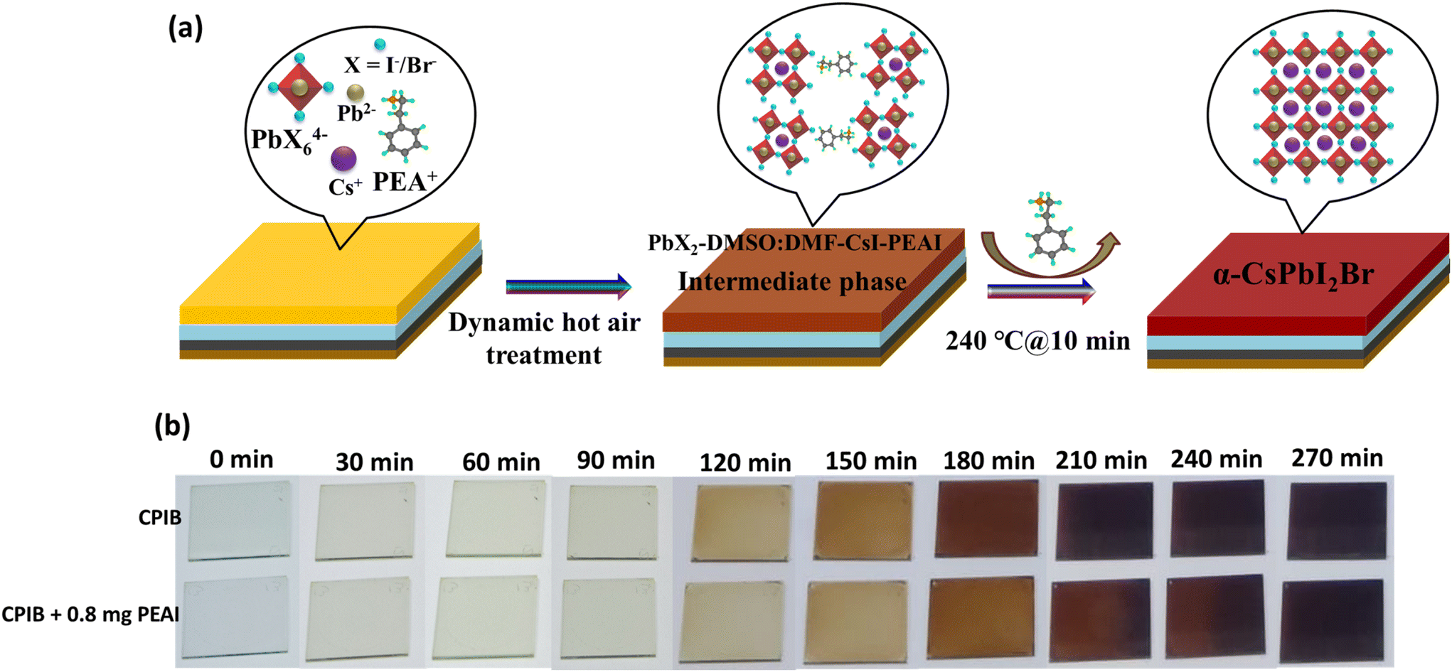 | ||
| Fig. 1 (a) Schematic representation of a possible mechanism and (b) digital photographs of CPIB and 0.8 mg PEAI-assisted perovskite films at various time intervals from 0 to 270 min during the crystallization process. | ||
Field-emission scanning electron microscopy measurements were conducted to investigate the microstructure of the prepared film to determine the influence of the PEAI additive on the CPIB perovskite film morphology. The micrographs of the CPIB and 0.4, 0.8, and 1.2 mg PEAI-treated perovskite films are depicted in Fig. 2(a–d), respectively. The CPIB perovskite film exhibits poor surface morphology with many pinholes, acting as non-radiation recombination centers that degrade device performance (Fig. 2a). With the addition of 0.4 mg of PEAI to the CPIB precursor solution, pinholes were reduced, and the surface morphology was improved; however, minor pinholes were still observed (Fig. 2b). When the PEAI concentration was increased from 0.4 to 0.8 mg, the pinholes were significantly suppressed, and the surface morphology became more uniform and densely packed (Fig. 2c). As the PEAI concentration was increased further to 1.2 mg, the film morphology was degraded (Fig. 2d). The excess concentration of PEAI can imbalance crystallization kinetics, resulting in unsatisfactory crystal growth which produces poor morphology of perovskite film. Moreover, a higher amount of PEAI would take more time to sublimate during the conversion of the intermediate phase (PbX2-DMSO:DMF-PEAI-CsI) into an α-CPIB active phase at 240 °C for 10 min, which might degrade the surface morphology of the film.
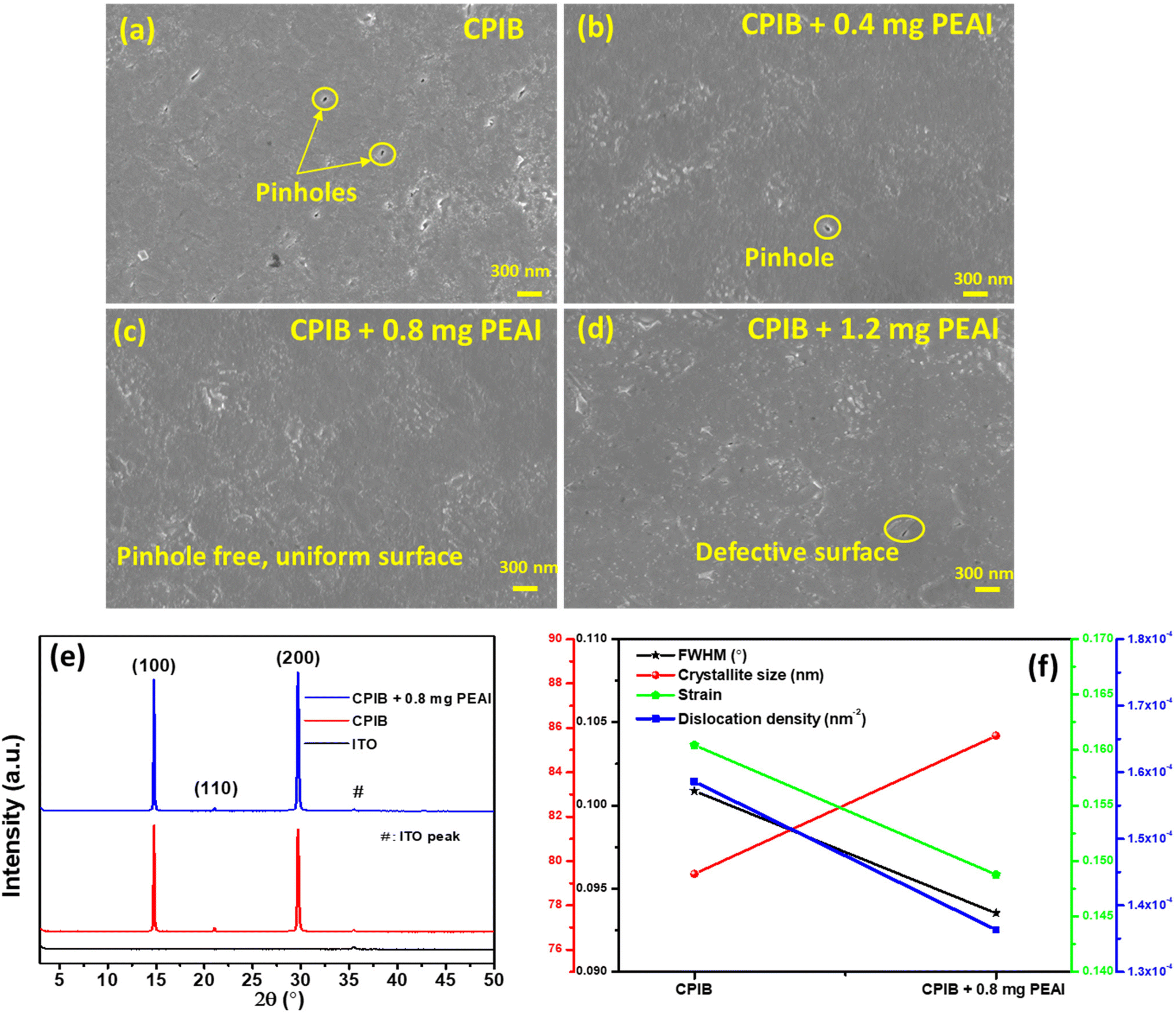 | ||
| Fig. 2 Field-emission scanning electron microscopy images of (a) CPIB, (b) 0.4 mg PEAI, (c) 0.8 mg PEAI, and (d) 1.2 mg PEAI-treated perovskite films. X-ray powder diffraction patterns of (e) CPIB and CPIB + 0.8 mg PEAI perovskite films. (f) The FWHM, average crystallite size, strain, and dislocation density of the extracted perovskite crystal corresponding to the CPIB and 0.8 mg PEAI-assisted perovskite films. | ||
The optimum concentration of PEAI controls the chemical reaction between CsI-PEAI-DMSO:DMF-PbX2 and retards the crystallization kinetics, resulting in Ostwald ripening, producing large grains, and reducing pinholes. The prolonged crystallization time with the PEAI additive is beneficial for improving film quality. The morphology results confirm that the pinholes were diminished with the PEAI additive. Thus, an optimized amount (0.8 mg) of PEAI produced high-quality perovskite film with a uniform surface.
The X-ray powder diffraction (XRD) patterns were recorded for the CPIB and CPIB + 0.8 mg PEAI perovskite films to evaluate the influence of the PEAI additive on the crystalline properties of CPIB, as depicted in Fig. 2(e). The CPIB film showed characteristic peaks at 14.78°, 21.01°, and 29.66°, which can be ascribed to the (100), (110), and (200) crystal planes, respectively, revealing the formation of an α-CPIB phase.8,39 After adding 0.8 mg of PEAI, no additional diffraction peak was found, confirming that the organic cation PEA+ could not form any secondary phases except for the α-CPIB phase.
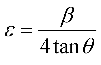
Moreover, after adding 0.8 mg of PEAI, high intense diffraction peaks were found at the same place of the 2θ value as depicted in the enlarged XRD spectra (Fig. S4(a and b)†). Notably, characteristic peaks ((100) and (200)) intensity values substantially increased with the addition of PEAI, indicating that the crystallinity of the perovskite film was enhanced. For a detailed analysis, we calculated the full width at half maximum (FWHM; β), the average crystallite size (D), strain (ε), and dislocation density (δ), as shown in Table S2 in the ESI.† The average crystal size was obtained using the Debye–Scherrer equation,40 as follows:
 | (1) |
 | (2) |
 | (3) |
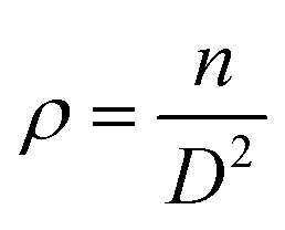
The dislocation density (ρ) was determined using the following equation:
 | (4) |
As depicted in Fig. 2(f), the value of β decreased, and the D value increased with the PEAI additive, suggesting that the crystallinity of CPIB film increased. Previous studies have demonstrated that the solution-processed CPIB film suffers from uncontrolled crystal growth, poor surface coverage, nonuniform morphology, and shallow trap states due to fast crystallization.39 Moreover, microstrain may occur due to the presence of various defects, such as dislocation, crystal imperfection, distortion, vacancies, and grain boundaries.41 The CPIB + 0.8 mg PEAI perovskite film exhibited lower strain and dislocation density values than the CPIB (Fig. 2(f)), which indicates a considerable reduction in defects.
To investigate the effect of the PEAI additive on optoelectronic properties, UV-visible patterns were recorded as shown in Fig. 3(a). Both perovskite films exhibit an almost similar optical bandgap (Eg) value of ∼1.88 eV (Fig. S5†), consistent with other reports.25,42,43 Interestingly, the CPIB + 0.8 mg PEAI perovskite film showed a higher absorption intensity than CPIB due to the suppression of the band-edge trap states,42 enhanced crystallinity, and improved film surface quality.23
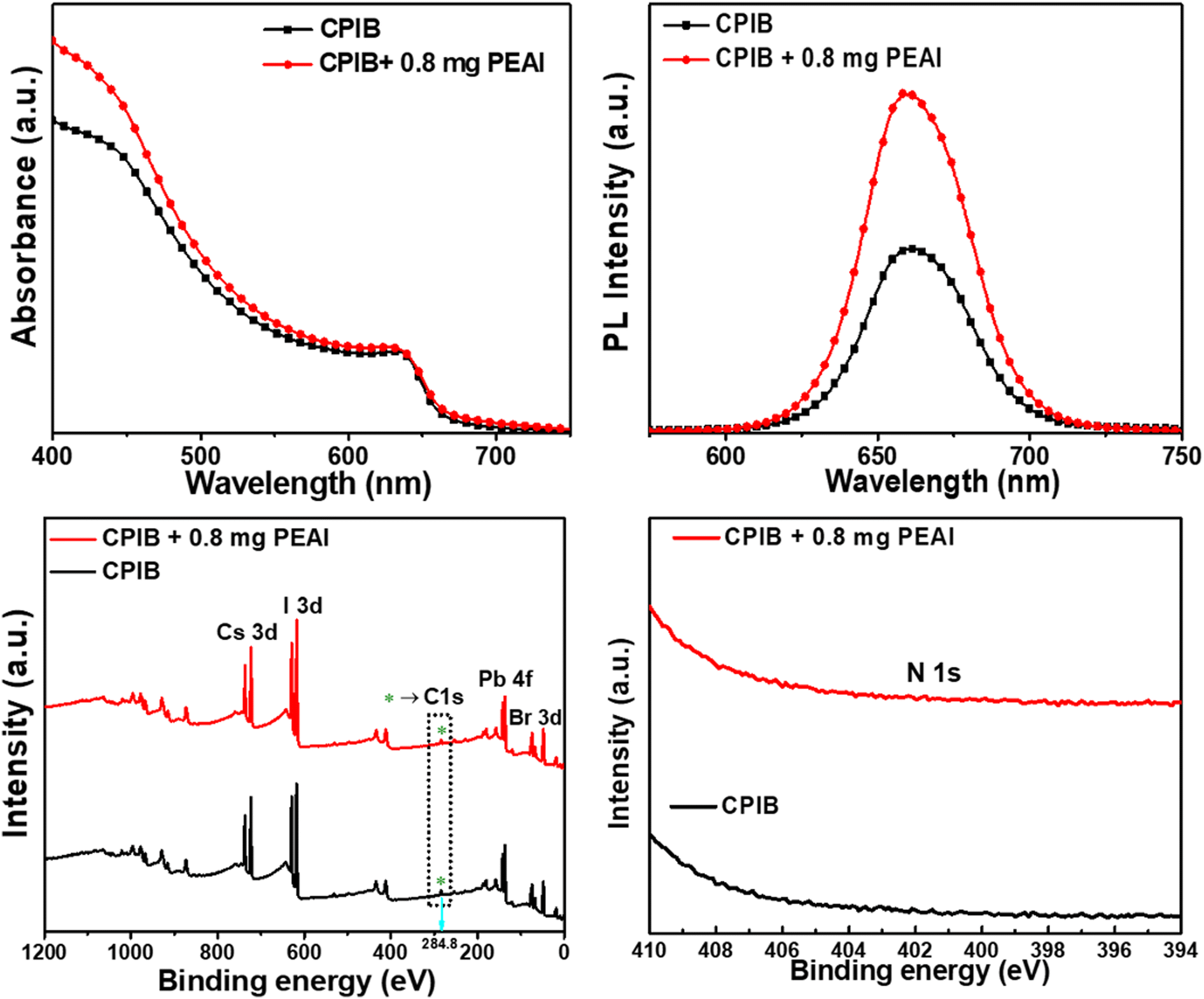 | ||
| Fig. 3 (a) Ultraviolet–visible absorption spectra, (b) PL patterns, (c) X-ray photoelectron spectroscopy survey scan, and (d) N 1s core-level spectrum for the CPIB and 0.8 mg PEAI-assisted perovskite films. | ||
To explore the photophysical properties of CPIB and CPIB + 0.8 mg PEAI perovskite films, steady-state photoluminescence (PL) spectra were measured as depicted in Fig. 3(b). The PEAI-treated film demonstrated high PL intensity compared to CPIB, indicating a significant suppression of nonradiative recombination centers.17,44 The increment in PL intensity revealed that charge trap states or defect densities were reduced due to the formation of the high-quality perovskite film,45,46 consistent with the field-emission scanning electron microscopy and XRD analyses.
The X-ray photoelectron spectroscopy (XPS) measurement was conducted to probe the elemental analysis corresponding to CPIB and CPIB + 0.8 mg PEAI perovskite films. The X-ray source energy (Al Kα: photon energy = 1486.6 eV, vacuum: ∼ 5 × 10⁻⁸ Torr) was used to acquire the XPS patterns. The complete XPS survey scan (Fig. 3(c)) shows the characteristic peaks corresponding to the core level of Cs 3d, I 3d, Pb 4f, and Br 3d for the CPIB and CPIB + 0.8 mg PEAI perovskite films. It is noteworthy to mention that we have not found any peak signal in the core level for the N 1s element in the CPIB + 0.8 mg PEAI perovskite (Fig. 3(d)), which reveals the complete sublimation of the PEA+ cation during high-temperature annealing (240 °C@10 min) and the results found in accordance with the above analysis. The adventitious carbon peak C 1s (as marked with a green color star symbol in Fig. 3(c)) was found in air-processed CPIB and 0.8 mg PEAI-assisted CPIB films. Various studies showed the XPS of pristine inorganic CsPbI2Br (CPIB)/CsPbBr3/CsPbIBr2 perovskites that consisted of the C 1s adventitious carbon peak,47–51 which might be due to the deposition of a tiny layer carbonaceous material on the surface when exposed to film under an air atmosphere.52–54 For instance, Liang et al. found the adventitious carbon C 1s peak in the XPS spectrum of inorganic CsPb0.9Sn0.1IBr2 perovskite film.47 The adventitious carbon C 1s peak was used to calibrate the XPS data.49
The high-resolution C 1s peak spectrum for CPIB and 0.8 mg PEAI CPIB films is provided in Fig. S6.† Comparatively, no additional peak related to the PEAI signature was found in the C 1s spectra of 0.8 mg PEAI assisted CPIB film, which also suggests the sublimation of organic cations (PEA+) during high-temperature processing under ambient air. Moreover, for CPIB and 0.8 mg PEAI-assisted perovskite films, we measured XPS spectrums with a surface scan as well as signals after surface etching using an Ar ion etching gun for 20 s and the obtained patterns are shown in Fig. S7.† The XPS patterns of CPIB and 0.8 mg PEAI-assisted perovskite films with the surface scan exhibited the C 1s adventitious carbon peak (as marked with the green color star symbol in Fig. S7†), while after surface treatment with the Ar ion etching gun for 20 s, the C 1s adventitious carbon peak was not detected in both perovskite films. Obviously, in the case of 0.8 mg PEAI-assisted CPIB film, no signal of the carbon peak was found in the XPS spectra of the etched surface, which also suggests the sublimation of the organic compound (PEA+) in high-temperature processing. Thus, we consider here that C 1s is an adventitious carbon peak as presented in the XPS surface scans of pristine CPIB and 0.8 mg PEAI-treated CPIB films.
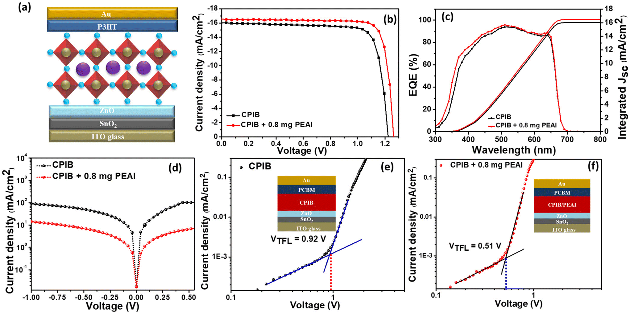
We further measured Fourier transform infrared (FTIR) spectra of PEAI, CPIB, and CPIB + 0.8 mg PEAI as shown in Fig. S8.† The peaks centered at 695, 746, 927, 1120 cm−1 are confirmed as the existence of a benzene ring in pristine PEAI.55 In addition, peaks observed at 1486 cm−1 and 1560 cm−1 can be assigned to N–H bending55 and aromatic C![[double bond, length as m-dash]](https://www.rsc.org/images/entities/char_e001.gif) C stretching vibration,56–58 respectively, from PEAI. Moreover, peaks around 2950–3100 cm−1 signify proton stretching vibration on the benzene ring from PEAI.58 The obtained FTIR spectrum of pristine CPIB is consistent with reported works.59,60 After the addition of 0.8 mg PEAI, it is noteworthy that no additional significant peak was found corresponding to the presence of the PEAI feature, which confirms the complete sublimation of PEAI during high-temperature annealing (240 °C@10 min) under an ambient atmosphere, and also consistent with XPS analysis. Devices were fabricated with the n-i-p structure (ITO/SnO2/ZnO/perovskite/P3HT/Au), as shown in the schematic diagram in Fig. 4(a) as well as the cross-section FESEM image of the cell (Fig. S9†), to analyze the effect of the PEAI additive on photovoltaic performance. The measured current density–voltage (J–V) curves of CPIB and various amounts (0.0, 0.4, 0.8, and 1.2 mg) of PEAI-based PSCs are depicted in Fig. 4(b) and Fig. S10.† The corresponding photovoltaic parameters are listed in Table 1 and Table S3.† Notably, photovoltaic performance improved with the addition of PEAI in the perovskite precursor. The CPIB device exhibited a power conversion efficiency (PCE) of 15.75% with a current density (Jsc) of 16.03 mA cm−2, an open-circuit voltage (Voc) of 1226 mV, and a fill factor (FF) of 80.15%. After adding 0.2 mg of PEAI, the device exhibited a PCE of 17.20%, Jsc of 16.43 mA cm−2, Voc of 1259 mV, and FF of 83.16%. When the PEAI concentration was increased to 0.8 mg, we observed further improvement in the PCE, Jsc, Voc, and FF as 17.40%, 16.47 mA cm−2, 1264 mV, and 83.56%, respectively. An improvement in photovoltaic parameters was attributed to the enhanced crystallinity, improved surface morphology, and reduced charge recombination with 0.8 mg of the PEAI additive. When we further increased the concentration to 1.2 mg, an opposite trend in photovoltaic parameters was observed (PCE = 17.20%, Jsc = 16.43 mA cm−2, Voc = 1259 mV, and FF = 83.16%), which might be due to imbalanced crystallization kinetics at an excess amount of PEAI that degraded the film quality (Fig. 2(d)).
C stretching vibration,56–58 respectively, from PEAI. Moreover, peaks around 2950–3100 cm−1 signify proton stretching vibration on the benzene ring from PEAI.58 The obtained FTIR spectrum of pristine CPIB is consistent with reported works.59,60 After the addition of 0.8 mg PEAI, it is noteworthy that no additional significant peak was found corresponding to the presence of the PEAI feature, which confirms the complete sublimation of PEAI during high-temperature annealing (240 °C@10 min) under an ambient atmosphere, and also consistent with XPS analysis. Devices were fabricated with the n-i-p structure (ITO/SnO2/ZnO/perovskite/P3HT/Au), as shown in the schematic diagram in Fig. 4(a) as well as the cross-section FESEM image of the cell (Fig. S9†), to analyze the effect of the PEAI additive on photovoltaic performance. The measured current density–voltage (J–V) curves of CPIB and various amounts (0.0, 0.4, 0.8, and 1.2 mg) of PEAI-based PSCs are depicted in Fig. 4(b) and Fig. S10.† The corresponding photovoltaic parameters are listed in Table 1 and Table S3.† Notably, photovoltaic performance improved with the addition of PEAI in the perovskite precursor. The CPIB device exhibited a power conversion efficiency (PCE) of 15.75% with a current density (Jsc) of 16.03 mA cm−2, an open-circuit voltage (Voc) of 1226 mV, and a fill factor (FF) of 80.15%. After adding 0.2 mg of PEAI, the device exhibited a PCE of 17.20%, Jsc of 16.43 mA cm−2, Voc of 1259 mV, and FF of 83.16%. When the PEAI concentration was increased to 0.8 mg, we observed further improvement in the PCE, Jsc, Voc, and FF as 17.40%, 16.47 mA cm−2, 1264 mV, and 83.56%, respectively. An improvement in photovoltaic parameters was attributed to the enhanced crystallinity, improved surface morphology, and reduced charge recombination with 0.8 mg of the PEAI additive. When we further increased the concentration to 1.2 mg, an opposite trend in photovoltaic parameters was observed (PCE = 17.20%, Jsc = 16.43 mA cm−2, Voc = 1259 mV, and FF = 83.16%), which might be due to imbalanced crystallization kinetics at an excess amount of PEAI that degraded the film quality (Fig. 2(d)).
 | ||
| Fig. 4 (a) Schematic representation of the device architecture, (b) current density–voltage curves, (c) EQE and Integrated Jsc patterns, and (d) dark current spectra of CPIB and 0.8 mg PEAI-based PSCs; space charge-limited current (SCLC) measurements for (e) the CPIB and (f) 0.8 mg PEAI-assisted PSCs. | ||
| Devices | J SC (mA cm−2) | V OC (mV) | FF (%) | PCE (%) |
|---|---|---|---|---|
| CPIB | 16.03 | 1226 | 80.15 | 15.75 |
| CPIB + 0.8 mg PEAI | 16.47 | 1264 | 83.56 | 17.40 |
These results suggest that the highest PCE of 17.40% was obtained with an optimum concentration of 0.8 mg of PEAI and is considered to be a champion device. Moreover, the external quantum efficiency (EQE) measurement was conducted to calculate the integrated Jsc for the CPIB and 0.8 mg PEAI additive-based PSCs. As shown in Fig. 4(c), the 0.8 mg PEAI-assisted PSC had higher absorption relative to the CPIB device because of the enhanced quality of the perovskite film. The integrated Jsc values of 16.01 mA cm−2 and 16.44 mA cm−2 were found, corresponding to the CPIB and 0.8 mg PEAI-assisted devices, respectively, which agree well with the obtained Jsc values from the J–V curves. The reproducibility was examined by fabricating 20 cells for both cases and the statistical analyses of the Jsc, Voc, FF, and PCE are demonstrated in Fig. S11.† The CPIB + 0.8 mg PEAI PSCs had a narrow distribution for all J–V parameters compared to the CPIB devices, indicating better repeatability with the PEAI additive. Moreover, with the systematic literature study, it can be concluded that champion PSC achieved an impressive PCE of 17.40%, which is almost similar to the record work (17.80%) in all-inorganic CPIB-based PSCs (Fig. S12†).
To explore the effect of the PEAI additive on the trap charge density, a space charge-limited current (SCLC) measurement was employed under dark conditions to quantitively examine trap states in perovskite films. We constructed electron-only devices with the architecture of ITO/SnO2/ZnO/perovskite/PC61BM/Au (Fig. S1† or inset in Fig. 4(d and e)) for the SCLC measurement. The dark J–V curves for the CPIB and CPIB + 0.8 mg PEAI electron-injecting devices are demonstrated in Fig. 4(d and e), respectively. The trap-filled limited voltage (VTFL) was extracted at the kink point, which indicates the transition of the curve from the ohmic region to the trap-filled limited region.1 The value of VTFL was calculated to be 0.92 and 0.51 V, corresponding to the CPIB and CPIB + 0.8 mg PEAI perovskite films, respectively. The trap-state density was estimated using the following equation:9,39
 | (5) |
Furthermore, dark J–V curves were measured for the CPIB and 0.8 mg PEAI-assisted device. As illustrated in Fig. 4(f), the CPIB + 0.8 mg PEAI PSC exhibited a lower dark current value than the CPIB device, indicating that the PEAI additive reduced the leakage current that originates from the presence of pinholes and grain boundaries.61 Thus, a smaller leakage current value for the 0.8 mg PEAI-based device suggests that pinholes and grain boundaries were considerably diminished in the perovskite film, according to the following formula:62
 | (6) |
The transient photovoltage (TPV) and transient photocurrent (TPC) decay spectra were measured to examine the charge carrier transport properties within PSCs. From the TPC results (Fig. 5(a)), the charge transport lifetime (τct) was calculated to be 1.14 and 0.88 μs for the CPIB and 0.8 mg PEAI-based PSCs, respectively. The rapid TPC decay was observed in the 0.8 mg PEAI-assisted device, which manifests faster extraction and transportation of photogenerated charge carriers.61 Better extraction and transport phenomena are attributed to the formation of a high-quality film with the 0.8 mg PEAI additive. Moreover, TPV decay curves showed charge carrier recombination lifetimes (τct) of 32.51 and 61.97 μs for the CPIB and CPIB + 0.8 mg PEAI devices, respectively (Fig. 5(b)). The increased charge carrier recombination lifetime revealed that nonradiative recombination remarkably reduced after adding 0.8 mg of PEAI.
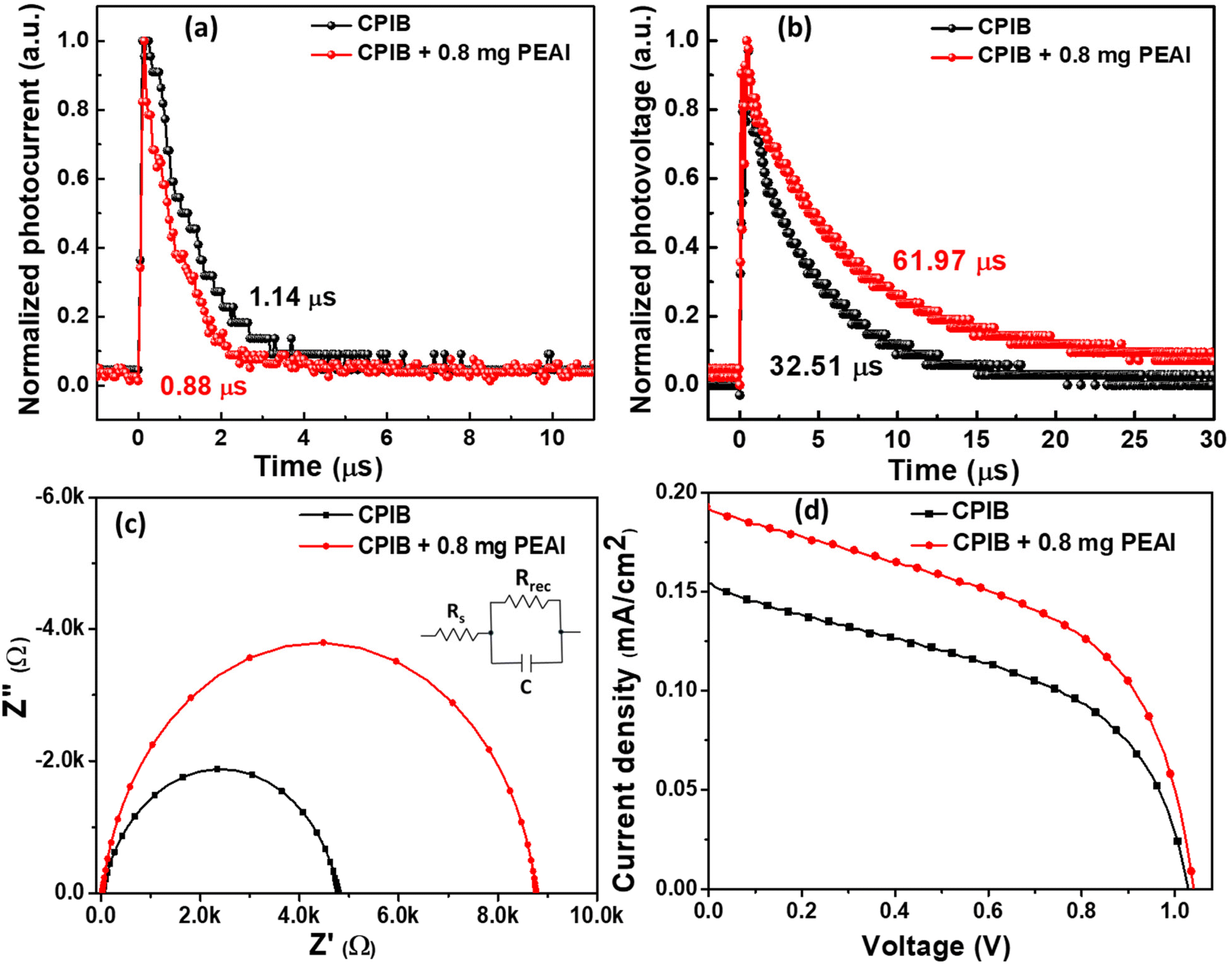 | ||
| Fig. 5 (a) Transient photocurrent, (b) transient photovoltage, (c) electrochemical impedance spectroscopy spectra, and (d) indoor current density–voltage curves under 1000 lux irradiation for CPIB and 0.8 mg PEAI CPIB-assisted PSCs. | ||
Furthermore, to investigate the charge carrier recombination dynamics of the CPIB and CPIB + 0.8 mg PEAI PSCs, the electrochemical impedance spectroscopy measurement was conducted under dark conditions with a frequency range from 100 Hz to 2 MHz and an applied bias voltage of 1.0 V. The electrochemical impedance spectroscopy curves were fitted using the Z-view software according to the equivalent circuit model containing series resistance (Rs), recombination resistance (Rrec), and chemical capacitance (C)63,64 as depicted in the inset of Fig. 5(c). Rs, the series resistance, is generally induced by various factors such as the ITO electrode interface, wires, and metal electrode interface.65,66Rs has a noticeable effect on the device fill factor (FF).67 For instance, the higher FF is linked with the lower series resistance.63 The recombination resistance (Rrec) indicates the recombination sites at the ETL/perovskite interface.68,69 The low frequency region of the Nyquist plot indicated the feature of Rrec.67 The recombination rate is strongly dependent on Rrec and it is inversely proportional to Rrec.67 The higher value of Rrec indicates that the charge recombination phenomena are significantly suppressed within the device.70,71
Thus, a minimum value of Rs and a higher value of Rrec are beneficial for obtaining the desired photovoltaic performance of PSCs. The values of Rs and Rrec were extracted from Nyquist plots corresponding to the intercept of the Z′(Ω) axis at a high frequency and diameter of the semicircle, respectively.9,42 The Nyquist plots are illustrated in Fig. 5(c) and the fitting parameters are shown in Table S4.† The 0.8 mg PEAI additive device exhibited a lower value of series resistance (26 Ω) than the CPIB PSC (29 Ω). The reduction in the series resistance indicates more effective charge transport phenomena, which is favorable to the FF improvement.72,73 Moreover, the 0.8 mg PEAI-based PSC shows a larger recombination resistance value (8745 Ω) in the low-frequency region relative to the CPIB device (4759 Ω), indicating that bulk and surface nonradiative recombination were significantly suppressed,42 which agree well with the SCLC and TPV results. Therefore, the 0.8 mg PEAI-treated device exhibits efficient charge transportation, reduced recombination, and minimal energy loss, leading to a higher Voc and FF.
Electricity generation under dim lighting (indoor environment) is an essential application of PSCs in indoor-operated photovoltaic technologies. Thus, we examined indoor photovoltaic performance under white light-emitting diode (LED, 3200 K) irradiation of 1000 lux, a typical daily-life lighting condition. The power density of the white LED light was 382.0 μW cm−2 at 1000 lux in this study. The measured J–V curves of the CPIB and CPIB + 0.8 mg PEAI PSCs are presented in Fig. 5(d), and the related parameters are listed in Table 2. The CPIB device exhibits a power density of 75.19 μW cm−2 with a PCE of 19.68%, Jsc of 154 μA cm−2, Voc of 1.029 V, and FF of 47.45%. In the case of the 0.8 mg PEAI additive, the PSC demonstrated a high PCE of 26.73%, Jsc of 192 μA cm−2, Voc of 1.041 V, FF of 51.10%, and the corresponding power density of 102.13 μW cm−2. It is worth noting that indoor photovoltaic parameters significantly improved with the 0.8 mg PEAI additive. As compared to 1-sun performance, the higher PCE of the device can be achieved under indoor (LED) lighting conditions. This is attributed to the narrower spectral band of the white LED, decreasing the thermal and transparency losses.74,75
| Devices | J SC (μA cm−2) | V OC (mV) | FF (%) | P indoor (μW cm−2) | PCE (%) |
|---|---|---|---|---|---|
| CPIB | 154 | 1029 | 47.45 | 75.19 | 19.68 |
| CPIB + 0.8 mg PEAI | 192 | 1041 | 51.10 | 102.13 | 26.73 |
The highly efficient and stable CPIB PSCs under indoor light conditions will promote the advanced development of portable electronic devices. As shown in Fig. S13(a and b†), it can be used in switching applications, and also enable to power various portable electronic devices such as LoRa Backscatters, radio-frequency identification (RFID), wristwatches, etc.76–78 From the commercialization aspect, we designed electronic circuits (Fig. 6(a and b)) by employing a 0.8 mg PEAI additive-based PSC to produce a switching function under LED light (3200 K) irradiation at 1000 lux. The ANA618 integrated circuit (IC) was used to design the electronic circuit for producing the switching output function. The schematic of ANA618 IC and each corresponding pin description is shown in Fig. S14 (ESI†). The IC ANA618 is specially designed to drive the load such as that acting as an LED, small power-based motors, etc. using a low power supply. The internal circuitry of IC ANA618 consists of oscillators, transistors, LED driver circuits, etc. The ANA618 IC needs only one inductor as an external component to develop a boost power supply with 85 to 90%. It has low power consumption and lower minimum operating voltage and is convenient, safe, and environmentally friendly.
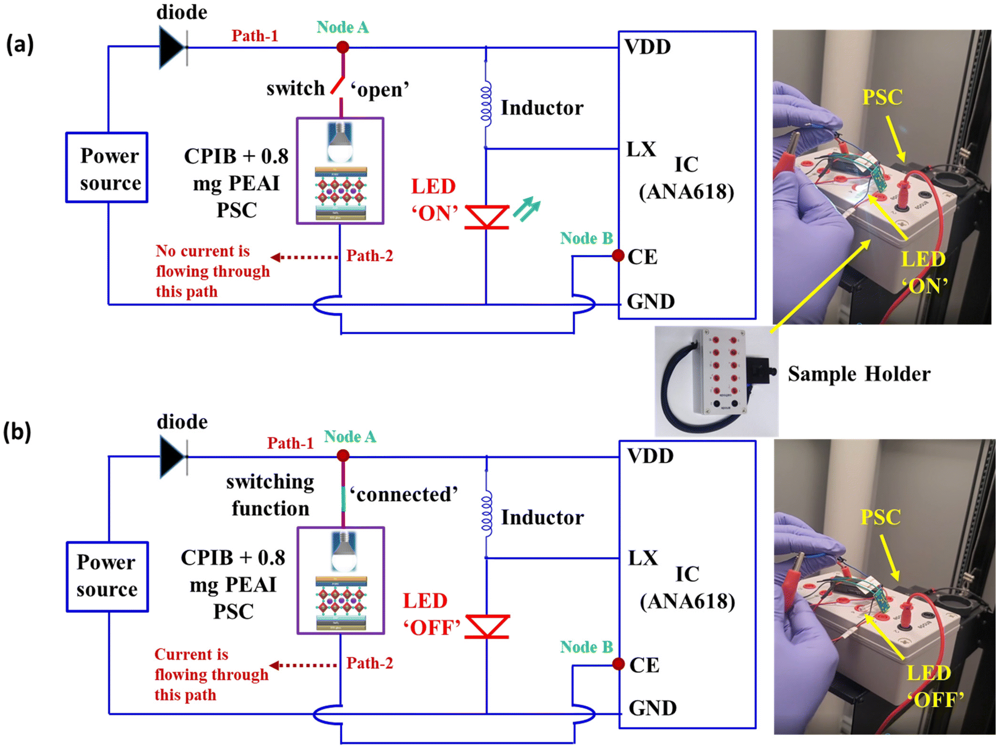 | ||
| Fig. 6 (a) A circuit diagram for the light-emitting diode (LED) “on state” with a digital photograph, and (b) a circuit diagram for the LED “off state” with a digital photograph; inset: the digital photograph with the sample holder. | ||
As depicted in Fig. 6(a and b), when the indoor PSC is not connected, the LED is in the “on state”, whereas when the indoor PSC is connected to the circuit, the LED is in the “off state” (see digital photographs). In addition, a demonstration of LED “ON” and “OFF” implementation using the CPIB + 0.8 mg PEAI PSC is shown in the ESI video,† which clearly suggests that the 0.8 mg PEAI-based PSC under lighting conditions plays a key role in the output switching function of the electronic circuit. The working mechanism of the designed circuit is given below:
(1) From Fig. 6(a), when PSC is not connected, IC ANA618 acts as an LED driver and glows the LED using an input power source. Noticeably, in this case, no current is flowing through path-2 (Node A–Node B) as the circuit is open and the chip enable (CE) pin is not activated.
(2) When PSC is connected under indoor light illumination (Fig. 6(b)), the current is flowing through the path-2 (Node A–Node B) and the chip enable (CE) pin is activated, which triggers the LX pin (switch) to halt the oscillator output (LED driver), and hence LED turned-off.
The PSC under lighting conditions acts as a voltage source and provides the desired current flow between Node A and Node B (CE pin) (Fig. 6(b)). Thus, PSC plays a vital role in activating the CE pin that triggers the output of the LX pin, and the LED is in the OFF state as shown in Fig. 6(b). Therefore, we can produce the switching function by employing an efficient PSC under indoor lighting conditions using an ANA618 IC controller. This type of switching can be used to power smart curtains that are automatically opened or closed according to indoor light conditions. From technological advancement aspects and designing smart rooms, such practical applicability of these devices must be explored more.
An aging test was performed on the CPIB and CPIB + 0.8 mg PEAI perovskite films under ambient conditions (relative humidity: ∼45% and temperature: ∼22.8 °C) to examine the air stability of perovskite films. The film degradation was tracked at different time intervals and digital photographs were captured, as shown in Fig. 7(a). The CPIB film showed rapid decomposition compared with the CPIB + 0.8 mg PEAI perovskite film after aging for 120 min. As a result, the optimized PEAI additive improved the ambient stability, which could be ascribed to better crystallization, reduced defect density, and favorable morphology.
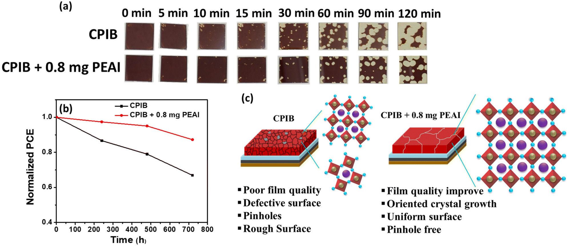 | ||
| Fig. 7 (a) Digital images of the CPIB and 0.8 mg PEAI-assisted perovskite films at time intervals under ambient air aging conditions (relative humidity: ∼45% and temperature: ∼22.8 °C) (b) long-term thermal stability for CPIB and 0.8 mg PEAI-treated PSCs in a dry box and (c) schematic representation of the benefits of the PEAI additive. | ||
Furthermore, we monitored the thermal stability of PSCs at 85 °C in a dry box (relative humidity range: 10%–14% and temperature range: 26–31 °C) over 720 h without encapsulation. As presented in Fig. 7(b), the 0.8 mg PEAI treated device showed an ∼87.25% retention of the initial PCE, whereas the CPIB device maintained ∼66.90% of the original PCE after aging at 85 °C in a dry box for 720 h. The optimized device exhibited superior thermal stability, and the PCE decreased by only ∼12.75% of its initial value. Thus, the PEAI additive stabilizes PSC performance under thermal stress due to improved film quality. Based on these positive findings, PEAI plays a critical role in improving device performance and thermal stability and benefits in several ways, such as reduced pinholes, enhanced crystallinity and uniformity, and dense morphology, as illustrated in the schematic diagram (Fig. 7(c)). We believe that this additive-based strategy could open new promising methods for further developing efficient and stable all-inorganic PSCs.
Conclusions
In summary, we fabricated a high-quality CPIB film with good crystallinity, pinhole-free, uniform, and compact morphology using an additive strategy. It is worth noting that a PEAI additive retards the crystallization kinetics, resulting in reduced pinholes, well-ordered crystal growth, increased crystallinity, decreased trap density states, and improved overall film surface morphology. These favorable properties suggest that nonradiative recombination is remarkably suppressed with the PEAI additive. As a result, the optimized PEAI concentration (0.8 mg) PSC had a high PCE of 17.40% relative to the CPIB PSC (15.75%). The 0.8 mg PEAI-assisted device exhibited superior thermal stability in a dry box at 85 °C over 720 h by maintaining ∼87.25% of the initial PCE value, whereas the CPIB device retained ∼66.90% of the original PCE. Moreover, the optimized device achieved an impressive PCE of 26.73% under an LED light source (3200 K, 1000 lux). In addition, the switching function indicated the practical applicability of the champion device. Thus, these findings suggest that an additive-based approach opens up a promising avenue to produce a high-quality α-CPIB film for efficient and stable PSC development under indoor/outdoor lighting conditions.Author contributions
Jitendra Bahadur: conceptualization, methodology, investigation, validation, data curation, visualization, formal analysis, and writing – original draft. Jun Ryu: data curation, visualization, characterization, and formal analysis. Padmini Pandey: data curation, investigation, validation, visualization, formal analysis, and review. SungWon Cho: data curation, visualization, and formal analysis. Jung Sang Cho: review & editing, conceptualization, and supervision. Dong-Won Kang: writing – review & editing, conceptualization, supervision, project administration, and funding acquisition.Conflicts of interest
There are no conflicts to declare.Acknowledgements
This work was supported by the National Research Foundation of Korea (NRF) grant funded by the Korean government (MSIT) (NRF – 2021R1A2C4002045, 2021R1A4A2001687, 2021K2A9A2A08000082 and 2022H1D3A2A01096254).References
- W. Tang, Y. Chen, J. Yang, R. Yuan, Y. Lv, Q. Ma, Y. Wu, P. Zhang and W.-H. Zhang, J. Power Sources, 2021, 482, 228965 CrossRef CAS.
- H. Wang, H. Bian, Z. Jin, H. Zhang, L. Liang, J. Wen, Q. Wang, L. Ding and S. F. Liu, Chem. Mater., 2019, 31, 6231–6238 CrossRef CAS.
- Y.-H. Kye, C.-J. Yu, C.-H. Kim, Y.-S. Kim and U.-G. Jong, J. Phys. Chem. C, 2021, 125, 13195–13211 CrossRef CAS.
- J. Han, K. Kim, J. S. Nam, S. J. Hong, E. J. Choi, D. Kim, I. Chung, H. S. Lin, T. D. Kim and M. S. Strano, Adv. Energy Mater., 2021, 11, 2101221 CrossRef CAS.
- A. Kojima, K. Teshima, Y. Shirai and T. Miyasaka, J. Am. Chem. Soc., 2009, 131, 6050–6051 CrossRef CAS PubMed.
- H. Min, D. Y. Lee, J. Kim, G. Kim, K. S. Lee, J. Kim, M. J. Paik, Y. K. Kim, K. S. Kim and M. G. Kim, Nature, 2021, 598, 444–450 CrossRef CAS PubMed.
- D. J. Kubicki, D. Prochowicz, A. Hofstetter, M. Saski, P. Yadav, D. Bi, N. Pellet, J. Lewinski, S. M. Zakeeruddin and M. Grätzel, J. Am. Chem. Soc., 2018, 140, 3345–3351 CrossRef CAS PubMed.
- J. K. Nam, M. S. Jung, S. U. Chai, Y. J. Choi, D. Kim and J. H. Park, J. Phys. Chem. Lett., 2017, 8, 2936–2940 CrossRef CAS PubMed.
- S. Fu, J. Wang, X. Liu, H. Yuan, Z. Xu, Y. Long, J. Zhang, L. Huang, Z. Hu and Y. Zhu, Chem. Eng. J., 2021, 422, 130572 CrossRef CAS.
- C. Liu, Y. Yang, C. Zhang, S. Wu, L. Wei, F. Guo, G. M. Arumugam, J. Hu, X. Liu and J. Lin, Adv. Mater., 2020, 32, 1907361 CrossRef CAS PubMed.
- Q. Zeng, X. Zhang, C. Liu, T. Feng, Z. Chen, W. Zhang, W. Zheng, H. Zhang and B. Yang, Sol. RRL, 2019, 3, 1800239 CrossRef.
- W. Chen, H. Chen, G. Xu, R. Xue, S. Wang, Y. Li and Y. Li, Joule, 2019, 3, 191–204 CrossRef CAS.
- K. Jiang, J. Wang, F. Wu, Q. Xue, Q. Yao, J. Zhang, Y. Chen, G. Zhang, Z. Zhu and H. Yan, Adv. Mater., 2020, 32, 1908011 CrossRef CAS PubMed.
- M. K. Mohanta, A. Kishore and A. De Sarkar, ACS Appl. Mater. Interfaces, 2021, 13, 40872–40879 CrossRef CAS PubMed.
- H. Aqoma, I. F. Imran, F. T. A. Wibowo, N. V. Krishna, W. Lee, A. K. Sarker, D. Y. Ryu and S. Y. Jang, Adv. Energy Mater., 2020, 10, 2001188 CrossRef CAS.
- H. Sun, J. Zhang, X. Gan, L. Yu, H. Yuan, M. Shang, C. Lu, D. Hou, Z. Hu and Y. Zhu, Adv. Energy Mater., 2019, 9, 1900896 CrossRef.
- H. Zhao, Y. Han, Z. Xu, C. Duan, S. Yang, S. Yuan, Z. Yang, Z. Liu and S. Liu, Adv. Energy Mater., 2019, 9, 1902279 CrossRef CAS.
- K.-L. Wang, R. Wang, Z.-K. Wang, M. Li, Y. Zhang, H. Ma, L.-S. Liao and Y. Yang, Nano Lett., 2019, 19, 5176–5184 CrossRef CAS PubMed.
- S.-C. Chen, D. Wang and Q. Zheng, Sol. RRL, 2020, 4, 2000321 CrossRef CAS.
- S. S. Mali, J. V. Patil, J. A. Steele, S. R. Rondiya, N. Y. Dzade and C. K. Hong, ACS Energy Lett., 2021, 6, 778–788 CrossRef CAS PubMed.
- L. Yu, T. Guo, H. Yuan, Z. Zhang, Z. Deng, R. Zhao, M. Zheng, J. Zhang, W. Xu and X. Liu, Chem. Eng. J., 2021, 420, 129931 CrossRef CAS.
- Y. Wang, X. Liu, T. Zhang, X. Wang, M. Kan, J. Shi and Y. Zhao, Angew. Chem., 2019, 131, 16844–16849 CrossRef.
- J. V. Patil, S. S. Mali and C. K. Hong, ACS Appl. Mater. Interfaces, 2022, 14, 25576–25583 CrossRef CAS PubMed.
- J. V. Patil, S. S. Mali and C. K. Hong, Mater. Today Chem., 2022, 26, 101118 CrossRef CAS.
- K. S. Kim, I. S. Jin, S. H. Park, S. J. Lim and J. W. Jung, ACS Appl. Mater. Interfaces, 2020, 12, 36228–36236 CrossRef CAS PubMed.
- I. S. Jin, B. Parida and J. W. Jung, J. Mater. Sci. Technol., 2022, 102, 224–231 CrossRef.
- K. Kim, Z. Wu, J. Han, Y. Ma, S. Lee, S. K. Jung, J. W. Lee, H. Y. Woo and I. Jeon, Adv. Energy Mater., 2022, 12, 2200877 CrossRef CAS.
- M. Tai, Y. Zhou, X. Yin, J. Han, Q. Zhang, Y. Zhou and H. Lin, J. Mater. Chem. A, 2019, 7, 22675–22682 RSC.
- H. Wang, H. Bian, Z. Jin, L. Liang, D. Bai, Q. Wang and S. F. Liu, Sol. RRL, 2018, 2, 1800216 CrossRef.
- G. Wu, R. Liang, M. Ge, G. Sun, Y. Zhang and G. Xing, Adv. Mater., 2022, 34, 2105635 CrossRef CAS PubMed.
- J. Wang, S. Fu, X. Liu, H. Yuan, Z. Xu, C. Wang, J. Zhang, L. Huang, Z. Hu and Y. Zhu, J. Alloys Compd., 2022, 891, 161971 CrossRef CAS.
- X.-N. Huo, K.-X. Wang, R. Yin, W.-W. Sun, Y.-S. Sun, Y.-K. Gao, T.-T. You and P.-G. Yin, Sol. Energy Mater. Sol. Cells, 2022, 247, 111963 CrossRef CAS.
- L. Yan, Q. Xue, M. Liu, Z. Zhu, J. Tian, Z. Li, Z. Chen, Z. Chen, H. Yan and H. L. Yip, Adv. Mater., 2018, 30, 1802509 CrossRef PubMed.
- U. Khan, T. Iqbal, M. Khan and R. Wu, Sol. Energy, 2021, 223, 346–350 CrossRef CAS.
- S. S. Mali, J. V. Patil and C. K. Hong, Nano Lett., 2019, 19, 6213–6220 CrossRef CAS PubMed.
- S. S. Mali, J. V. Patil, P. S. Shinde, G. de Miguel and C. K. Hong, Matter, 2021, 4, 635–653 CrossRef CAS.
- J. V. Patil, S. S. Mali and C. K. Hong, ACS Sustainable Chem. Eng., 2020, 8, 16364–16371 CrossRef CAS.
- S. S. Mali, J. V. Patil and C. K. Hong, Adv. Energy Mater., 2020, 10, 1902708 CrossRef CAS.
- H. Li, X. Hao, B. Chang, Z. Li, L. Wang, L. Pan, X. Chen and L. Yin, ACS Appl. Mater. Interfaces, 2021, 13, 40489–40501 CrossRef CAS PubMed.
- S. Khalid, M. A. Malik, D. J. Lewis, P. Kevin, E. Ahmed, Y. Khan and P. O'Brien, J. Mater. Chem. C, 2015, 3, 12068–12076 RSC.
- I. Robinson and R. Harder, Nat. Mater., 2009, 8, 291–298 CrossRef CAS PubMed.
- S. Fu, W. Zhang, X. Li, L. Wan, Y. Wu, L. Chen, X. Liu and J. Fang, ACS Energy Lett., 2020, 5, 676–684 CrossRef CAS.
- X. Liu, H. Lian, Z. Zhou, C. Zou, J. Xie, F. Zhang, H. Yuan, S. Yang, Y. Hou and H. G. Yang, Adv. Energy Mater., 2022, 12, 2103933 CrossRef CAS.
- S. Yang, H. Zhao, M. Wu, S. Yuan, Y. Han, Z. Liu, K. Guo, S. F. Liu, S. Yang and H. Zhao, Sol. Energy Mater. Sol. Cells, 2019, 201, 110052 CrossRef CAS.
- Y. Guo, W. Sato, K. Shoyama, H. Halim, Y. Itabashi, R. Shang and E. Nakamura, J. Am. Chem. Soc., 2017, 139, 9598–9604 CrossRef CAS PubMed.
- L. Zuo, Z. Gu, T. Ye, W. Fu, G. Wu, H. Li and H. Chen, J. Am. Chem. Soc., 2015, 137, 2674–2679 CrossRef CAS PubMed.
- J. Liang, P. Zhao, C. Wang, Y. Wang, Y. Hu, G. Zhu, L. Ma, J. Liu and Z. Jin, J. Am. Chem. Soc., 2017, 139, 14009–14012 CrossRef CAS PubMed.
- Y. Long, K. Liu, Y. Zhang and W. Li, Molecules, 2021, 26, 3398 CrossRef CAS PubMed.
- Y. Liu, T. Xiang, B. Zhang, J. Wang, X. Yu, Y. Xiao, J. Xiao, Z. Ku and Y. Peng, ACS Appl. Energy Mater., 2022, 5, 8049–8056 CrossRef CAS.
- K. Fatima, M. I. Haider, A. Bashir, S. Qamar, A. A. Qureshi, Z. Akhter and M. Sultan, Phys. E, 2022, 142, 115265 CrossRef CAS.
- Y. Zhang, Y. Huang, C. Zhou, Y. Xu, J. Zhong and H. Mao, Vacuum, 2022, 202, 111219 CrossRef CAS.
- G. Greczynski and L. Hultman, ChemPhysChem, 2017, 18, 1507–1512 CrossRef CAS PubMed.
- T. L. Barr and S. Seal, J. Vac. Sci. Technol., A, 1995, 13, 1239–1246 CrossRef CAS.
- H. Piao and N. S. Mcintyre, Surf. Interface Anal., 2002, 33, 591–594 CrossRef CAS.
- K. Wang, Z. Jin, L. Liang, H. Bian, D. Bai, H. Wang, J. Zhang, Q. Wang and S. Liu, Nat. Commun., 2018, 9, 1–8 CrossRef PubMed.
- P. Chen, Y. Bai, S. Wang, M. Lyu, J. H. Yun and L. Wang, Adv. Funct. Mater., 2018, 28, 1706923 CrossRef.
- F. Zhang, Q. Huang, J. Song, Y. Zhang, C. Ding, F. Liu, D. Liu, X. Li, H. Yasuda and K. Yoshida, Sol. RRL, 2020, 4, 1900243 CrossRef CAS.
- N. Li, Z. Zhu, Q. Dong, J. Li, Z. Yang, C. C. Chueh, A. K. Y. Jen and L. Wang, Adv. Mater. Interfaces, 2017, 4, 1700598 CrossRef.
- J. Wang, L. Chen, Z. Qian, G. Ren, J. Wu and H. Zhang, J. Mater. Chem. A, 2020, 8, 25336–25344 RSC.
- X. Yang, J. Han, W. Ruan, Y. Hu, Z. He, X. Jia, S. Zhang and D. Wang, Chin. Chem. Lett., 2022, 33, 1425–1429 CrossRef CAS.
- Z. Zeng, J. Zhang, X. Gan, H. Sun, M. Shang, D. Hou, C. Lu, R. Chen, Y. Zhu and L. Han, Adv. Energy Mater., 2018, 8, 1801050 CrossRef.
- H. Li and L. Yin, Sol. RRL, 2020, 4, 2000268 CrossRef CAS.
- Z. Liu, S. Wu, X. Yang, Y. Zhou, J. Jin, J. Sun, L. Zhao and S. Wang, Nanoscale Adv., 2020, 2, 5396–5402 RSC.
- J. V. Patil, S. S. Mali and C. K. Hong, Sol. RRL, 2020, 4, 2000164 CrossRef CAS.
- G. Niu, W. Li, F. Meng, L. Wang, H. Dong and Y. Qiu, J. Mater. Chem. A, 2014, 2, 705–710 RSC.
- A. Guerrero, J. Bisquert and G. Garcia-Belmonte, Chem. Rev., 2021, 121, 14430–14484 CrossRef CAS PubMed.
- E. J. Juarez-Perez, M. Wuβler, F. Fabregat-Santiago, K. Lakus-Wollny, E. Mankel, T. Mayer, W. Jaegermann and I. Mora-Sero, J. Phys. Chem. Lett., 2014, 5, 680–685 CrossRef CAS PubMed.
- Y. Yang, J. Song, Y. Zhao, L. Zhu, X. Gu, Y. Gu, M. Che and Y. Qiang, J. Alloys Compd., 2016, 684, 84–90 CrossRef CAS.
- J. Song, S. Li, Y. Zhao, J. Yuan, Y. Zhu, Y. Fang, L. Zhu, X. Gu and Y. Qiang, J. Alloys Compd., 2017, 694, 1232–1238 CrossRef CAS.
- I. Jeong, Y. H. Park, S. Bae, M. Park, H. Jeong, P. Lee and M. J. Ko, ACS Appl. Mater. Interfaces, 2017, 9, 36865–36874 CrossRef CAS PubMed.
- H. Dhifaoui, N. H. Hemasiri, W. Aloui, A. Bouazizi, S. Kazim and S. Ahmad, Adv. Mater. Interfaces, 2021, 8, 2101002 CrossRef CAS.
- G. Sathiyan, A. A. Syed, C. Chen, C. Wu, L. Tao, X. Ding, Y. Miao, G. Li, M. Cheng and L. Ding, Nano Energy, 2020, 72, 104673 CrossRef CAS.
- X. Liu, Y. Cheng, C. Liu, T. Zhang, N. Zhang, S. Zhang, J. Chen, Q. Xu, J. Ouyang and H. Gong, Energy Environ. Sci., 2019, 12, 1622–1633 RSC.
- K.-L. Wang, Y.-H. Zhou, Y.-H. Lou and Z.-K. Wang, Chem. Sci., 2021, 12, 11936–11954 RSC.
- A. S. Teran, J. Wong, W. Lim, G. Kim, Y. Lee, D. Blaauw and J. D. Phillips, IEEE Trans. Electron Devices, 2015, 62, 2170–2175 CAS.
- V. Pecunia, L. G. Occhipinti and R. L. Hoye, Adv. Energy Mater., 2021, 11, 2100698 CrossRef CAS.
- V. Annapureddy, H. Palneedi, G.-T. Hwang, M. Peddigari, D.-Y. Jeong, W.-H. Yoon, K.-H. Kim and J. Ryu, Sustainable Energy Fuels, 2017, 1, 2039–2052 RSC.
- M. T. Todaro, F. Guido, L. Algieri, V. M. Mastronardi, D. Desmaële, G. Epifani and M. De Vittorio, IEEE Trans. Nanotechnol., 2018, 17, 220–230 CAS.
Footnote |
| † Electronic supplementary information (ESI) available. See DOI: https://doi.org/10.1039/d2nr06230e |
| This journal is © The Royal Society of Chemistry 2023 |