 Open Access Article
 This Open Access Article is licensed under a Creative Commons Attribution-Non Commercial 3.0 Unported Licence
Electrochemical characterization of individual oil micro-droplets by high-frequency nanocapacitor array imaging†
Christophe
Renault
 ab,
Cecilia
Laborde
a,
Andrea
Cossettini
cd,
Luca
Selmi
e,
Frans
Widdershoven
f and
Serge G.
Lemay
*a
ab,
Cecilia
Laborde
a,
Andrea
Cossettini
cd,
Luca
Selmi
e,
Frans
Widdershoven
f and
Serge G.
Lemay
*a
aMESA+ Institute for Nanotechnology, University of Twente, P.O. Box 217, 7500 AE Enschede, The Netherlands. E-mail: s.g.lemay@utwente.nl
bLaboratoire de Physique de la Matière Condensée, Ecole Polytechnique, CNRS, IP Paris, Route de Saclay, Palaiseau, 91128, France
cIntegrated Systems Laboratory, ETH Zürich, Gloriastrasse 35, 8092 Zürich, Switzerland
dDPIA, Università degli Studi di Udine, via delle Scienze 206, 33100 Udine, Italy
eDIEF, University of Modena and Reggio Emilia, Via Vivarelli 10, Modena, 41125, Italy
fNXP Semiconductors, Technology & Operations/CTO office, High Tech Campus 46, Eindhoven 5656 AE, The Netherlands
First published on 19th August 2021
Abstract
CMOS-based nanocapacitor arrays allow local probing of the impedance of an electrolyte in real time and with sub-micron spatial resolution. Here we report on the physico-chemical characterization of individual microdroplets of oil in a continuous water phase using this new tool. We monitor the sedimentation and wetting dynamics of individual droplets, estimate their volume and infer their composition based on their dielectric constant. From measurements before and after wetting of the surface, we also attempt to estimate the contact angle of individual micron-sized droplets. These measurements illustrate the capabilities and versatility of nanocapacitor array technology.
Introduction
Electrochemical impedance spectroscopy (EIS) is a powerful and flexible technique for probing electrochemical processes at the surface and in the vicinity of an electrode. The nature of the information that is probed depends on the frequency f at which a measurement is performed. This is characterized by the frequency f1 = 1/2πReCe, where Ce and Re are the electrical double layer (EDL) capacitance and the solution access resistance of the electrode, respectively. For f < f1, the measured response is dominated by Ce and the technique is primarily sensitive to the structure of the EDL. For f > f1, the response is instead dominated by Re, and in this case the composition of the solution away from the electrode is probed. Since the electric field falls off slowly with distance r from the electrode, the interaction with the sample is long-range and extends many times the radius of a disk electrode, re, into the solution. EIS measurements at a nanoelectrode thus provide a very local probe of either the properties of a solid–liquid interface or of an electrolyte in the vicinity of the electrode, depending on the choice of frequency. In practice, however, these measurements are technically very challenging to implement for a nanoelectrode for two main reasons:(1) The desired signal is easily obscured by parasitic current pathways. The capacitance of a nanoelectrode in aqueous media is of the order Ce ∼ 10−15 F. In conventional measurements based on standard EIS instrumentation, this is dwarfed by the capacitance of the interconnects to the electrode. As a rough illustration, the capacitance of a coaxial cable is ∼10−12 F cm−1, so even 1 cm of cable causes a background current that is 1000 times larger than the target signal. A nanoelectrode thus contributes only a very minor fraction of the total current flowing through the system, making it difficult to distinguish its contribution from the large background current.
(2) Reaching the regime f > f1 becomes increasingly difficult with decreasing electrode size. The parallel-plate component of the electrode’s EDL capacitance scales with electrode radius as Ce ∝ re2 while the spreading access resistance scales as Re ∝ re−1, hence f1 ∝ re−1. Shrinking the electrode size from re = 10 μm to 10 nm thus requires accessing 1000 times higher frequencies in order to probe the solution beyond the EDL.
Two main approaches have been used to overcome these challenges. Frequency mixing methods employ an active material (a field-effect transistor) as the electrode. The nonlinear response of the current through the transistor to the EDL potential allows applying high-frequency voltages yet reading out the resulting response at much lower frequencies via heterodyne methods.1 In a more direct approach, we have previously reported a platform in which nanoelectrodes and their readout circuitry are closely integrated on a single silicon chip. This allows reducing the length of the interconnects between the electrodes and the relevant readout circuit elements to ∼1 μm, in turn reducing the stray capacitance to a very small value of the order ∼10−15 F.2–6
Our platform is based on complementary metal–oxide-semiconductor (CMOS) technology and offers important additional capabilities. Using a switched capacitor architecture allowed us the implementation of an array of 65![[thin space (1/6-em)]](https://www.rsc.org/images/entities/char_2009.gif) 536 individually addressable 180 nm diameter nanoelectrodes. These can be actuated at frequencies of up to 50 MHz, which is sufficient to reach f > f1 even at high (e.g. physiological) salt conditions. When interfaced to external pulse generators, the platform also demonstrated operating frequencies of up to 500 MHz.7 Simultaneous measurements over the array, function in a manner analogous to a digital camera, where each nanoelectrode plays the role of a single pixel. This permits a form of EIS imaging where objects ranging from synthetic microparticles to living cells, can be imaged in real time and at sub-μm spatial resolution. Here we further demonstrate the capabilities of this platform using oil micro-droplets as a model system.
536 individually addressable 180 nm diameter nanoelectrodes. These can be actuated at frequencies of up to 50 MHz, which is sufficient to reach f > f1 even at high (e.g. physiological) salt conditions. When interfaced to external pulse generators, the platform also demonstrated operating frequencies of up to 500 MHz.7 Simultaneous measurements over the array, function in a manner analogous to a digital camera, where each nanoelectrode plays the role of a single pixel. This permits a form of EIS imaging where objects ranging from synthetic microparticles to living cells, can be imaged in real time and at sub-μm spatial resolution. Here we further demonstrate the capabilities of this platform using oil micro-droplets as a model system.
Emulsions are ubiquitous in daily life. They are present in food,8 cosmetics9 and drugs.10 They also find important roles in petroleum recovery,11 nonaqueous phase liquid transport12 and material synthesis.13 The study of the composition, structure, dynamics and more importantly the interaction of oil (or water) droplets with a given environment is thus of critical importance. Different techniques are usually necessary to fully characterize an emulsion. Droplet size can be obtained by dynamic light scattering (DLS), provided that the sample is reasonably mono-disperse, or by more time-intensive and costly techniques such as cryo-electron microscopy.14 Optical microscopy, Coulter counters, ultrasound, NMR and sedimentation are also commonly used depending on the size and transparency of the sample.14 The interaction between an emulsion and a surface is typically characterized by the contact angle measured with a single large droplet deposited on a surface of interest. Despite all of these techniques, however, the study of emulsions still suffers several limitations. First, only the combination of these relatively expensive methods (k$5–100/instrument + highly qualified operator) allows complete characterization of an emulsion. Second, most of these measurements are performed in a laboratory and cannot be easily implemented in demanding environments (high temperature, humidity, vibrations or small spaces). Third, none of the aforementioned techniques can probe emulsions with both high temporal and spatial resolution. Alternative methods of characterization are thus desirable.
Pushing in this direction, Bard and coworkers proposed a purely electrochemical method to characterize individual sub-micron droplets of ionic liquid, nitrobenzene, benzene, cyclohexane and tripropylamine in water.15–18 Analysis of the electrochemical response produced by the impact of droplets at the surface of an ultra-microelectrode (UME) was employed to estimate the size and redox content of the droplets as well as the area of contact between a droplet and a surface.17,18 This method has the advantage of working in nearly any liquid medium (even with very low conductivity) for both insulating and redox-active droplets, and allows the study of highly disperse populations at the single-particle level. However, the low currents (pA to nA) and the mode of detection based on faradaic reactions requires a highly controlled environment and the presence of a redox reporter either in the droplet or in the continuous phase.
Impedance measurements provide an elegant and reagent-free alternative to the faradaic approach. Variations of the capacitance of the electric double layer (EDL) are commonly used to monitor surface functionalization (e.g. self-assembled monolayers),19 or for detection of small analytes such as proteins.20 However, this kind of measurement is not selective toward the adsorbate and thus extremely sensitive to nonspecific adsorption. Moreover the capacitance is affected by small changes of the electrolyte concentration in the sample. Finally, probing the ionic composition of the few nanometers thick EDL is relatively inefficient for the detection of objects much larger than the EDL, such as microspheres, a common label for sensors. One way to simultaneously tackle these limitations is to measure impedance at high frequencies. Particularly interesting are frequencies so high that the ions do not have time to respond significantly to the alternating electric field. In this case the electrical current is dominated by the displacement current caused by the polarization of the solvent, as characterized by its permittivity ε. This occurs when the frequency satisfies f > f2 = σ/2πε, where σ is the conductivity of the electrolyte (in practice f2 > f1). An application of high-frequency measurements is the detection of water content in oil.21,22 Because the measurement is less affected by the presence of ions in solution, simple analytical models can be used to determine the average content of water in oil. However, no information at a single water droplet level is obtained in this case.
Here we employ polydisperse oil-in-water emulsions made from different oils, namely 1,2-dichlorobenzene (oDCB), nitrobenzene and silicone oil. We demonstrate the capabilities of the nanocapacitor array platform by simultaneously determining the size and shape of individual oil micro-droplets as well as their dielectric constant at the micron scale. Simultaneously, we evidence various dynamical behavior of individual droplets including sedimentation, convection, wetting and merging. Finally, we explore a way to estimate in situ, the contact angle of individual micro-droplets of only a few pL while typical contact angle measurements require μL’s.
Materials and methods
Chemicals and materials
Ortho-dichlorobenzene (>99%), nitrobenzene (>99%), isopropanol (99.9%), toluene (anhydrous, 99.8%) and chloroform (anhydrous, >99%) were purchased from Sigma-Aldrich. Silicone oil (BC 5 cS) was purchased from Basildon Chemicals, and tetrabutylammonium toluene-4-sulfonate (>99%) was obtained from Fluka. All chemicals were used without further purification. DI-water (18.2 MΩ cm, 2–4 ppb total organic content) was produced with a Milli-Q Advantage A10 (Millipore) purification system. The capacitance imaging was performed with CMOS-based microchips and readout board described previously.2,5Emulsion preparation
Emulsions were prepared by adding 10 μL of the desired oil in 990 μL of DI-water and sonicating for one minute in a sonication bath (Branson 1510DTH). The size of droplets that sedimented on a glass slide were measured with an optical microscope (50× objective). The stability of the emulsion was monitored by visual inspection of the turbidity of the solution over a period of 1 h, and by optical microscopy. For all the emulsions the size of the droplet was stable at least up to 15 min. The emulsions were prepared immediately before the measurement, and the chip was incubated within less than a minute after sonication.Characterization
The scanning electron microscope (SEM) image of the nanoelectrode array was obtained with a LEO Gemini 1550 FEG-SEM equipped with a field emission gun. The electron acceleration voltage and the probing current were 1.5 kV and 50 pA, respectively. The lateral resolution was approximately 2 nm. The static contact angle between a 1 μL oDCB and the surface of a CMOS chip was measured with an OCA-15 goniometer (DataPhysics Instruments) in a chamber filled with DI-water at 25 °C. The surface of the chip was cleaned immediately before the measurement by rinsing with acetone and isopropanol and drying in an air stream. Three independent chips were used and the measurement was repeated three times on each chip. The contact angle was determined using the software Scan20. A baseline correction and 5 points ellipsoid fitting procedure was used.Data processing and simulations
Data analysis was performed with OriginPro 9.1 and in-house codes running on Matlab 2012. Numerical simulations were performed with ENBIOS, a custom 3D control-volume finite element solver of the Poisson–Boltzmann (PB) and Poisson–Nernst–Planck (PNP) equations.23–25 ENBIOS solves self-consistently the PB–PNP equations in DC and small-signal AC regimes, also accounting for the salinity, temperature and frequency dependence of the electrolyte. Nanoelectrodes were modelled as disks on the simulation boundary; Dirichlet boundary conditions set the electrodes’ voltage. We considered simulation domains of 25 × 35 nanoelectrodes, with an intra-electrodes pitch of 600 nm and 890 nm along the x- and y-directions, respectively. Oil droplets were modelled as spheres at a vertical distance dz = 10 nm from the array surface. We mimicked the operating principle of the biosensor platform by applying a small-signal AC voltage (VAC) on a row of nanoelectrodes, while keeping all others grounded; simulations were repeated multiple times, each time activating a different row of the simulated array. From each simulation we recorded the AC current (IAC) flowing through the active electrodes. Results were then provided as an effective capacitance Ceff = |IAC/ωVAC| measured at each nanoelectrode, where ω is the angular excitation frequency. Simulating the whole array allowed us to obtain effective capacitance maps, which could be directly compared to experiments. Two procedures were attempted to estimate the size of the droplets based on the simulations (second moment method; projected area method), as reported in the ESI.†Results and discussion
High-frequency capacitive imaging of oil micro-droplets
The electrochemical measurement was performed with complementary-metal–oxide-semiconductor (CMOS) chips as shown in the optical micrograph of Fig. 1A. At the center of the chip is located an array of 256 by 256 gold disk electrodes, 180 nm in diameter. The array has a pitch of 600 nm by 890 nm or 600 nm by 720 nm. A portion of the array, imaged by scanning electron microscopy (SEM), is shown in Fig. 1B. Here nine gold nanoelectrodes appear as bright disks, while the Si3N4 between the nanoelectrodes appears dark. For our experiments the chip was inserted in a polyether ether ketone (PEEK) holder (CSP/μBGA Test & Burn socket, Aries Electronics) with an opening at the center to expose the nanoelectrode array to the liquid. Fig. 1C shows a cross-sectional schematic of the holder (striped pattern) and chip (purple rectangle). The nanoelectrode array (thick orange line) is exposed to an emulsion solution (blue with red dots). A polydimethylsiloxane (PDMS) gasket (green rectangles) ensured the seal between the holder and the chip.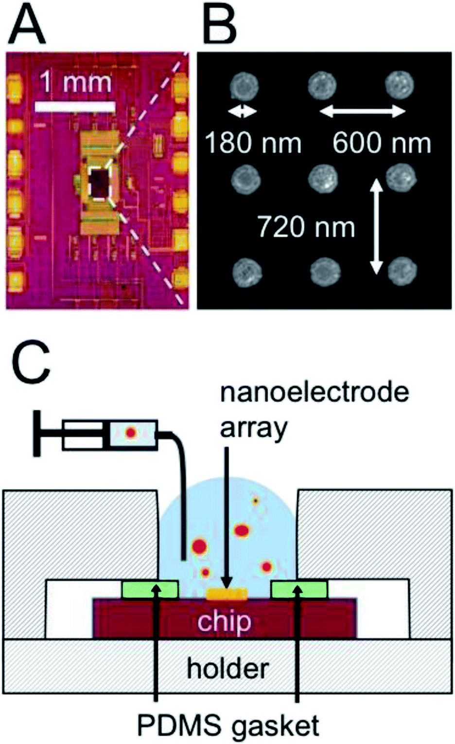 | ||
| Fig. 1 (A) Optical micrograph of the CMOS chip. (B) SEM image of a portion of the nanoelectrode array. (C) Cross-sectional schematic of the chip holder showing how the array of nanoelectrode is incubated in an emulsion solution. | ||
The AC response of each nanoelectrode was measured independently as follows. Each electrode was charged and discharged at a frequency f = 50 MHz, with a modulation voltage step of ΔEmod = 245 mV. The discharging current was integrated to obtain a charge and then digitalized with an on-chip analog-to-digital converter. The effective capacitance C was calculated by dividing the charge per cycle by the modulation voltage. The total impedance has two contributions in parallel: the stray capacitance from the metal interconnects in the CMOS chip and the impedance resulting from the nanoelectrode/solution interface. Although the stray capacitance is maintained at an extremely low level (typically 400 aF/nanoelectrode), we removed its contribution by subtracting a reference signal recorded in pure isopropanol. The relative capacitance scale used in the article is thus the effective capacitance measured with an emulsion, Cems, minus the capacitance measured in pure isopropanol, CIPA (ΔC = Cems − CIPA). This procedure allows not only to remove the stray capacitance but also to calibrate each individual electrode with a well-defined electrode/solution interface.
For representation, the capacitance value measured at each electrode was converted into a colored pixel and an image was reconstructed. A full frame (2 electrodes, area 228 μm × 154 μm (ref. 16)) was acquired every 0.2 s. Fig. 2A shows a typical capacitance image taken with a chip incubated for 1 min in an oDCB in water emulsion. An example of raw data (before CIPA subtraction) is also provided as Fig. S1 in the ESI.† This emulsion is used as a benchmark because of its relative stability (>15 min), its simple chemical composition (neither surfactant nor ions added) and its large range of droplet sizes. The diameter of the oDCB droplets, measured by optical microscopy (Fig. S2 in the ESI†), is between 1 and 40 μm. Here the polydispersity of the emulsion and the rapid sedimentation of the large droplets (density of oDCB 1.3 g mL−1)26 forbids characterization by DLS. The presence of oDCB droplets sedimented at the surface of the array is revealed by large capacitance variations, as seen in Fig. 2A. The blue background has an average capacitance of 120 ± 29 aF and corresponds to the water/electrode interface. The presence of oDCB droplets at the surface of the array is revealed by a decrease of the capacitance (green to red color Fig. 2A). Three distinct capacitance fingerprints are produced by the oDCB droplets. For each type of fingerprint, a typical capacitance image and the associated capacitance profile are provided in the top and bottom row of Fig. 2B, respectively. Cross-sectional schematics depicting the corresponding systems are shown in Fig. 2C.
 | ||
| Fig. 2 (A) Capacitance image obtained with a chip incubated for 1 min in an oDCB emulsion. Each pixel in this image represents one separately addressable electrode. The scale bar represents 20 μm. (B) Capacitance image (first row) and line profile (second row) of the individual oDCB droplets shown in the dashed white rectangles in (A). The capacitance image is plotted with a color scale that maximizes the contrast between oDCB and water. The line profiles have been normalized to the maximum capacitance in the whole array while the zero is set to the minimum value of the array. (C) Cross-sectional schematic depicting the systems producing the capacitance responses shown in (B). The red dashed line schematically represents the volume of solution probed by each nanoelectrode (yellow squares). The schematic is not to scale. | ||
The capacitance image, ΔC, and the corresponding line profile in Fig. 2B, column (i), shows a large spot with a sharp transition between water and oDCB as well as an homogeneous relative capacitance value (−10 ± 26 aF) inside the oDCB droplet. The typical diameter of such droplets varies between 3 and 20 μm. This fingerprint corresponds to the situation depicted in Fig. 2C column (i), with a droplet wetting the array. In this case the volume of solution probed by the nanoelectrodes (volume represented by the dashed red hemispheres in Fig. 2C) contains either pure oDCB or water and hence a two-level capacitance response is observed.
On the other hand, droplets that are not wetting the array produce a bell-shaped capacitance fingerprint (Fig. 2B, column (ii)). This profile, observed in a previous study of rigid polystyrene spheres, is caused by the spherical shape of the droplet in suspension (scheme in Fig. 2C column (ii)). It can be intuitively understood by the increasing content of water in the probing volume of a nanoelectrode, when the electrode is further from the center of the droplet. The FWHM of these Gaussian-like profiles is typically 5–10 μm. The actual diameter of a suspended droplet can be estimated by 3D finite-element simulations. Further details about the ENBIOS simulations and the determination of the droplet diameter are provided in the ESI (Fig. S3 and S4†). The estimated radius of the fully resolved, non-wetting oDCB droplets (see below and the ESI†) is between 2 μm and 10 μm. Another important value is the capacitance at the center of the droplet, about 65 ± 37 aF. This value, intermediate between the capacitance of pure water (120 aF) and pure oDCB (−10 aF), confirms that the droplet remains suspended and that a small amount of water lies between the nanoelectrode array and the bottom of the suspended droplet.
Finally, individual pixels (or less than 3 adjacent pixels) display capacitance changes ranging from −35 to 90 aF, as shown in Fig. 2B column (iii). These spikes are attributed to droplets of oDCB smaller than the pitch of the array and hence not spatially resolved (schematic Fig. 2C). In this case the droplets are too small to contribute significantly to the signal at remote electrodes.
Mapping the local relative permittivity
The large contrast of capacitance between oDCB and water observed in Fig. 2A clearly indicates that the magnitude of the capacitance change strongly depends on the composition of the solution near each electrode. The influence of the permittivity on the capacitance response of our CMOS chip was investigated by preparing emulsions with different oils having a relative permittivity between 2.4 (toluene) and 34.8 (nitrobenzene). A list of the different oils and their permittivity is provided in Table 1. Fig. 3A shows the capacitance measured at the center of large oil droplets and plotted as a function of the relative permittivity of the oil. The error bars represent the standard deviation between three independent measurements on different chips. The measured signal increases monotonically with the permittivity of the solution. A perfectly linear relationship between measured capacitance and permittivity is not observed, however. This could be caused by nonlinearities in the chip’s readout circuitry5 that become particularly significant here because of the significant variations in current levels encountered for the different oils. Nonetheless, the experimental curve of Fig. 3A can be used to calibrate the response of the chips and hence determine the relative permittivity of individual droplets a few microns in diameter. Interestingly, the coefficient of variation between chips (standard deviation/average value) is ∼12%, indicating that a reliable estimate of the dielectric constant can be obtained.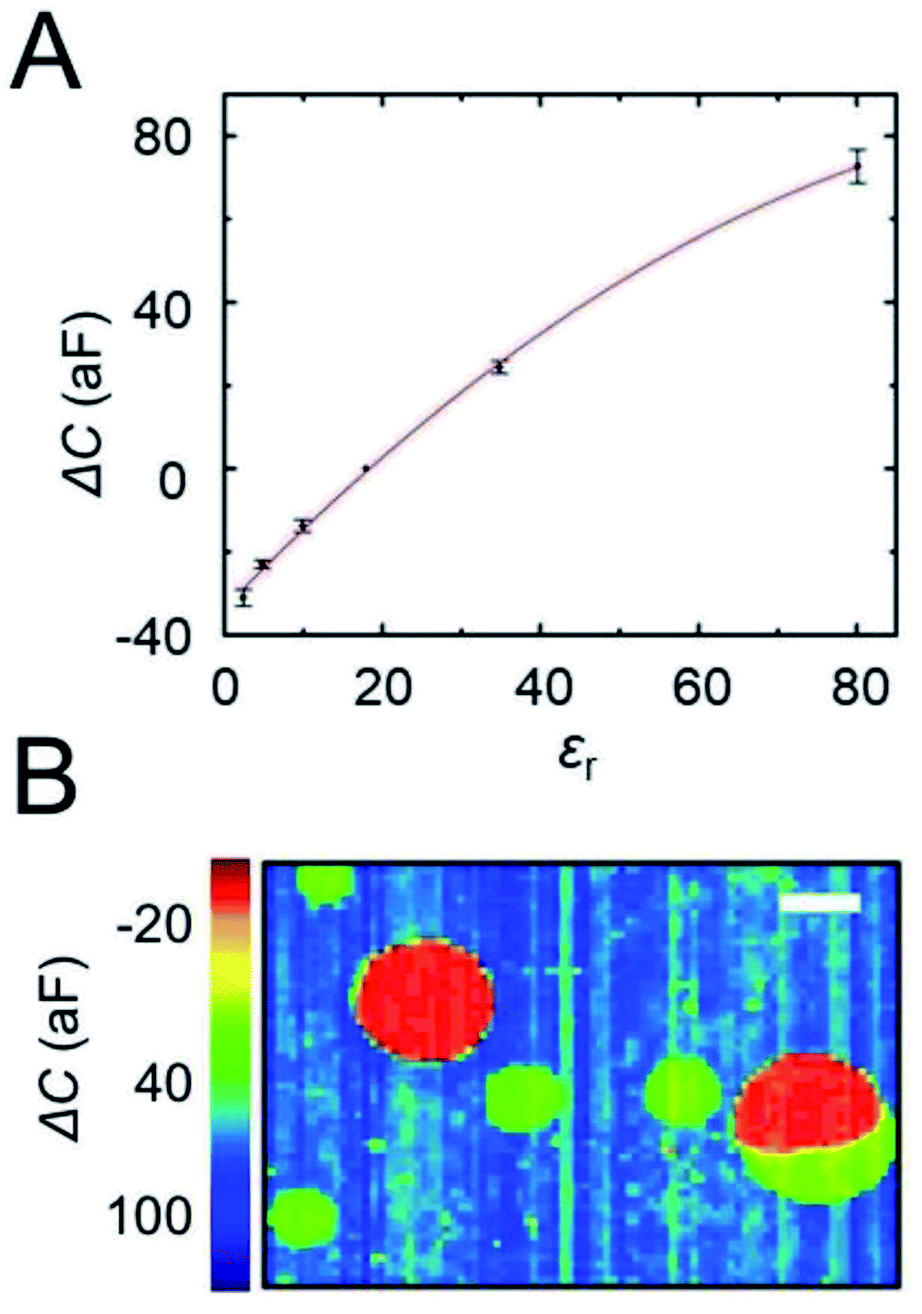 | ||
| Fig. 3 (A) Capacitance as a function of the relative dielectric constant of the medium. The red line is a guide to the eye. (B) Capacitance image of a chip incubated successively in a silicone oil and nitrobenzene emulsion. The scale bar represents 20 μm. | ||
| Solvent | ε r (at 25 °C) |
|---|---|
| Water | 80.1 |
| Nitrobenzene | 34.8 |
| Isopropanol | 17.9 |
| o-Dichlorobenzene | 9.9 |
| Chloroform | 4.8 |
| Toluene | 2.4 |
To illustrate this point, a chip was successively incubated with an emulsion of silicone oil (εr = 2.5) and an emulsion of nitrobenzene (εr = 34.8). The capacitance image of the chip, shown in Fig. 3B, clearly evidences two distinct populations of droplets corresponding to the two different solvents. Silicone oil droplets display an electrode capacitance of −21 ± 2 aF (red spots) while nitrobenzene droplets have a capacitance of 24 ± 3 aF relative to isopropanol. Based on the calibration curve (Fig. 3A) the corresponding value of εr for the silicone oil and nitrobenzene droplets are 6 ± 1 and 34 ± 3, respectively. The permittivity of nitrobenzene is in excellent agreement with the calibration value (εr = 34.8), while for the silicone oil a larger discrepancy is found (expected value εr = 2.5). The origin of this discrepancy in the mixture is not known at this time. Interestingly, the capacitance image of Fig. 2B also shows a large droplet composed of two phases with distinct values of permittivity (bottom right), one corresponding to silicone oil and the other to nitrobenzene. The boundary between these two phases can be clearly observed with an accuracy of about one micron, which corresponds to the pitch of the array.
Dynamics of individual droplets
We can take advantage of the temporal resolution of the capacitance imaging (0.2 s) to observe the electrostatic interactions between the surface of the chip and the oDCB droplets. This is illustrated in Fig. 4. Since the Si3N4 surface (∼95% of the total surface of the array) is negatively charged at pH 5.5–7 (isoelectric point 8)28 and the droplets do not instantly wet the surface, we conclude that the droplets are also negatively charged. This is in agreement with a value of zeta-potential of −53 mV measured on chlorobenzene in water droplets stabilized with a nonionic surfactant.29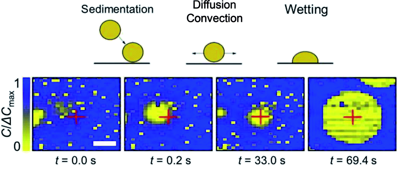 | ||
| Fig. 4 Illustration of the wetting dynamics. A droplet gradually approaches the surface of the array (first frame from the left), hovers and diffuses for some time above the surface (second and third frames) and eventually wets the array (right-most frame). The scale bar represents 3.3 μm. | ||
While the rapid dynamics of the wetting event itself do not allow its detailed analysis, it is possible to monitor the droplets’ movement before wetting. We used a particle tracking code (see Movie S2 in the ESI†) to automatically find the position of the droplets in each frame and reconstitute their trajectories over an entire movie. Fig. 4 shows typical frames in such a trajectory. The capacitance images display small droplets (less than 3 pixels) and larger ones comprised between 3 and 20 μm. The small droplets were not moving, while the movement of the larger droplets was sometimes caused by convection as evidenced by their quasi-linear trajectories and the linear dependence of the displacement with time. Convection was caused by the injection of the emulsion solution with a syringe and the subsequent elastic relaxation, inducing flow in the incubation chamber. Note also that some large droplets seemed not to move at all, or stopped moving after a period of time. These droplets could be either pinned by a local defect on the array or move extremely slowly solely by diffusion.
The capacitance movies also reveal interactions between droplets. Frames taken with an oDCB emulsion containing 1 mM of tetrabutylammonium toluene-4-sulfonate are shown in Fig. 5. These consecutive images show five oDCB droplets that merge together to form one large droplet. Interestingly, the first frame reveals that some oDCB droplets have high-capacitance inclusions inside the oDCB. The value of the capacitance, ca. 100 aF, corresponds to the permittivity of water. We thus conclude that some oDCB droplets contain smaller water droplets. Examination of Fig. 5B provides an important clue about the formation of these inclusions. The large droplet formed after merging contains four large inclusions and a smaller one near its center. We observed in several events like the one shown in Fig. 5, that the number of inclusions roughly matches the number of merging droplets. We thus conclude that these inclusions are formed by trapping some water between the droplets when they are merging. As shown in Fig. 5B the resulting droplet adopts an intermediate shape between a hemispherical shape that minimizes its surface area and the original position of the parent-droplets. The examination of several frames reveals that several seconds are necessary for such a large droplet to finally reach a quasi-spherical shape as shown in Fig. 5C. Such slow dynamics are typical for capillary relaxation.30
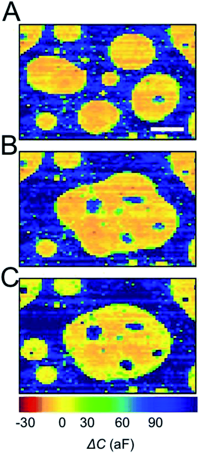 | ||
| Fig. 5 Capacitance images of oDCB droplets taken at 0 s (A), 0.2 s (B) and 5.1 s (C). The scale bar is the same for all images and represents 10 μm. The oDCB contains 1 mM of tetrabutylammonium toluene-4-sulfonate. | ||
Electrochemical contact angle measurements
An interesting consequence of being able to spatially resolve an individual droplet before and after wetting is the possibility of determining its contact angle θ. Some advantages of measuring contact angles at the μm scale, which is difficult using optical methods, include the possibility to reveal local (μm) inhomogeneities of the surface, simultaneous measurements on many droplets, and completely excluding gravitational effects (droplet deformation under its own weight). Spatially resolved electrochemical techniques such as SECM could also be employed in theory, to measure the contact angle. However, this would require the use of sub-micron sized tips (fragile and prone to fouling), an extremely skilled operator and several hours per droplet.To attempt to measure the contact angle, we followed the strategy presented in Fig. 6. The micrograph on the left shows a microdroplet of oDCB hovering at the surface of the array. At this stage the droplet did not wet the array and its shape was still spherical (sphere of radius r0) as depicted in the schematic on the left. Once the droplet wetted the array the situation depicted on the right was obtained. The droplet still tends to keep a spherical curvature to minimize its surface but the radius rwet is increased while its height h is reduced so that the total volume of the droplet is kept constant. The relation between θ, h and, rwet is given by (ESI†)
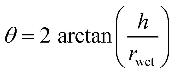 | (1) |
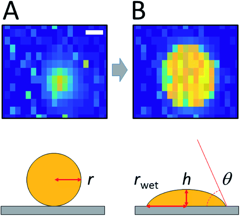 | ||
| Fig. 6 Capacitance image of an oDCB droplet before (A) and after (B) wetting the array. The schematics show the geometrical parameters that are obtained from the analysis of the CCD view. Scale bar represents 2.4 μm. | ||
The value of rwet can be directly measured from capacitance images. The radius of the droplet before spreading, r0, is deduced from numerical simulations of the capacitance image (ESI†). The value of h can then be calculated from r0 and rwet using eqn (5) in the ESI.†
This procedure is illustrated for several droplets in Table 2. Unfortunately, a significant systematic uncertainty is introduced in practice by the determination of the radius before wetting, r0. Two independent numerical approaches were employed based on either the second moment of the capacitive signal or the projected area of the particle in the image (ESI†). Table 2 indicates that the first method systematically yields droplet radii that are smaller than those of the second method. The origin of this discrepancy is not known at this point. It is possible that some physical properties of the system are not captured by the simulations. For example Maxwell–Wagner–Sillars polarization, which enhances the dielectric response of multiphasic systems at 50 MHz, could play a role.31
| Second moment method | Projected area method | ||||||
|---|---|---|---|---|---|---|---|
| # | r wet (μm) | r col (μm) | h (μm) | θ | r col (μm) | h (μm) | θ |
| 1 | 2.1 | 3.6 | 6.6 | 145 | 2.2 | 3.4 | 117 |
| 2 | 2.4 | 4.2 | 7.7 | 145 | 3.1 | 5.3 | 131 |
| 3 | 3.0 | 4.8 | 8.7 | 142 | 3.8 | 6.4 | 130 |
| 4 | 4.0 | 6.9 | 12.6 | 145 | 4.8 | 8.0 | 127 |
| 5 | 5.8 | 7.7 | 13.2 | 133 | 5.7 | 8.5 | 112 |
| 6 | 5.9 | 8.1 | 14.1 | 134 | 5.9 | 8.9 | 113 |
For comparison we also measured the contact angle of large oDCB droplets with a goniometer (Fig. S6†). The average contact angle measured on three different chips and droplets (three per chip) is 115 ± 1°. The contact angle measured with the chip on 6 droplets is estimated at 122 ± 9° using the projected area method (Table 2). The results on large droplets (1 μL) thus appear compatible with those on microscopic droplets (<pL).
Conclusions and outlook
Using oil micro-emulsions as prototypical systems, we have demonstrated several capabilities of the CMOS nanocapacitor array platform. These include the ability to image droplets of a few micrometers in size; detect individual sub-micrometer-sized droplets; obtain information on the composition of individual micro-droplets based on their physical parameters (in this case the dielectric constant); and observe the transport and wetting dynamics of droplets. By combining geometric information from before and after wetting, it is also, in principle, possible to infer the wetting angle of individual microdroplets, although additional work is needed to turn this approach into a quantitative assay. All of these observations are made possible by a combination of several strengths of nanocapacitor arrays, in particular the ability to reproducibly fabricate large arrays of nanoelectrodes, a high degree of integration that allows independently addressing these electrodes, and high-frequency operation. If mass-produced, these can serve as low-cost consumables for the characterization of a variety of hard-, soft- and biological-matter systems.Conflicts of interest
F. P. W. declares the following financial interest: he is the (co-)inventor of multiple patents on which the CMOS nanocapacitor platform is based and is employed by NXP, where it was developed.Acknowledgements
The authors thank H. A. Verhoeven for providing the holder and PDMS gaskets, M. Cirelli for the contact angle measurements and M. A. Smithers for the SEM measurements. We further gratefully acknowledge financial support from the European Research Council (ERC) under project number 278801.References
- G. S. Kulkarni, W. Zang and Z. Zhong, Acc. Chem. Res., 2016, 49, 2578–2586 CrossRef CAS PubMed.
- F. Widdershoven, D. Van Steenwinckel, J. Uberfeld, T. Merelle, H. Suy, F. Jedema, R. Hoofman, C. Tak, A. Sedzin, B. Cobelens, E. Sterckx, R. van der Werf, K. Verheyden, M. Kengen, F. Swartjes, F. Frederix and Ieee, in 2010 International Electron Devices Meeting – Technical Digest, 2010 Search PubMed.
- C. Laborde, F. Pittino, H. A. Verhoeven, S. G. Lemay, L. Selmi, M. A. Jongsma and F. P. Widdershoven, Nat. Nanotechnol., 2015, 10, 791–795 CrossRef CAS PubMed.
- S. G. Lemay, C. Laborde, C. Renault, A. Cossettini, L. Selmi and F. P. Widdershoven, Acc. Chem. Res., 2016, 49, 2355–2362 CrossRef CAS.
- F. Widdershoven, A. Cossettini, C. Laborde, A. Bandiziol, P. P. v. Swinderen, S. G. Lemay and L. Selmi, IEEE Trans. Biomed. Circuits Syst., 2018, 12, 1369–1382 Search PubMed.
- A. Cossettini, C. Laborde, D. Brandalise, F. Widdershoven, S. G. Lemay and L. Selmi, IEEE Sens. J., 2021, 21, 4696–4704 CAS.
- A. Cossettini, D. Brandalise, P. Palestri, A. Bertacchini, M. Ramponi, F. Widdershoven, L. Benini and L. Selmi, in 2020 Ieee Sensors, 2020, pp. 1–4 CAS.
- R. S. H. Lam and M. T. Nickerson, Food Chem., 2013, 141, 975–984 CrossRef CAS.
- J. Knowlton and S. Pearce, in Handbook of Cosmetic Science & Technology, Elsevier, 1993, pp. 95–118, DOI:10.1016/B978-1-85617-197-7.50013-7.
- C. W. Pouton, Adv. Drug Delivery Rev., 1997, 25, 47–58 CrossRef CAS.
- P. K. Kilpatrick, Energy Fuels, 2012, 26, 4017–4026 CrossRef.
- Y. Ouyang, R. S. Mansell and R. D. Rhue, Crit. Rev. Environ. Sci. Technol., 1995, 25, 269–290 CrossRef CAS.
- A. Imhof and D. J. Pine, Nature, 1997, 389, 948–951 CrossRef CAS.
- D. J. McClements, Food emulsions: principles, practices, and techniques, CRC Press, 2015 Search PubMed.
- J. E. Dick, C. Renault, B.-K. Kim and A. J. Bard, Angew. Chem., Int. Ed., 2014, 53, 11859–11862 CrossRef CAS PubMed.
- B.-K. Kim, A. Boika, J. Kim, J. E. Dick and A. J. Bard, J. Am. Chem. Soc., 2014, 136, 4849–4852 CrossRef CAS.
- B.-K. Kim, J. Kim and A. J. Bard, J. Am. Chem. Soc., 2015, 137, 2343–2349 CrossRef CAS.
- Y. Li, H. Deng, J. E. Dick and A. J. Bard, Anal. Chem., 2015, 87, 11013–11021 CrossRef CAS PubMed.
- T. Kakiuchi, M. Iida, S.-i. Imabayashi and K. Niki, Langmuir, 2000, 16, 5397–5401 CrossRef CAS.
- B. A. Ivarsson, P.-O. Hegg, K. I. Lundström and U. Jönsson, Colloids Surf., 1985, 13, 169–192 CrossRef CAS.
- P. Patil, M. Gorek, M. Folberth, A. Hartmann, S. Forgang, C. Fulda and K. Reinicke, SPE Drill. Completion, 2010, 25, 380–390 CAS.
- W. Q. Yang, A. L. Stott, M. S. Beck and C. G. Xie, Rev. Sci. Instrum., 1995, 66, 4326–4332 CrossRef CAS.
- F. Pittino and L. Selmi, Comput. Methods Appl. Mech. Eng., 2014, 278, 902–923 CrossRef.
- P. Scarbolo, F. Pittino, M. Dalla Longa, A. Cossettini and L. Selmi, ENBIOS-1D Lab, DOI:10.4231/D3Z02Z963.
- A. Hoxha, P. Scarbolo, A. Cossettini and L. Selmi, ENBIOS-2D Lab, DOI:10.4231/D3V11VM7D.
- W. M. Haynes, CRC handbook of chemistry and physics, CRC Press, 2014 Search PubMed.
- Engineering_ToolBox, Dielectric constants of liquids, https://www.engineeringtoolbox.com/liquid-dielectric-constants-d_1263.html Search PubMed.
- P. Greil, R. Nitzsche, H. Friedrich and W. Hermel, J. Eur. Ceram. Soc., 1991, 7, 353–359 CrossRef CAS.
- P. H. Elworthy, A. T. Florence and J. A. Rogers, J. Colloid Interface Sci., 1971, 35, 23–33 CrossRef.
- V. V. Khatavkar, P. D. Anderson and H. E. H. Meijer, J. Fluid Mech., 2007, 572, 367–387 CrossRef CAS.
- C. Grosse and A. V. Delgado, Curr. Opin. Colloid Interface Sci., 2010, 15, 145–159 CrossRef CAS.
Footnote |
| † Electronic supplementary information (ESI) available. See DOI: 10.1039/D1FD00044F |
| This journal is © The Royal Society of Chemistry 2022 |