
MoS2-capped CuxS nanocrystals: a new heterostructured geometry of transition metal dichalcogenides for broadband optoelectronics†
Yuan
Li
 abc,
Akshay A.
Murthy
be,
Jennifer G.
DiStefano
b,
Hee Joon
Jung
bc,
Shiqiang
Hao
b,
Cesar J.
Villa
b,
Chris
Wolverton
b,
Xinqi
Chen
*cd and
Vinayak P.
Dravid
*bce
abc,
Akshay A.
Murthy
be,
Jennifer G.
DiStefano
b,
Hee Joon
Jung
bc,
Shiqiang
Hao
b,
Cesar J.
Villa
b,
Chris
Wolverton
b,
Xinqi
Chen
*cd and
Vinayak P.
Dravid
*bce
aSchool of Materials Science and Engineering, Center of Advanced Lubrication and Seal Materials, Northwestern Polytechnical University, Xi'an, Shaanxi, 10072, China
bDepartment of Materials Science and Engineering, Northwestern University, Evanston, Illinois 60208, USA
cNorthwestern University Atomic and Nanoscale Characterization Experimental (NUANCE) Center, Northwestern University, Evanston, Illinois 60208, USA. E-mail: x-chen@northwestern.edu
dDepartment of Mechanical Engineering, Northwestern University, Evanston, Illinois 60208, USA
eInternational Institute for Nanotechnology (IIN), Northwestern University, Evanston, Illinois 60208, USA. E-mail: v-dravid@northwestern.edu
First published on 3rd January 2019
Abstract
Heterostructuring of different transition metal dichalcogenides (TMDs) leads to interesting band alignment and performance improvement, and thus enables new routes for the development of materials for next-generation semiconductor electronics. Herein, we introduce a new strategy for the design and synthesis of functional TMD heterostructures. The representative product, molybdenum disulfide-capped copper sulfide (CuxS@MoS2, 1.8 < x < 2.0), is typically obtained by chemical vapor deposition of cap-like MoS2 layers on CuxS nanocrystals, yielding the formation of a sharp, clean heterojunction interface. The heterostructures exhibit strong light–matter interactions over a broadband range, with interesting band alignment for separating photocarriers and mediating charge transfer. A phototransistor made from CuxS@MoS2 heterostructures shows particularly high photoresponse for near infrared light, which is enabled by the heterojunction of MoS2 with a small band gap semiconductor as well as the plasmonic enhancement from the CuxS nanocrystals. Our study paves a way for the development of new TMD heterostructures towards achieving functional electronics and optoelectronics.
Conceptual insightsConventional TMD heterostructures, aligned in lateral or vertical geometries (e.g., MoS2/WS2, MoSe2/WSe2, WSe2/MoS2, etc.), exhibit new chemical, structural and electronic properties for various applications in transistors, diodes and photovoltaic/photodetection devices. However, the main protocols, mechanical transfer and chemical vapor deposition, for preparing such heterostructures, are limited by their inevitable interface contamination and lack of massive and constant yields. Beyond the scope of such traditional heterostructures, our study reports a critical scientific step forward for bringing the concept of a new heterostructural geometry (namely MoS2-capped CuxS nanocrystals) into the family of TMD heterostructures. Using a direct chemical vapor deposition approach, we are able to create an atomically clean interface between the CuxS core and MoS2 cap, which, as compared with conventional TMD heterostructures, effectively maximized the interfacial area and would be very facile to realize large-scale production. Our structural design and synthesis strategy of the MoS2-capped CuxS nanocrystals can be generalized to abundant TMD materials and thus allow for a wide range of explorations across diverse disciplines and the originality of the approach. |
1. Introduction
Semiconductor heterostructures are essential components in modern high-speed electronics and optoelectronic devices.1 With the need for continued device scaling to achieve faster and miniaturized electronic components, new semiconductor systems such as two-dimensional (2D) transition metal dichalcogenides (TMDs) have attracted wide attention due to their unique layer-dependent electronic and optical properties.2–4 When these TMD semiconductors are combined in tandem, exciting new chemical, structural and electronic properties for various applications, such as transistors, diodes and photovoltaic/photodetection devices, are observed.5–10 For instance, heterostructures of layered TMDs (e.g., MoS2/WS2,7 MoSe2/WSe2,8 WSe2/MoS2,9,10etc.) have been demonstrated to form p–n junctions, which serve as the basis for these optoelectronic devices. The main function of these heterostructures is the ability to mediate optical transitions and charge transfer across the junction of two materials,11–13 and thus, maintaining a large-area, clean, and high-quality interface is of great importance. Unfortunately, to date most reported 2D heterostructures have been fabricated through mechanical transfer methods or multi-step chemical vapor deposition. While the former are troublesome due to the interfacial contamination commonly introduced via the polymer-based transfer process, the latter is problematic due to challenges related to the lack of spatial control over the synthesized products, more limited heterojunction interface, and lack of consistent yields.7Toward this end, exploring new geometries of TMD heterostructures beyond the existing library of 2D materials is of great interest for interface engineering and scalable production. Recently, surface decoration of TMD monolayers with nanocrystals14–16 or quantum dots17,18 of other chalcogenides has been studied as a typical approach to create heterojunctions. The resultant nanocomposites can effectively overcome the low optical cross-section of MoS2 and thus lead to enhanced absorption14 and improved photodetectivity.18 For instance, chalcocite copper sulfide (CuxS) nanocrystals are one of the most interesting materials due to their natural abundance, p-type semiconductor nature, and relatively small band gap leading to strong light absorption from the visible to near infrared region.19,20 When combined with MoS2, the resultant band alignment at the interfaces can potentially enable superior interfacial charge transfer.21,22 However, the reported preparation of the TMD heterostructures mostly relies on mechanical transfer14,15 or solution-based chemical synthesis16,17 and thus has been difficult to realize an uncontaminated and atomically-contacted sharp interface.
Herein, we introduce a new geometry design for the family of TMD heterostructures by encapsulating CuxS (1.8 < x < 2) nanocrystals with cap-like MoS2 layered structures, namely CuxS@MoS2 heterostructures. An atomically clean interface between the CuxS core and MoS2 cap is created via direct chemical vapor deposition, which effectively maximizes the interfacial area and thus facilitates photoemission and charge transfer between the two materials. Using discrete dipole approximation (DDA), we examined the optical properties of these heterostructures, and density functional theory (DFT) calculations were carried out to better understand the band alignment and charge transfer dynamics at the heterojunction interface. The viability of these heterostructures for photodetection applications was evaluated as well. The results indicate that our CuxS@MoS2 heterostructures exhibit highly improved light–matter interactions over a broad wavelength range compared to bare MoS2, and thus lead to a strong photoresponse from violet to near-infrared light.
2. Results and discussion
The synthesis of CuxS@MoS2 heterostructures is illustrated in Fig. 1a. Briefly, a 4 nm Cu film was first deposited on a Si/SiO2 substrate by thermal evaporation and then annealed at 600 °C in a N2 environment (step 1). The samples were then sulfurized at 600 °C (step 2) for 30 min. The encapsulation of MoS2 caps was finally accomplished via a chemical vapor deposition process utilizing MoO3 and S powders as precursors (step 3). The resultant product, CuxS@MoS2 heterostructures, is schematically illustrated in Fig. 1b. An optical image of the resultant sample surface is shown in Fig. 1c. The Cu film within the dotted lines was removed by scratching prior to MoS2 deposition. Thus, in this region, which exhibits a lighter optical contrast, we observed the growth of MoS2 monolayers with no CuxS. The flakes outside the dotted region exhibit a relatively darker color due to the formation of CuxS@MoS2 heterostructures, as indicated by the SEM images in Fig. 1d and e. One can also observe that the CuxS@MoS2 nanocrystals are distributed uniformly throughout the substrate. It is worth noting that the size and distribution of the nanocrystals can be effectively modulated by varying the thickness of the preliminary Cu film and the ramp rate of the subsequent annealing process, similar to that we have otherwise demonstrated previously.23 XRD patterns obtained over the entire substrate (Fig. S1, ESI†) indicate that the CuxS nanocrystals have a chalcocite structure with x varying from 1.8 to 2.0.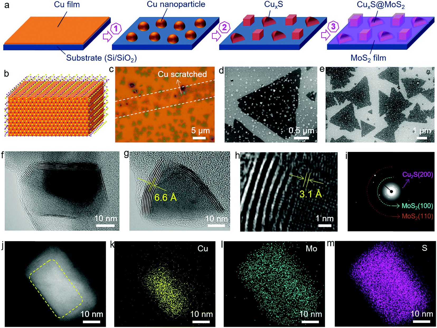 | ||
| Fig. 1 Synthesis of CuxS@MoS2 heterostructures. (a) Schematic illustrating the synthesis steps, including (1) annealing, (2) sulfurization, and (3) CVD. (b) Schematic of a single CuxS@MoS2 heterostructure, illustrating the cap-like MoS2 layers encapsulating a CuxS nanocrystal. (c) Optical view and (d and e) SEM images of the product after CVD. The substrate was left unexposed to the copper film in the dotted line region in (c). (f and g) TEM images of individual CuxS@MoS2 heterostructures. (h) High-resolution TEM image indicating the atomic contact at the CuxS–MoS2 interface and (i) the resultant diffraction pattern. (j) STEM image of a single heterostructure and (k–m) the corresponding EDS maps. | ||
The TEM images in Fig. 1f and g confirm that the MoS2 layers, with a layer-to-layer spacing of 6.6 Å and thickness of ∼3–5 nm, cap the faceted CuxS nanocrystals. The high-resolution image (Fig. 1h) further indicates the direct atomic connection of CuxS and MoS2 at the interface. CuxS exhibits a lattice spacing of 3.1 Å, corresponding to the (200) plane, which is also found to be the dominant facet of CuxS from the diffraction pattern (Fig. 1i). EDS maps obtained for a typical CuxS@MoS2 heterostructure (Fig. 1j) demonstrate the elemental composition of Cu, Mo and S (Fig. 1k–m). The distribution of Cu is mostly concentrated inside the heterostructure as outlined in Fig. 1j, indicating effective MoS2 encapsulation of the CuxS nanocrystals.
XPS spectra are further displayed in Fig. 2a–c. The spectra for the CuxS@MoS2 heterostructures are compared to a control sample prepared by transferring a pre-grown MoS2 monolayer onto CuxS nanocrystals (represented as CuxS/MoS2 hereafter). Details about the MoS2 transfer can be found in Fig. S2 (ESI†). The Mo and S spectra are generally consistent for both samples. The Mo 3d peaks at 233.11 eV and 229.92 eV correspond to the 3d5/2 and 3d3/2 doublets (Fig. 2a), while the S 2p peak can be deconvoluted into two peaks at 163.91 eV and 162.73 eV (Fig. 2b), which can be assigned to the 2p1/2 and 2p3/2 orbitals, respectively.24,25 The peaks for metallic Mo or MoOx are insignificant, suggesting high quality MoS2 layers on both products. The CuxS@MoS2 heterostructures present Cu 2p peaks at 952.32 eV (2p1/2) and 932.45 eV (2p3/2), which are consistent with the peak location of copper sulfides.26 However, the intensities of the Cu peaks are weaker compared with the Mo and S peaks, due to the encapsulation of the MoS2 layers. It is worth noting that peaks representing CuSO4 are also observed on the transferred samples, probably due to the inevitable surface oxidation of CuxS in air, which indicates that MoS2 encapsulation leads to improved air stability of the nanocrystals and serves as an additional highlight of this geometry.
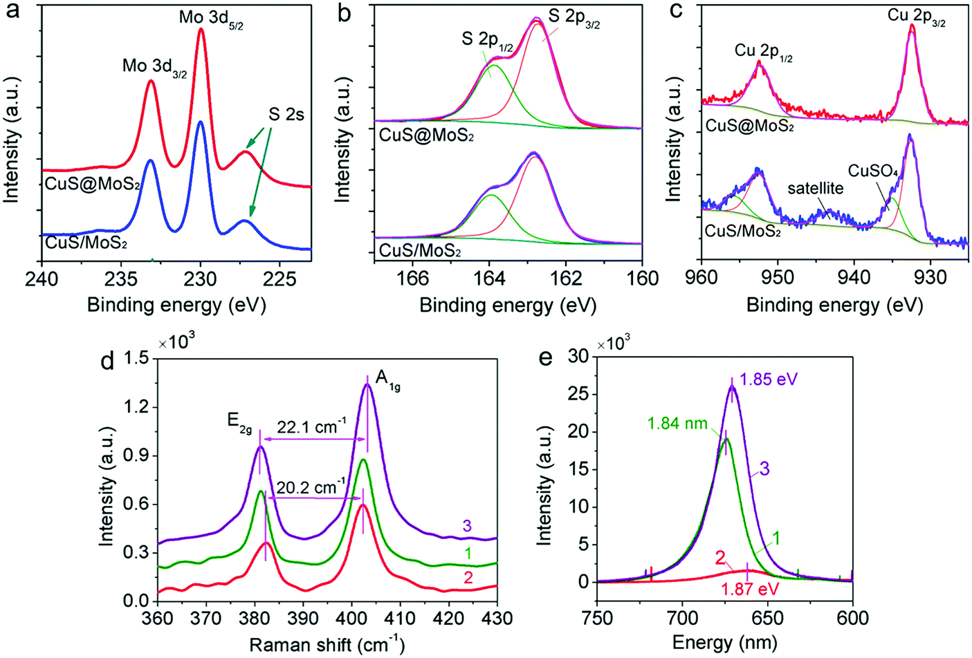 | ||
| Fig. 2 Spectroscopic characterization. (a–c) XPS spectra of (a) Mo 3d, (b) S 2p and (c) Cu 2p for the CuxS@MoS2 heterostructures and conventional MoS2 monolayer transferred onto CuxS nanocrystals. (d) Raman and (e) photoluminescence spectra of (1) monolayer MoS2 inside the dotted lines in Fig. 1c, (2) conventional MoS2 monolayer transferred onto CuxS nanocrystals and (3) CuxS@MoS2 heterostructures. | ||
Raman spectroscopy is used to assess the crystallinity and layer thickness of the MoS2 layers through the two characteristic MoS2 vibrational modes, E12g and A1g.25,27 The E12g mode is attributed to the in-plane vibration of Mo and S atoms, while the A1g mode is related to the out-of-plane vibration of S atoms.27Fig. 2d shows the Raman spectra of monolayer MoS2 (spectrum 1, obtained inside the dotted lines in Fig. 1b), CuxS/MoS2 (spectrum 2) and CuxS@MoS2 (spectrum 3). The CuxS@MoS2 heterostructures exhibit two vibrational modes centered at 381.10 cm−1 and 403.23 cm−1 with a E12g-to-A1g frequency difference of ∼22.13 cm−1. This value is smaller than that of bulk MoS2, but larger than that of the pristine and transferred monolayer MoS2, probably due to the multilayer nature of the MoS2 caps.28 The corresponding photoluminescence spectra are also collected at ambient temperature with a small laser power of 1 μW to avoid heating the sample. As shown in Fig. 2e, the pristine MoS2 exhibits photoluminescence emission near ∼674 nm and another insignificant emission peak around ∼623 nm. The former is attributed to the A exciton emission due to the interband transition at the Brillouin zone K point in MoS2, while the latter arises from the higher energy B exciton emission from another direct transition between the conduction band and a lower-lying valence band.29,30 The CuxS@MoS2 heterostructures exhibit equivalent photoluminescence emission peaks, with a slight blue-shift (670 nm) probably originating from the change in local strain because of the presence of CuxS cores.31 It is worth noting that a remarkable quenching effect and more significant blue-shift (to 663 nm) of the photoluminescence were observed for the transferred MoS2 sample, probably due to the inevitable contamination and released local strain from the original SiO2 substrate after the transfer process.32 This again proves the necessity of building a clean interface as demonstrated in our heterostructures.
The optical properties of the CuxS@MoS2 heterostructures are further understood using the discrete dipole approximation (DDA) method. The simulation was carried out for a 50 × 25 × 25 nm3 rectangular CuxS target and the same CuxS capped with 6-layer MoS2 as shown in Fig. 3a and b, respectively. The details regarding the DDA method can be found in the Experimental section (ESI†).33,34 The simulated absorption spectra are shown in Fig. 3c. The CuxS nanocrystal shows high absorption in the visible region (400 nm to 600 nm) as well as in the near infrared region (700 nm to 1000 nm), which is consistent with a previous experimental report.35 The CuxS@MoS2 heterostructure exhibits overall increased absorption in the visible region, with the emergence of two peaks at 673.1 nm and at 628.0 nm due to the presence of A and B exciton absorption pathways indicated in Fig. 3e.
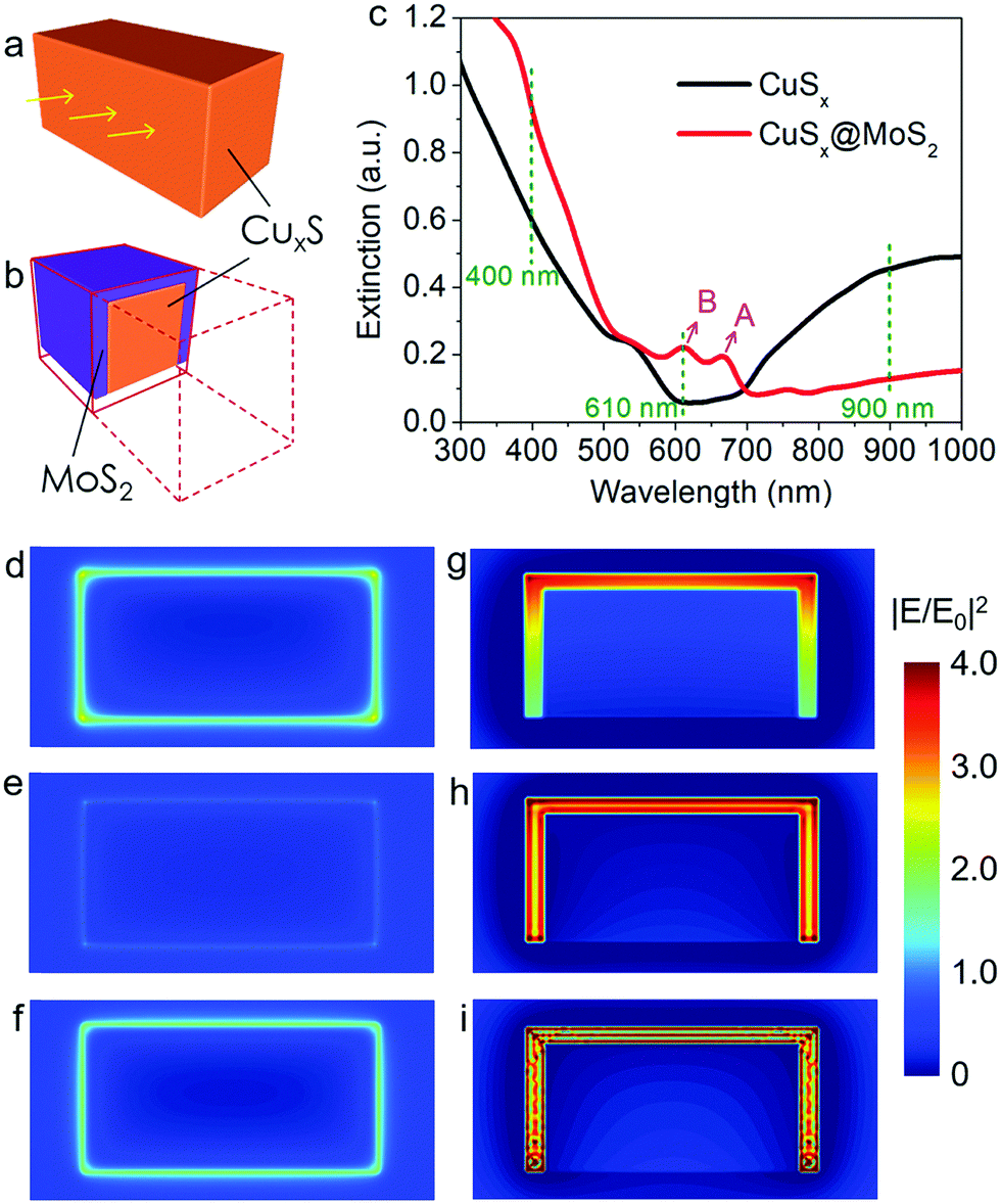 | ||
| Fig. 3 Simulation of light–matter interactions. (a and b) 3D models for the CuxS (a) and CuxS@MoS2 (b) targets used for DDA modeling. The arrows indicate the direction of incident light applied for all simulated targets unless otherwise noted. (c) Calculated extinction (absorption + scattering) efficiency as a function of incident wavelength. The A and B labels correspond to the A and B excitons observed in the photoluminescence spectra (Fig. 2e). (d–i) Calculated electric field distributions on CuxS (d–f) and CuxS@MoS2 (g–i) nanocrystals under various incident wavelengths: (d and g) 400 nm, (e and h) 610 nm, and (f and i) 900 nm. | ||
The DDA calculations also model the interaction of the refractive index with the geometry and incident light to evaluate the electric field distribution,33 which is an indicator of the magnitude of the light–matter interaction present. Fig. 3d–i display the front view (arrow direction in Fig. 3a) of the obtained electric field maps of both targets at different incident wavelengths (400 nm, 610 nm and 900 nm). The electric field strength (|E/E0|2) can be correlated with the absorption efficiency at various locations of the sample in Fig. 3c. Overall, one can observe that the CuxS nanocrystal shows a weak electric field response (Fig. 3d–f), while the electric field distribution of the CuxS@MoS2 heterostructure is confined to the MoS2 cap, with significantly enhanced strength (Fig. 3g–i), suggesting the significant improvement of the light–matter interactions due to the formation of a heterojunction. This aspect is particularly clear under an incident radiation of 900 nm, where even though coupling of light with the localized surface plasmon resonance (LSPR) of CuxS leads to an enhanced electric field in the bare nanocrystal.36,37 By contrast, the CuxS@MoS2 heterostructure exhibits a stronger response, due to the possible plasmonic coupling enabled by the clean CuxS–MoS2 interface.31 These simulations suggest that our CuxS@MoS2 heterostructure is a promising optoelectronic material particularly for applications where a near infrared source is required.
The DDA results theoretically suggest interesting light–matter interactions in our CuxS@MoS2 heterostructures, allowing us to further explore their potential application in broadband optoelectronics. A field-effect phototransistor made from the CuxS@MoS2 heterostructures was constructed with the schematic provided in Fig. 4a. In this device geometry, CuxS@MoS2 heterostructures act as the light sensitizers, while the underlying MoS2 monolayers act as the channel material (Fig. 4b). A similar transistor made from the transferred CuxS/MoS2 is also studied for comparison. All measurements were carried out at room temperature. As shown in Fig. 4c, the transferred CuxS/MoS2 device exhibits a typical n-type channel behavior, which is consistent with the n-type nature of monolayer MoS2.30 The CuxS@MoS2 device also shows an n-type electronic behavior; however, a gate-dependent drain current was only observed for small positive gate voltages before immediately saturating. This is possibly due to the Fermi level of MoS2 being aligned with that of p-type CuxS after the formation of the heterojunction. A further increase of the gate voltage in the positive direction can lead to misalignment in these bands, which would induce a decrease in the current.38 From the transfer curves, we obtain a carrier mobility of 1.76 × 10⁻⁴ cm2 V−1 s−1 for the CuxS@MoS2 device and 0.11 × 10⁻⁴ cm2 V−1 s−1 for the CuxS/MoS2 device. It is also worth noting that both devices show a relatively weak gate dependence with ON/OFF ratios of 1.2–1.5,39 which is probably due to the electric field screening provided by the underlying CuxS nanocrystals. The dependence of transfer curves on the illumination power for the CuxS/MoS2 and CuxS@MoS2 transistors is demonstrated in Fig. 4d and e, respectively. Both devices show a photocurrent generation ability over the entire gate voltage range, which is also consistent with the results previously reported for monolayer MoS2 transistors.40 However, the photoresponse of the CuxS@MoS2 device is more significant, with a negligible gate dependence, and exhibits a linear relationship with the increase of illumination power, which is usually more desirable for practical optoelectronics.
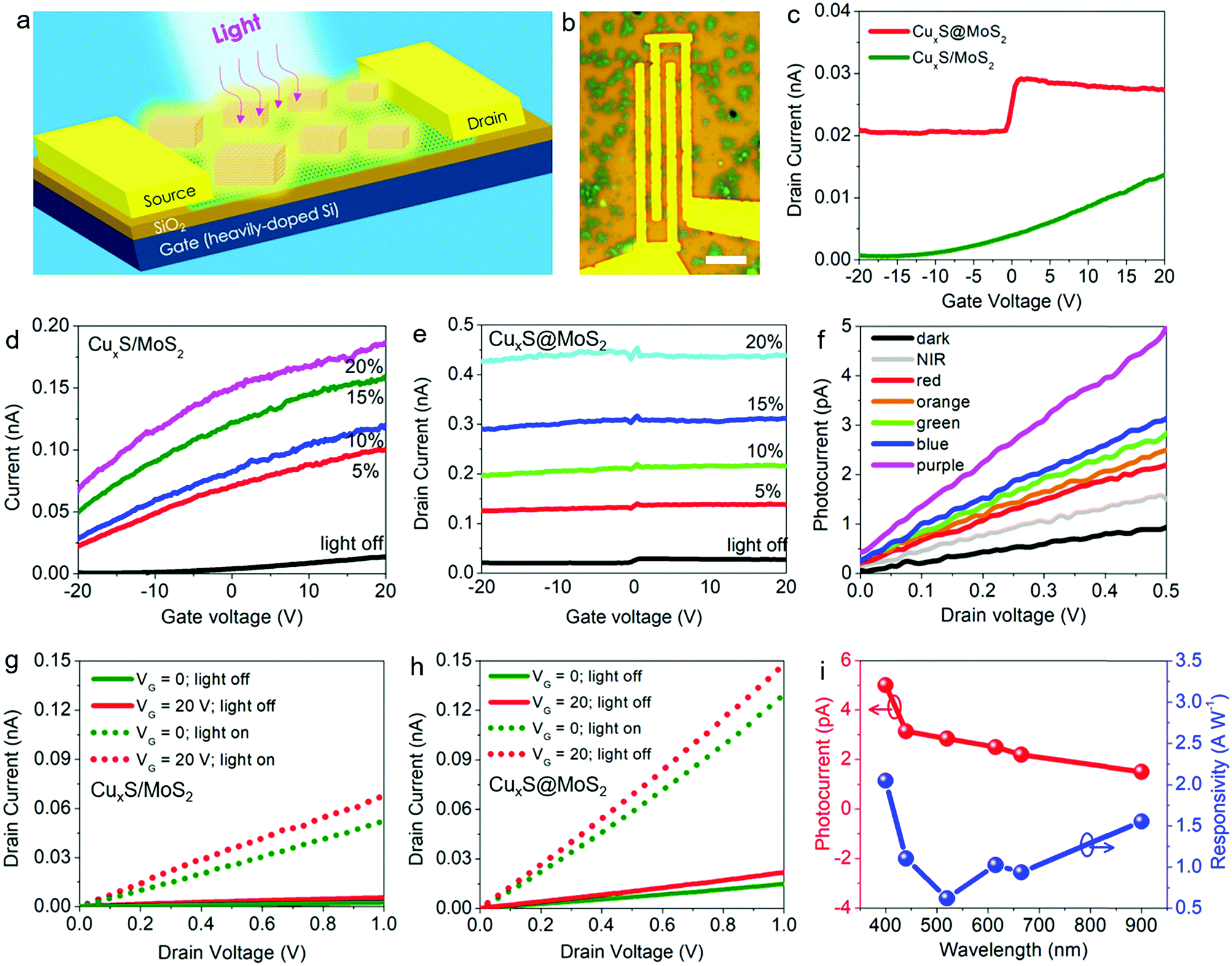 | ||
| Fig. 4 Optoelectronic device application. (a) Device design and (b) optical view of the phototransistor. Scale bar in (b): 5 μm. (c) Transfer characteristics of the CuxS/MoS2 and CuxS@MoS2 devices. (d and e) Transfer curves of CuxS/MoS2 (d) and CuxS@MoS2 (e) transistors under illumination with varying power. (f and g) Output curves of CuxS/MoS2 (f) and CuxS@MoS2 (g) transistors with and without illumination. (h) Output curve of the CuxS@MoS2 device with illuminations of different wavelengths. (i) Photocurrent and photoresponsivity of the CuxS@MoS2 device as a function of illumination wavelength. | ||
The output curves in the dark and light states for both devices are further shown in Fig. 4f and g. It is worth mentioning that the linear relationship between the drain current and drain voltage indicates good ohmic contact of the channel materials and contact electrodes. One can again observe that the CuxS@MoS2 device exhibits a more substantial photoresponse compared to the CuxS/MoS2 device. The output curves of the CuxS@MoS2 device at various illumination wavelengths are shown in Fig. 4h. The device shows remarkable response for wavelengths ranging from the violet to near infrared region due to the presence of small-band gap CuxS, which is one of the key advantages of the heterostructure compared to MoS2 devices. The corresponding photocurrent and the calculated photoresponsivity are further displayed in Fig. 4i. The trend of photoresponsivity variation according to the incident wavelength is consistent with the absorption curve of CuxS@MoS2 in Fig. 3c. It is worth noting that the photoresponsivity under near infrared incident radiation is significantly pronounced compared to the absorption spectra (consistent with the near field distribution in Fig. 3i). This should be enabled by (1) the band bending and electric fields present at the heterojunction interface between MoS2 and a small-band gap material and (2) possibly the strong light–matter interaction due to the LSPR effect as theoretically predicted in Fig. 3i and experimentally demonstrated in our previous report,41 further suggesting the potential of our TMD heterostructures in broadband optoelectronics.
Finally, we performed density functional theory (DFT) calculations to understand and corroborate our experimental findings and conclusions regarding the optoelectronic properties of this heterostructure. Fig. 5a shows high symmetry points in the Brillouin zone of CuxS (inset atomic structure) used for the calculation. The obtained electronic band structures for Cu2S and Cu1.8S are shown in Fig. 5b and c, respectively. We find that the ideal chalcocite Cu2S has an indirect band gap of 0.56 eV; however, the band structure can be effectively modulated by introducing Cu vacancies in the system. For instance, the chalcocite Cu1.8S is found to exhibit a direct band gap of 0.55 eV (Fig. 5c). This suggests that the incorporation of CuxS can not only supplement the low IR absorption for MoS2 (Fig. 3c), but also significantly improve the photoelectronic effect since the photon-related excitation and emission in the slightly deficient CuxS are significantly improved.
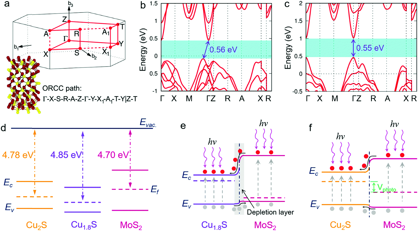 | ||
| Fig. 5 Electronic structure calculations. (a) High symmetry points in the Brillouin zone of CuxS. The inset shows the corresponding atomic structure. (b and c) Band structures calculated for Cu2S (b) and Cu1.8S (c). (d) Calculated energy band diagram for Cu2S, Cu1.8S, and MoS2. (e and f) Schematics showing the possible formation of a type-II heterojunction between Cu1.8S and MoS2 (e) and a type-I heterojunction between Cu2S and MoS2 (f) under illumination. | ||
The DFT calculations also reveal the work function of the components, which allows us to predict the alignment of the band structure at the interface. Fig. 5d shows the band energy diagram of the Cu2S, Cu1.8S and MoS2 systems before heterojunction formation. Again, this directly indicates the modulation of the band structure of CuxS with slight variations in the stoichiometry (see more details in Fig. S3, ESI†), and accordingly we are able to predict possible charge transfer pathways following heterojunction formation. As shown in Fig. 5e and f, CuxS–MoS2 is expected to exhibit better photocarrier separation efficiency due to the formation of a type-II band alignment (Fig. 5e), as compared with the possible type-I heterojunction formed in the Cu2S–MoS2 system (Fig. 5f). Thus, combined with evidence from our optical results, we can surmise that the noteworthy optoelectronic performance of our CuxS@MoS2 phototransistor is probably attributed to a comprehensive contribution from (1) the improved interfacial charge transfer that originated from the clean, atomically-connected interface, (2) the formation of a type-II heterojunction structure between CuxS and MoS2, and (3) the potentially enhanced light–matter interactions due to the LSPR of CuxS.
3. Conclusions
In summary, we explored a new route for the geometry design and synthesis of TMD heterostructures beyond traditional lateral/vertical heterostructures. The heterojunction formation was accomplished via a single-step direct chemical vapor deposition of MoS2 on nanocrystals of another transition metal sulfide. The resultant product, e.g., CuxS@MoS2 heterostructures, has an appreciable atomically-sharp interface area and is found to exhibit strongly improved light–matter interactions over a broad wavelength range. The formation of this heterojunction also leads to useful band alignment and can potentially facilitate the charge separation and transfer in an optoelectronic process. The field-effect phototransistor based on the CuxS@MoS2 heterostructures represents interesting transfer characteristics, and importantly, a constant photoresponse is observed throughout the entire positive and negative gate voltage regions. The photocurrent generation was observed over a broadband range, particularly for the near infrared photodetection enabled by the band alignment at the heterojunction as well as the surface plasmon effect from CuxS. As such, this geometry potentially serves as a new scalable material system for future optoelectronic semiconductor devices.Conflicts of interest
There are no conflicts to declare.Acknowledgements
This material is based on the work supported by the National Science Foundation (NSF) under Grant No. DMR-1507810. This work made use of the EPIC, Keck-II, and SPID facilities of Northwestern University's NUANCE Center, which received support from the Soft and Hybrid Nanotechnology Experimental (SHyNE) Resource (NSF ECCS-1542205); the MRSEC program (NSF DMR-1720139) at the Materials Research Center; the International Institute for Nanotechnology (IIN); the Keck Foundation; and the State of Illinois, through the IIN. J. G. D. gratefully acknowledges support from the National Science Foundation Graduate Research Fellowship Program (NSF-GRFP). A. A. M. gratefully acknowledges support from the Ryan Fellowship and the International Institute for Nanotechnology at Northwestern University.References
- Q. H. Wang, K. Kalantar-Zadeh, A. Kis, J. N. Coleman and M. S. Strano, Electronics and Optoelectronics of Two-Dimensional Transition Metal Dichalcogenides, Nat. Nanotechnol., 2012, 7, 699 CrossRef CAS PubMed.
- M. Chhowalla, D. Jena and H. Zhang, Two-dimensional semiconductors for transistors, Nat. Rev. Mater., 2016, 1, 16052 CrossRef CAS.
- C. Tan, Z. Liu, W. Huang and H. Zhang, Non-volatile resistive memory devices based on solution-processed ultrathin two-dimensional nanomaterials, Chem. Soc. Rev., 2015, 44, 2615 RSC.
- H. Zhang, Ultrathin two-dimensional nanomaterials, ACS Nano, 2015, 9, 9451 CrossRef CAS PubMed.
- X. Zhang, Z. Lai, Q. Ma and H. Zhang, Novel structured transition metal dichalcogenide nanosheets, Chem. Soc. Rev., 2018, 47, 3301 RSC.
- C. Tan, X. Cao, X. Wu, Q. He, J. Yang, X. Zhang, J. Chen, W. Zhao, S. Han, G. H. Nam, M. Sindoro and H. Zhang, Recent advances in ultrathin two-dimensional nanomaterials, Chem. Rev., 2017, 117, 6225 CrossRef CAS PubMed.
- Y. Gong, J. Lin, X. Wang, G. Shi, S. Lei, Z. Lin and H. Terrones, Vertical and in-plane heterostructures from WS2/MoS2 monolayers, Nat. Mater., 2014, 13, 1135 CrossRef CAS PubMed.
- C. Huang, S. Wu, A. M. Sanchez, J. J. Peters, R. Beanland, J. S. Ross and X. Xu, Lateral heterojunctions within monolayer MoSe2–WSe2 semiconductors, Nat. Mater., 2014, 13, 1096 CrossRef CAS PubMed.
- M. Y. Li, Y. Shi, C. C. Cheng, L. S. Lu, Y. C. Lin, H. L. Tang and W. H. Chang, Epitaxial growth of a monolayer WSe2–MoS2 lateral pn junction with an atomically sharp interface, Science, 2015, 349, 524 CrossRef CAS PubMed.
- X. Duan, C. Wang, J. C. Shaw, R. Cheng, Y. Chen, H. Li and J. Jiang, Lateral epitaxial growth of two-dimensional layered semiconductor heterojunctions, Nat. Nanotechnol., 2014, 9, 1024 CrossRef CAS PubMed.
- F. Ceballos, M. Z. Bellus, H. Y. Chiu and H. Zhao, Ultrafast charge separation and indirect exciton formation in a MoS2–MoSe2 van der Waals heterostructure, ACS Nano, 2014, 8, 12717 CrossRef CAS PubMed.
- H. Chen, X. Wen, J. Zhang, T. Wu, Y. Gong, X. Zhang and W. Zhuang, Ultrafast formation of interlayer hot excitons in atomically thin MoS2/WS2 heterostructures, Nat. Commun., 2016, 7, 12512 CrossRef CAS PubMed.
- D. Kozawa, A. Carvalho, I. Verzhbitskiy, F. Giustiniano, Y. Miyauchi, S. Mouri and G. Eda, Evidence for fast interlayer energy transfer in MoSe2/WS2 heterostructures, Nano Lett., 2016, 16, 4087 CrossRef CAS PubMed.
- X. Sun, H. Deng, W. Zhu, Z. Yu, C. Wu and Y. Xie, Interface Engineering in Two-Dimensional Heterostructures: Towards an Advanced Catalyst for Ullmann Couplings, Angew. Chem., Int. Ed., 2016, 55, 1704 CrossRef CAS PubMed.
- Y. Wen, L. Yin, P. He, Z. Wang, X. Zhang, Q. Wang and F. Wang, Integrated high-performance infrared phototransistor arrays composed of nonlayered PbS–MoS2 heterostructures with edge contacts, Nano Lett., 2016, 16, 6437 CrossRef CAS PubMed.
- P. Sahatiya, A. Kadu, H. Gupta, P. Thanga Gomathi and S. Badhulika, Flexible disposable cellulose paper based MoS2–Cu2S hybrid for wireless environmental monitoring and multifunctional sensing of chemical stimuli, ACS Appl. Mater. Interfaces, 2018, 10, 9048 CrossRef CAS PubMed.
- J. Schornbaum, B. Winter, S. P. Schießl, F. Gannott, G. Katsukis, D. M. Guldi and J. Zaumseil, Epitaxial Growth of PbSe Quantum Dots on MoS2 Nanosheets and their Near-Infrared Photoresponse, Adv. Funct. Mater., 2014, 24, 5798 CrossRef CAS.
- D. Kufer, I. Nikitskiy, T. Lasanta, G. Navickaite, F. H. Koppens and G. Konstantatos, Hybrid 2D–0D MoS2–PbS quantum dot photodetectors, Adv. Mater., 2015, 27, 176 CrossRef CAS PubMed.
- A. B. Wong, S. Brittman, Y. Yu, N. P. Dasgupta and P. Yang, Core–shell CdS–Cu2S nanorod array solar cells, Nano Lett., 2015, 15, 4096 CrossRef CAS PubMed.
- A. B. Martinson, S. C. Riha, E. Thimsen, J. W. Elam and M. J. Pellin, Structural, optical, and electronic stability of copper sulfide thin films grown by atomic layer deposition, Energy Environ. Sci., 2013, 6, 1868 RSC.
- Y. Wang, H. Li, Y. Zhang, Y. Peng, P. Zhang and J. Zhao, Self-templating thermolysis synthesis of Cu2–xS@M (M = C, TiO2, MoS2) hollow spheres and their application in rechargeable lithium batteries, Nano Res., 2018, 11, 831 CrossRef CAS.
- C. Pan, S. Niu, Y. Ding, L. Dong, R. Yu, Y. Liu and Z. L. Wang, Enhanced Cu2S/CdS coaxial nanowire solar cells by piezo-phototronic effect, Nano Lett., 2012, 12, 3302 CrossRef CAS PubMed.
- Y. Li, K. Burnham, J. Dykes and N. Chopra, Self-patterning of graphene-encapsulated gold nanoparticles for surface-enhanced Raman spectroscopy, MRS Commun., 2018, 8, 79 CrossRef CAS.
- K. M. McCreary, A. T. Hanbicki, J. T. Robinson, E. Cobas, J. C. Culbertson, A. L. Friedman and B. T. Jonker, Adv. Funct. Mater., 2014, 24, 6449 CrossRef CAS.
- A. S. George, Z. Mutlu, R. Ionescu, R. J. Wu, J. S. Jeong, H. H. Bay and C. S. Ozkan, Adv. Funct. Mater., 2014, 24, 7461 CrossRef CAS.
- M. C. Biesinger, B. R. Hart, R. Polack, B. A. Kobe and R. S. C. Smart, Analysis of mineral surface chemistry in flotation separation using imaging XPS, Miner. Eng., 2007, 20, 152 CrossRef CAS.
- S. Wang, X. Wang and J. H. Warner, All Chemical Vapor Deposition Growth of MoS2: h-BN Vertical van der Waals Heterostructures, ACS Nano, 2015, 9, 5246 CrossRef CAS PubMed.
- H. Li, Q. Zhang, C. C. R. Yap, B. K. Tay, T. H. T. Edwin, A. Olivier and D. Baillargeat, From bulk to monolayer MoS2: evolution of Raman scattering, Adv. Funct. Mater., 2012, 22, 1385 CrossRef CAS.
- G. Eda, H. Yamaguchi, D. Voiry, T. Fujita, M. Chen and M. Chhowalla, Photoluminescence from chemically exfoliated MoS2, Nano Lett., 2011, 11, 5111 CrossRef CAS PubMed.
- W. Choi, M. Y. Cho, A. Konar, J. H. Lee, G. B. Cha, S. C. Hong and S. Kim, High-Detectivity Multilayer MoS2 Phototransistors with Spectral Response from Ultraviolet to Infrared, Adv. Mater., 2012, 24, 5832 CrossRef CAS PubMed.
- Y. Li, J. D. Cain, E. D. Hanson, A. A. Murthy, S. Hao, F. Shi, Q. Li, C. Wolverton, X. Chen and V. P. Dravid, Au@ MoS2 core–shell heterostructures with strong light–matter interactions, Nano Lett., 2016, 16, 7696 CrossRef CAS PubMed.
- W. H. Chae, J. D. Cain, E. D. Hanson, A. A. Murthy and V. P. Dravid, Substrate-induced strain and charge doping in CVD-grown monolayer MoS2, Appl. Phys. Lett., 2017, 111, 143106 CrossRef.
- B. T. Draine and P. J. Flatau, User guide for the discrete dipole approximation code DDSCAT 7.3, 2013, arXiv preprint arXiv, 1305.6497.
- Y. Li, W. Shi and N. Chopra, Functionalization of multilayer carbon shell-encapsulated gold nanoparticles for surface-enhanced Raman scattering sensing and DNA immobilization, Carbon, 2016, 100, 165 CrossRef CAS.
- A. C. Poulose, S. Veeranarayanan, M. S. Mohamed, Y. Nagaoka, R. R. Aburto, T. Mitcham and T. Maekawa, Multi-stimuli responsive Cu2S nanocrystals as trimodal imaging and synergistic chemo-photothermal therapy agents, Nanoscale, 2015, 7, 8378 RSC.
- J. M. Luther, P. K. Jain, T. Ewers and A. P. Alivisatos, Localized surface plasmon resonances arising from free carriers in doped quantum dots, Nat. Mater., 2011, 10, 361 CrossRef CAS PubMed.
- Y. Xie, A. Riedinger, M. Prato, A. Casu, A. Genovese, P. Guardia, S. Sottini, C. Sangregorio, K. Miszta and S. Ghosh, Copper Sulfide Nanocrystals with Tunable Composition by Reduction of Covellite Nanocrystals with Cu+ ions, J. Am. Chem. Soc., 2013, 135, 17630 CrossRef CAS PubMed.
- D. Jariwala, V. K. Sangwan, C. C. Wu, P. L. Prabhumirashi, M. L. Geier, T. J. Marks and M. C. Hersam, Gate-Tunable Carbon Nanotube–MoS2 Heterojunction pn Diode, Proc. Natl. Acad. Sci. U. S. A., 2013, 110, 18076 CrossRef CAS PubMed.
- Z. Yin, H. Li, H. Li, L. Jiang, Y. Shi, Y. Sun and H. Zhang, Single-layer MoS2 phototransistors, ACS Nano, 2011, 6, 74 CrossRef PubMed.
- O. Lopez-Sanchez, D. Lembke, M. Kayci, A. Radenovic and A. Kis, Ultrasensitive photodetectors based on monolayer MoS2, Nat. Nanotechnol., 2013, 8, 497 CrossRef CAS PubMed.
- Y. Li, J. G. DiStefano, A. A. Murthy, J. D. Cain, E. D. Hanson, Q. Li, F. C. Castro, X. Chen and V. P. Dravid, Superior Plasmonic Photodetectors Based on Au@ MoS2 Core–Shell Heterostructures, ACS Nano, 2017, 11, 10321 CrossRef CAS PubMed.
Footnote |
| † Electronic supplementary information (ESI) available: Experimental details; XRD characterization; and transfer of a CVD-grown MoS2 monolayer onto CuxS nanocrystals. See DOI: 10.1039/c8mh00809d |
| This journal is © The Royal Society of Chemistry 2019 |